
Photoexcited carrier dynamics in colloidal quantum dot solar cells: insights into individual quantum dots, quantum dot solid films and devices
Yaohong
Zhang
 a,
Guohua
Wu
*b,
Feng
Liu
a,
Chao
Ding
a,
Zhigang
Zou
*c and
Qing
Shen
*a
a,
Guohua
Wu
*b,
Feng
Liu
a,
Chao
Ding
a,
Zhigang
Zou
*c and
Qing
Shen
*a
aFaculty of Informatics and Engineering, The University of Electro-Communications, Tokyo 182-8585, Japan. E-mail: shen@pc.uec.ac.jp
bSchool of Materials Science and Engineering, Shaanxi Normal University, Xi'an 710119, China. E-mail: ghwu@snnu.edu.cn
cEcomaterials and Renewable Energy Research Center, Jiangsu Key Laboratory for Nano Technology, National Laboratory of Solid State Microstructures, Nanjing University, Nanjing 210093, China. E-mail: zgzou@nju.edu.cn
First published on 11th December 2019
Abstract
The certified power conversion efficiency (PCE) record of colloidal quantum dot solar cells (QDSCs) has considerably improved from below 4% to 16.6% in the last few years. However, the record PCE value of QDSCs is still substantially lower than the theoretical efficiency. So far, there have been several reviews on recent and significant achievements in QDSCs, but reviews on photoexcited carrier dynamics in QDSCs are scarce. The photovoltaic performances of QDSCs are still limited by the photovoltage, photocurrent and fill factor that are mainly determined by the photoexcited carrier dynamics, including carrier (or exciton) generation, carrier extraction or transfer, and the carrier recombination process, in the devices. In this review, the photoexcited carrier dynamics in the whole QDSCs, originating from individual quantum dots (QDs) to the entire device as well as the characterization methods used for analyzing the photoexcited carrier dynamics are summarized and discussed. The recent research including photoexcited multiple exciton generation (MEG), hot electron extraction, and carrier transfer between adjacent QDs, as well as carrier injection and recombination at each interface of QDSCs are discussed in detail herein. The influence of photoexcited carrier dynamics on the physiochemical properties of QDs and photovoltaic performances of QDSC devices is also discussed.
 Yaohong Zhang | Yaohong Zhang obtained his BSc from Soochow University in 2009. He received his MSc from Institute of Plasma Physics, Chinese Academy of Sciences (CAS) in 2012. Subsequently, he joined Fujian Institute of Research on the Structure of Matter, CAS as a research assistant with interest in photocatalysis for two years. In 2017, he received his PhD from the University of Electro-Communications (UEC) under the supervision of Prof. Qing Shen. Currently, he is working as a project researcher in UEC. His research is focused on optoelectronic nanomaterials and their application in photovoltaics and photocatalysis as well as their corresponding carrier dynamics study. |
 Guohua Wu | Guohua Wu received her BSc from Shandong Normal University in 2009. In 2014, she obtained her PhD in Materials Physics and Chemistry from the Hefei Institute of Physical Science, Chinese Academy of Sciences. Subsequently, she joined the research group of Prof. Joe Otsuki at Nihon University in Tokyo as a postdoctoral fellow from Oct. 2014 to Dec. 2017. She then moved to Shaanxi Normal University as an associate professor. Her research interests include the organic–inorganic optoelectronic functional materials, supramolecular chemistry and photovoltaic devices. |
 Feng Liu | Feng Liu obtained his PhD in Material Physics and Chemistry from University of Chinese Academy of Sciences in 2016. He subsequently joined Prof. Shen's group at University of Electro-Communications (UEC) as an UEC postdoctoral research fellow. In 2018, he was awarded the “FY2018 JSPS Postdoctoral Fellowship for Foreign Researchers” by the Japan Society for the Promotion of Sciences (JSPS). He is currently working as a JSPS postdoctoral researcher in Prof. Shen's group at UEC. His research focuses on perovskite nanomaterials and their applications in optoelectronic devices. |
 Chao Ding | Chao Ding received his BSc (2011) and MSc (2014) degrees in Materials Physics and Chemistry from Sichuan University, China and PhD (2018) degree in the Department of Engineering Science from The University of Electro-Communications, Japan. Currently, he is a postdoctoral research fellow in Prof. Qing Shen's Group. His research interests include development of emerging photovoltaic based materials (colloidal quantum dot and perovskite solar cells); ultrafast spectroscopy study of photophysics in colloidal nanocrystals; carrier dynamics in light harvesting, and emitting devices. |
 Zhigang Zou | Zhigang Zou is now the “Yangtze River Scholars” Distinguished Professor at Nanjing University, the academician of the Chinese Academy of Science, and the academician of the Third World Academy of Science. He has long-term devoted himself to the research field of new energy and nanomaterials, where he has made systematic and original contributions to the theory development, material preparation, and applications of energy and environmental materials, specifically the new-generation photocatalytic materials and solar cells. |
 Qing Shen | Qing Shen obtained her PhD from the University of Tokyo in 1995. Subsequently, she joined the University of Electro-Communications (UEC). Currently, she is a professor of UEC. Her main topics of research interest are nanomaterials and their applications in optoelectronic and thermoelectric devices, time-resolved laser spectroscopy techniques, and photoexcited carrier dynamics (electron transfer, charge separation and recombination) in quantum dot solar cells, perovskite solar cells and organic–inorganic hybrid solar cells. |
1. Introduction
Solar cells, namely photovoltaic devices, can directly convert solar photons to electrical energy by relying on the photovoltaic effect of semiconductor materials. Pursuit of high efficiency, long-term stability and low-cost propels further rapid progress in the solar cell area. Consequently, a diverse range of efficient solar cell architectures made by various semiconductor materials have been extensively proposed. Solar cells such as silicon solar cells, III–V compound (i.e. GaAs) solar cells, and Cu(In, Ga)Se2 thin film solar cells are dominating the commercial solar cell market.1,2 Other solution-processable solar cells such as organic polymer solar cells, dye-sensitized solar cells, perovskite solar cells and quantum dot solar cells (QDSCs) have also attracted tremendous scientific and industrial interest due to their high-efficiency, facile and low-cost fabrication processes. QDSCs nowadays have been considered as one of the most promising candidates for the next generation photovoltaic devices due to the unique and versatile advantages of quantum dots (QDs) containing wide tunability of band gaps to match the solar spectrum, low-cost solution processability and impressive capability of multiple exciton generation (MEG), which could enable QDSCs to break the Shockley–Queisser efficiency limit of 30% for single junction solar cells.3–16Since QDSCs were first reported in 1998,17 the certified power conversion efficiency (PCE) record of QDSCs has considerably improved from below 4% to 16.6% in 2018.18 Particularly in the last few years, rapid progress was prominently displayed in the field of QDSCs, which was mainly embodied in impressive improvements via the design and improvement of device architectures and QD surface engineering strategies and eventually led to the enhancement of PCE.19–22 The typical device architectures of QDSCs can be divided into three types: sensitized QDSCs (Fig. 1a), planar depleted-heterojunction (PDHJ)-QDSCs (Fig. 1b), and bulk depleted-heterojunction (BDHJ)-QDSCs (Fig. 1c). The record PCEs of the above three types of QDSC devices have reached 13.5%,23 16.6%,18 and 9.92%,24 respectively. Some reviews have been published about the most recent and significant achievements in QDSCs.10,25–28 Even though PDHJ-QDSCs have obviously achieved the highest certified PCE, it is still substantially lower than the theoretical efficiency of over 40% for QDSCs.29–31 This impels us continuously to investigate the factors affecting the photovoltaic performances of QDSCs fundamentally.
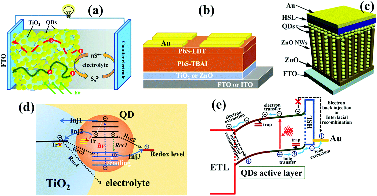 | ||
| Fig. 1 (a) Schematic of sensitized QDSCs. (b) Schematic of planar depleted-heterojunction (PDHJ)-QDSCs. (c) Schematic of bulk depleted-heterojunction (BDHJ)-QDSCs with ZnO nanowires (NWs) and a hole selective layer (HSL). (d) Photoexcited carrier dynamic processes occurring in individual QDs and the sensitized QDSC device, including cooling, injection (Inj), trapping (Tr), and recombination (Rec) of photoexcited carriers. (e) Photoexcited carrier dynamic processes occurring in depleted-heterojunction QDSCs including photoexcited electron and hole transfer or transport in QD solid films, carrier trapping by defects, carrier injection or extraction at the QDs/electrode interface, and interfacial carrier recombination at the QDs/electrode interface. (a) Reprinted with permission from ref. 32. Copyright (2012) American Chemical Society. (c) Reprinted with permission from ref. 33. Copyright (2017) American Chemical Society. | ||
QDSCs convert sunlight energy to electrical energy through a series of complex photoexcited carrier dynamic processes (Fig. 1d and e). After a QD absorbs a photon, an electron will be excited from the valence band (VB) of the QD up to its conduction band (CB), leaving a hole in the VB. Once the photogenerated excitons (electron–hole pairs) are separated successfully, the electron and hole in the QD tend to be transferred to neighbouring QDs or injected into the electron transport layer (ETL) and hole selective layer (HSL), respectively. The photovoltaic performance of QDSCs is mainly determined by the photoexcited carrier (or exciton) generation, carrier extraction, carrier transfer, and carrier recombination processes. Therefore, it is of great importance and necessity to gain a deep insight into those photoexcited carrier dynamic processes in order to further improve the photovoltaic properties of QDSC devices. So far, reviews or analyses on photoexcited carrier dynamics in QDSCs are scarce. Depending on the specialty of research groups, photoexcited carrier dynamics including the photoexcited carrier (or exciton) generation, carrier extraction, carrier transfer, and carrier recombination processes have been investigated in detail by various technologies in QDSCs. Herein, we first focus on the photoexcited carrier dynamics in the entire QDSCs. In sensitized QDSCs, QDs are adsorbed on the surface of semiconductors (e.g. TiO2) with a monolayer, and the main photoexcited carrier dynamics are occurring in a single QD, at the TiO2/QDs interface and photoanode/electrolyte interface, which are shown in Fig. 1d. In PDHJ-QDSCs and BDHJ-QDSCs, different from sensitized QDSCs, the QDs can agglomerate a thick QD light absorbing layer which is made from multiple QD layers rather than a QD monolayer in sensitized QDSCs, thus we have to emphasize both carrier dynamics at the ETL/QDs interface and the additional carrier dynamics in the QD layer (QDs/QDs interface) compared with sensitized devices (only ETL/QDs interface). Another difference from the sensitized QDSCs is that a metal (high work function metal, such as Au and Ag) electrode is used to extract holes from the QDs in DHJ-QDSCs, so carrier dynamics occurring at the QDs/metal electrode interface also need to be discussed. According to the whole process of photoexcited carriers in QDSCs from carrier generation to providing power to the external circuit, we categorize the photoexcited carrier dynamics in the QDSC devices into three main subgroups: photoexcited exciton dynamics in individual QDs, photoexcited carrier dynamics in QD solid films, and interfacial photoexcited carrier dynamics (including carrier transfer and recombination at ETL/QDs interface, photoanode/electrolyte interface and QDs/metal electrode interface) in the solar cell devices. This review puts emphasis on the summary of recent research on photoexcited carrier dynamics in QD and QDSCs, including MEG, hot electron extraction and cooling, surface trapping, carrier transfer and recombination in QD solid films, carrier extraction and carrier recombination at the ETL/QDs interface, photoanode/electrolyte interface and QDs/metal electrode interface and their solutions. We discuss the effects of photoexcited carrier dynamic processes on the physiochemical properties, photovoltaic performance, and eventually the stability of the resulting QDSCs in detail. Simultaneously, we provide our own thoughts on the operating mechanisms and issues encountered with QDSCs.
2. Time-resolved laser spectroscopies for the characterization of photoexcited carrier dynamics
Since the photoexcited carrier dynamics in the QDSCs (Fig. 1d and e) occur in a wide timescale from several femtoseconds (fs) to over milliseconds (ms), it is necessary to employ powerful time-resolved spectroscopic techniques to record these transient carrier dynamic processes.34 Time-resolved laser spectroscopy employs a sub-picosecond or nanosecond pulsed laser as the pump pulse source. After the sample is excited by the pump pulse, a delayed probe pulse or a probe detector is used to monitor how the response signal of the sample has changed with the delay time.35 For example, by changing delay time between the pump and probe pulse in the system path, the photoexcited carrier dynamic processes in the sample can be measured and a time-resolved spectrum can be recorded by using a broadband ultrafast source (e.g. a white light continuum) as probe pulses in transient absorption spectroscopy.13 The time resolution in time-resolved laser spectroscopy is limited by the pulse width of the laser, and the observable timescale range can be adjusted by the electronic auto control of the temporal pump–probe optical delay. The detected information may include absorption or reflection, fluorescence, photoemission, or changes in the linear and non-linear optical response of the sample which depends on the optical path and the probe detector type of the system.36 Thus, the time-resolved laser spectroscopic techniques can provide the quantitative and qualitative determination of the carrier dynamic processes in photoexcited individual QDs, QD solid films or QDSC devices in the range from femtoseconds to over milliseconds.2.1 Transient absorption spectroscopy
Transient absorption (TA) spectroscopy is a particularly versatile type of time-resolved laser spectroscopy for the investigation of the carrier dynamic processes in photochemical and photophysical fields. A schematic diagram of a typical TA spectroscopy measurement using a femtosecond laser source is shown in Fig. 2a. The pump and probe pulses are generated by dividing the output pulse train from an ultrafast laser into two pulses. Both wavelength of the pump and probe pulses can be tuned in a wide range by controlling the set of optical parametric amplifiers (OPA). A white-light probe pulse can also be generated by focusing the output pulse onto a sapphire plate. In TA measurement, the pump-excited changes in the absorption spectrum of the sample are measured as a function of pump–probe delay, and the observable timescale range can be adjusted by the electronic auto control of the temporal pump–probe optical delay. The data are typically presented in the form of normalized differential absorbance (ΔA) which can be defined according to the following equation: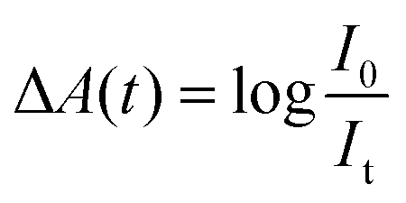 | (1) |
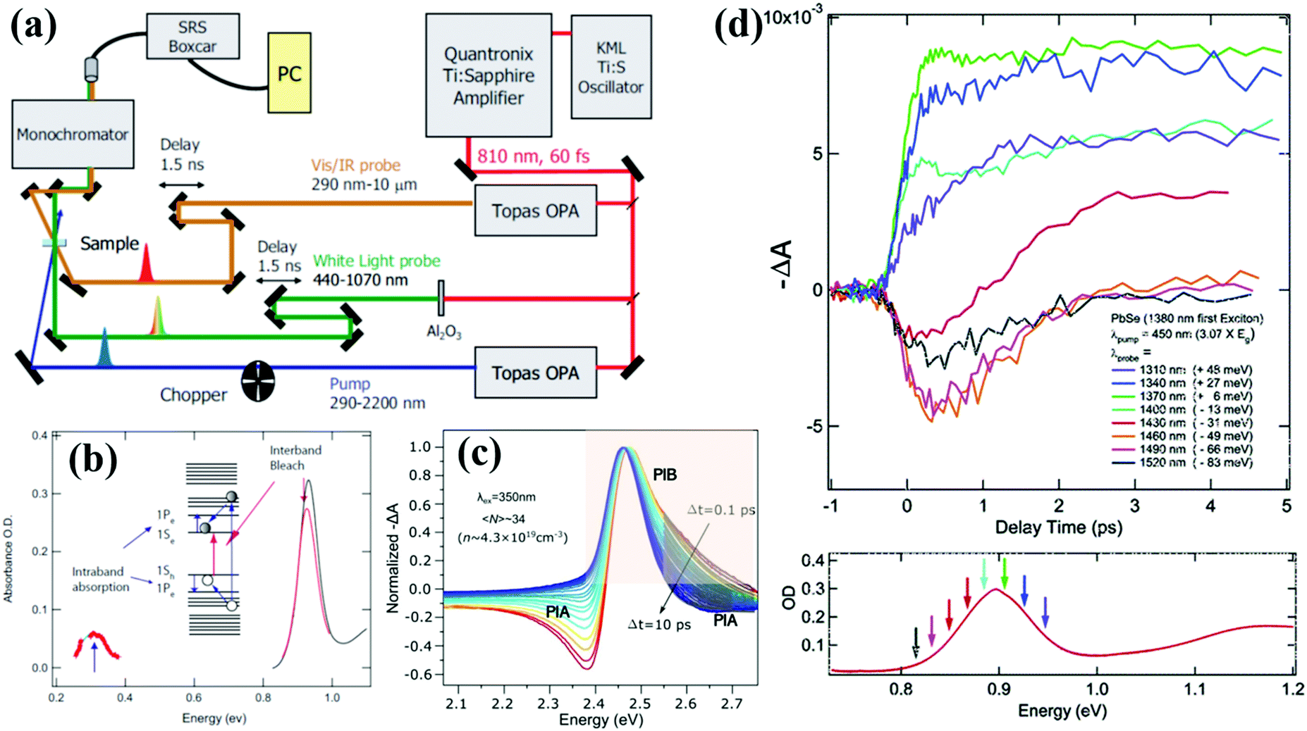 | ||
| Fig. 2 (a) Simplified scheme of a typical TA spectrometer setup. (b) Schematic diagram of the generation for PIB and PIA in TA spectroscopy. (c) Normalized TA spectra of colloidal CsPbBr3 QDs after being excited at short (0.1 ps to 10 ps) pump-pulse delay. (d) Early-time TA data for colloidal PbSe QDs acquired at various probe energies near the 1S exciton energy. (a) and (b) Reprinted with permission from ref. 37. Copyright (2008) Wiley. (c) Reprinted with permission from ref. 41. Copyright (2019) American Chemical Society. (d) Reprinted with permission from ref. 9. Copyright (2005) American Chemical Society. | ||
2.2 Transient grating spectroscopy
Similar to TA spectroscopy, normal transient grating (TG) spectroscopy is an elegant time-resolved laser technique in which the interference of two crossed laser pulses, rather than just one, produces a standing wave of laser intensity and creates a spatially periodic excitation in the sample, and the dynamics of excited species in the sample can be monitored via diffraction of a time-delayed probe beam from the TG. Normally, compared to the TA technique, there are some difficulties to produce the TG using two pulsed pump laser beams and diffract the probe beam from the grating, since these beams need to be simultaneously focused as small spots with diameters of a few 100 micrometers at the same place. Katayama developed a very simple heterodyne TG technique, where only one pump laser beam and a grating is necessary to produce the TG.42–45Fig. 3a presents a schematic diagram of a heterodyne TG method.43 An optical fringe pattern can be formed near the transmission grating when a pulsed pump beam through the grating, and the sample close to the transmission grating can be excited by the fringe pattern. After excitation, the refractive index of the sample is changed due to the complexed photophysical or photochemical processes and the same pattern as the optical fringe will be generated. The pattern of the refractive index change in the sample is called a transient grating. When one probe beam is focused on the transmission grating, a part of the probe beam is transmitted as a reference beam, and the other is diffracted by the transmission grating and then refracted by the transient grating of the sample as a signal beam. A heterodyne signal is established by overlapping the transmitted reference beam with the refracted signal beam whose intensity can be monitored as time passes by.42,43 By using TG spectroscopy, multiple kinds of dynamics in the sample can be observed, such as bulk and surface acoustic waves,46 lattice vibrations,47 phonon scattering and diffusion,48 and carrier relaxation and diffusion (Fig. 3c and d).42,49 Different from TA spectroscopy, a TG signal is obtained from the diffracted beam through the sample, therefore, the sample with no significant light absorption can also be measured by the TG technique. However, since the diffraction angles of different wavelength probe beams are different when they pass through the diffraction grating, they are difficult to focus on the same position of the sample. The probe detector can only record the TG signal decay curve of a single wavelength probe beam with time delay. If we want to get a TG spectrum of the sample, we should change the detector's position and measure the TG decay curves of different probe wavelength beams one by one, and then combine these decay curves into a spectrum, i.e., we cannot get the TG spectrum at the same time (or at the same detector position). In other words, it is difficult to obtain a continuous TG spectrum of the sample at the same point in time.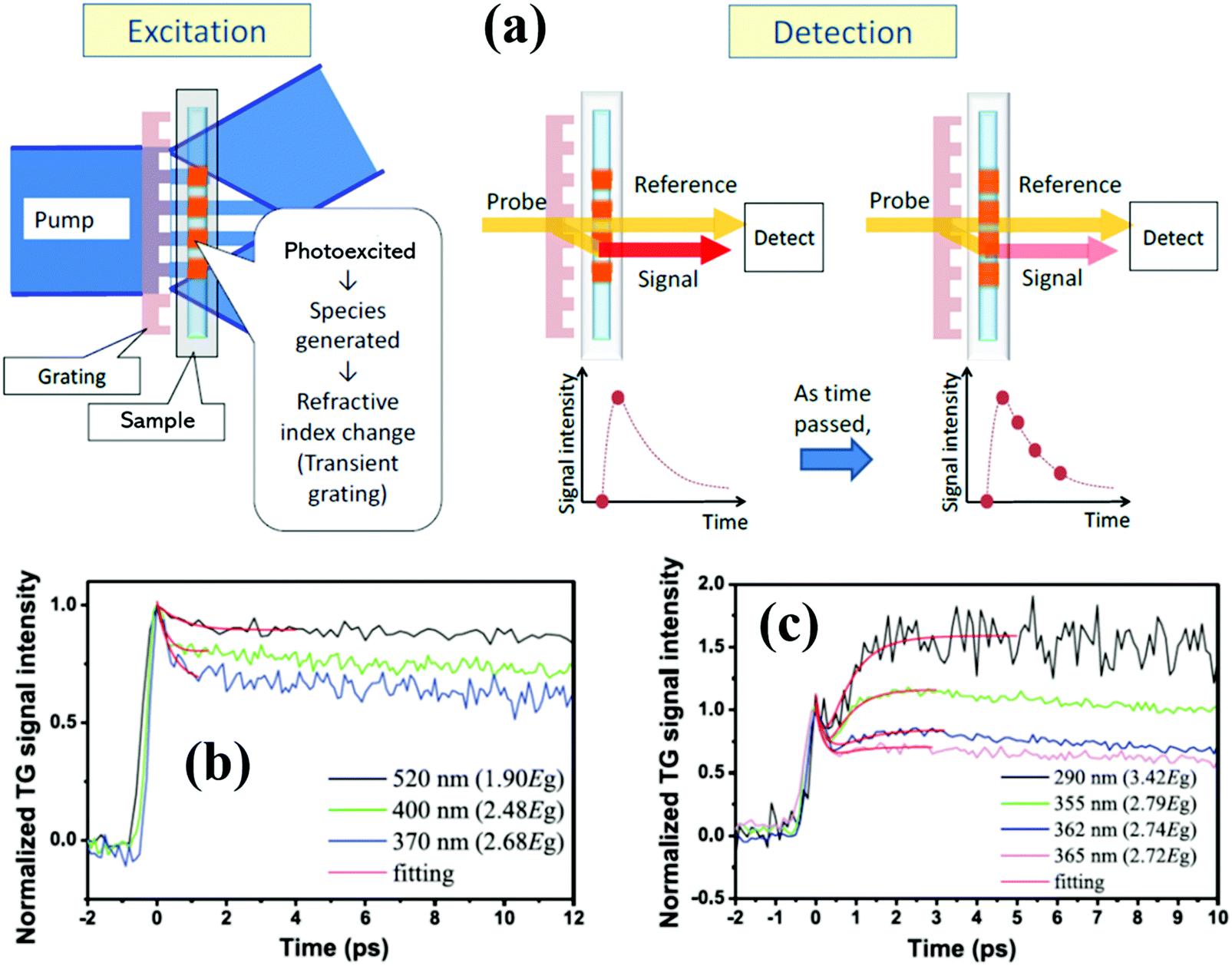 | ||
| Fig. 3 (a) Schematic diagram of the heterodyne TG technique. (b and c) Normalized TG kinetics of the PbS QDs with different pump light wavelengths and their theoretical fitting results. (a) Adapted with permission from ref. 43. Copyright (2013) Royal Society of Chemistry. (c) and (d) Reprinted with permission from ref. 49. Copyright (2015) Elsevier. | ||
2.3 Time-resolved terahertz spectroscopy
Time-resolved terahertz (THz) spectroscopy is a powerful technique to monitor the ultrafast transfer behavior of photoexcited carriers.50 The photoconductivity of a semiconductor will change when an ultrafast pump pulse is used to excite the semiconductor, which will affect the response of the THz signal when THz radiation is used as a probe pulse. The change of photoconductivity (Δσ) in the excited semiconductor can be defined using the following equation:13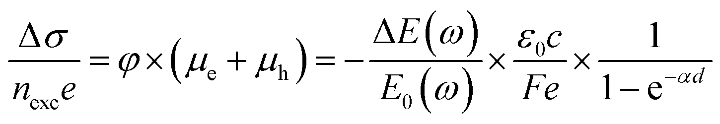 | (2) |
 | ||
| Fig. 4 (a) Simplified scheme of a typical THz spectrometer setup. (b) The photoexcited carrier dynamic curves for the colloidal Si QDs, which are extracted from time-resolved THz spectroscopy (red circles) and TA spectroscopy (blue circles). (c) and (d) are the frequency-resolved THz photoconductivity spectra for the colloidal Si QDs measured at 0.5 ps and 100 ps, respectively. (a) Reprinted with permission from ref. 13. Copyright (2017) American Chemical Society. (b–d) Reprinted with permission from ref. 51. Copyright (2016) American Chemical Society. | ||
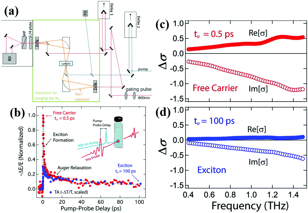
2.4 Time-resolved photoluminescence spectroscopy
Time-resolved photoluminescence (TRPL) spectroscopy is an extension to normal spectroscopy in which an ultrafast laser pulse is used for excitation. Different with TA, TG and THz using probe pulses to monitor the carrier dynamics in the sample, a fast probe detector (CCD camera) is used to determine these excited states which have a radiative decay channel as a function of delay time in the TRPL technique. Different techniques have been employed to measure the TRPL spectra of semiconductors such as direct detection, correlation spectroscopy, and upconversion spectroscopy.36Fig. 5a shows a scheme of the TRPL spectroscopy setup using streak camera-based instrumentation. TRPL spectroscopy can be used to monitor the kinetics of each observed wavelength emission and obtain the dynamic information of photoexcited excitons in QDs such as MEG,52 hot exciton cooling,53 the band to band radiative recombination and the intersublevel thermalization.54 Due to the large timescale differences in the carrier dynamic process, it is important to choose suitable TRPL setups to detect the information about the excited excitons. The time resolution of TRPL spectroscopy is mainly dependent on pulse length of the laser source and the detector system. For detecting the ultrafast photoexcited exciton dynamics such as MEG and exciton relaxation, a Ti:Sapphire laser (pulse length of around 100 fs) together with a streak CCD camera-based TRPL setup is usually used (Fig. 5a). For probing the photoexcited exciton relaxation caused by band to band or interfacial recombination which occurs in a timescale range from several tens of ns up to several ms, a frequency tripled pulsed Nd:YAG laser (pulse length of several ns) and a gated intensified CCD camera are used as an excitation source and detector in the TRPL spectroscopy system, respectively. | ||
| Fig. 5 (a) Scheme of the TRPL spectroscopy setup with streak camera-based instrumentation. (b) Scheme of the TPV spectroscopy setup. (a) Reprinted with permission from ref. 55. Copyright (2014) MDPI. (b) Reprinted with permission from ref. 56. Copyright (2006) American Chemical Society. | ||
2.5 Transient photovoltage decay
The above laser-based TA, TG, TRPL and THz spectroscopy techniques are usually used to monitor the carrier dynamics in colloidal QDs, QD solid films or at the QDs/semiconductor interface. Different from the techniques we discussed above, transient photovoltage (TPV) decay is a popular laser-based opto-electrical technique used to determine carrier recombination dynamics and free carrier lifetime in the solar cell device (Fig. 5b), such as dye-sensitized solar cells, QDSCs and perovskite solar cells. The TPV decay measurement of solar cells is carried out under open-circuit conditions under a steady-state illumination, while an additional high energy laser (or single wavelength light) pulse is applied to the device in order to create a small transient photovoltage. The decay curve of this transient photovoltage records the carrier recombination process in the device (see Fig. 20e, 22f and 23d), and the extracted free carrier lifetime from the decay curve is associated with the steady-state recombination rate of charge carriers within the device.57 Besides that, the recombination processes can also be analyzed based on the effective carrier lifetime (τeff) in the device (see Fig. 21c, f and 23e), which is defined by the following equation:58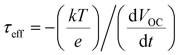 | (3) |
In this section, time-resolved laser spectroscopy which is commonly used to study the photoexcited carrier dynamics in colloidal QD solutions, QD solid films and QDSCs is introduced. These ultrafast laser techniques are powerful tools for us to explain the photo-induced ultrafast physical and chemical phenomena and reactions, and help us explore and discover more unknown phenomena or properties of new materials.
3. Photoexcited exciton dynamics in individual quantum dots
As a core component of QDSCs, quantum dots (QDs) play a decisive role in the photovoltaic performance and stability of the device. Thus, it is of great value to well reveal and understand the photoexcited exciton dynamic mechanism in an individual QD. Fig. 6a shows the photoexcited exciton dynamic processes in an isolated QD. Briefly, after the QD is excited by a photon with an energy larger than the band gap (Eg) of a QD, hot electrons and holes can be formed with excess kinetic energy. The hot electron and hole will be cooling to the bottom of the CB and top of the VB, respectively. During the cooling process, hot electrons and holes will release their excess energy through phonon emission or could excite a new electron from the VB up to the CB if the excess kinetic energy is larger than Eg (called MEG or carrier multiplication (CM) process).59 After cooling, the electron and hole will directly recombine (photoluminescence emission and/or nonradiative emission) or be captured by trap-states which is known as an exciton relaxation process. In this section, the photoexcited exciton dynamic processes in an individual QD are discussed and the recent research in this field is also reviewed.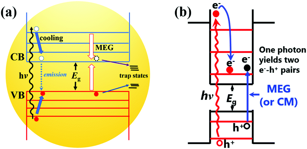 | ||
| Fig. 6 (a) Photoexcited exciton dynamics in an isolated QD. (b) Multiple exciton generation (MEG) processes in QDs. | ||
3.1 Multiple exciton generation
It has been proved that the formation of multiple electron–hole pairs (excitons) following absorption of a single energetic photon can improve the external quantum efficiency (EQE) larger than 100% in the QDSCs and QD-based photoelectrochemical cell.60–62 The generation process of multiple excitons in a semiconductor can be explained by impact ionization (one photon producing multiple excitons).63,64 Impact ionization is difficult to occur in bulk semiconductors due to the necessity of both the momentum conversion and energy conservation. The energy threshold for impact ionization is usually required over four times the band gap (Eg) of the bulk semiconductor, so only UV range (λ < 400 nm) photons can satisfy this demanding condition.65 Similar to impact ionization, MEG (or CM) is a multiple exciton generation process by the excitation of one photon in a quantum confined material (Fig. 6b).65 The CB and VB of the QD are no longer continual, and the quantum confinement and electron–hole Coulomb interaction in the QD are enhanced compared to those of the bulk material.66,67 Thereby, the QD exhibits some new physical properties compared with the bulk such as increased Auger recombination, decreased hot carrier cooling rate and enhanced MEG efficiency (Fig. 7a).68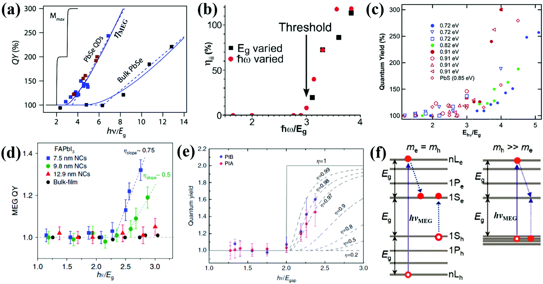 | ||
| Fig. 7 (a) MEG–quantum yield (MEG–QY) for PbSe QDs and bulk. (b) Multiple exciton yield as a function of pump photon energy (ħω). (c) MEG–QY as a function of relative pump photon energies (hν/Eg) for three types of PbSe QDs (Eg = 0.72, 0.82, and 0.91 eV, respectively) and one type of PbS QD (Eg = 0.85 eV), respectively. Solid symbols indicate data acquired using a midinfrared probe, and open symbols indicate band-edge probe energy. (d) MEG–QY as a function of the ratio of hν/Eg for FAPbI3 QDs with different sizes and FAPbI3 bulk film. (e) MEG–QY a function of the ratio of hν/Eg for CsPbI3 QDs. The blue and pink data points correspond to the yield calculated from the photo-induced bleach (PIB) and photo-induced absorption (PIA), respectively. (f) MEG threshold (hνMEG) in QDs. If me = mh, hνMEG is equal to 3Eg. If mh ≫ me, hνMEG can reduce to 2Eg. (a) Adapted with permission from ref. 68. Copyright (2011) American Chemical Society. (b) Reprinted with permission from ref. 71. Copyright (2004) American Physical Society. (c) Adapted with permission from ref. 9. Copyright (2005) American Chemical Society. (d) Reprinted with permission from ref. 70. Copyright (2018) Springer Nature. (e) Reprinted with permission from ref. 93. Copyright (2018) Springer Nature. (f) Adapted with permission from ref. 88. Copyright (2007) American Chemical Society. | ||
There are three characteristics of the MEG property that are generally reported: (1) MEG threshold (hνMEG), which is defined as the required minimum excitation energy to produce MEG in the material; (2) MEG (or exciton)–quantum yield (QY), which is defined as the average number of excitons created in a QD per photon absorbed at a particular photon energy; (3) MEG efficiency (ηMEG), which represents the increment of additional excitons with respect to the increased photon energy beyond the hνMEG. The ηMEG can be obtained from the slope of the MEG–QY vs. hν/Eg plot.69,70 High MEG–QY was observed for the first time in PbSe QDs by Schaller and Klimov in 2004 by using transient absorption (TA) spectroscopy technology.71 They reported an excitation energy threshold for the formation of two excitons per photon at 3Eg, and MEG–QY as high as 218% was observed for photon energy of 3.8Eg (Fig. 7b). Then, Ellingson et al. confirmed this report of efficient MEG in PbSe QDs.9 300% MEG–QY exciting at a photon energy of 4Eg in PbSe QDs is observed, which indicates that one photon can generate an average of three excitons in PbSe QDs (Fig. 7c). A new model for MEG based on the coherent superposition of multiple excitonic states is introduced, and they provided evidence that the excitation energy threshold for MEG could reduce to 2Eg. In addition, a comparably efficient MEG is also found for the first time in PbS QDs (see Fig. 7c). In recent years, TA spectroscopy72–77 and other ultrafast time-resolved spectroscopy including time-resolved photoluminescence (TRPL),52,78,79 transient grating (TG),49,80,81 and transient terahertz (THz)51,82 were carried out to confirm efficient MEG in PbSe and PbS QDs.83 Besides, the MEG phenomenon has been detected in other QDs, such as PbTe,61,84 CdSe,85–87 InAs,88 InP,89 PbSe/CdSe core/shell,90 PbS/CdS Janus-like heterostructure QDs,91 halide perovskites (ABX3) like MAPbI3 (MA = CH3NH3),92 FAPbI3 [FA = HC(NH2)2] (Fig. 7d),70 and CsPbI3 (Fig. 7e),93 and indirect bandgap semiconductors including Si and Ge.69,94–97 Here we summarize the reported MEG property for several QDs in Table 1. Although the QDs have the same composition with similar bandgaps, their reported MEG property exhibits large difference mainly due to the different measurement conditions (containing stirring or static solutions) and surface chemistry. In QDs, the hνMEG relates to the effective electron mass (me) and hole mass (mh), and their relationship equation (assuming that mh ≥ me) is hνMEG = (2 + me/mh)Eg.85 Thus, the larger difference of hνMEG between different QD materials is mainly due to their distinct ratio of me/mh. In addition, the Coulomb exciton–exciton interaction energy in QDs can reduce the hνMEG below the apparent minimum of 2Eg.88 In the experimental studies of MEG, a usually observed “MEG-like” fast decay signature is mainly caused by the degradation of surface passivation or QD charging effect due to QD photoionization.98 The former can result in new decay paths due to trapping at surface defects,99 while the latter can produce extraneous “MEG-like” decay components.100 These results indicate that surface trap-states and surface chemistry of QDs may largely affect the MEG process.100,101 The specific influence of surface ligands and surface passivation on the properties of QDs will be further discussed in more detail below.
| Material | α B (nm) | m e/mh (m0) | E g (eV) | hν MEG (eV) | E hv /Eg | MEG–QY (%) | η MEG | IQE/EQE | Ref. |
|---|---|---|---|---|---|---|---|---|---|
| PbS | 20102 | 0.085/0.085103 | 0.85 | 2Eg | 4 | 160 | — | — | 9 |
| 0.99 | 3Eg | 3.1 | 102 | 0.40 | — | 104 | |||
| 1.25 | 2.7Eg | — | — | — | — | 49 and 80 | |||
| 0.85 | 2.7Eg | 3.83 | — | — | —/118% | 62 | |||
| PbSe | 46102 | 0.084/0.07105 | 0.94 | 3Eg | 3.8 | 218 | — | 71 | |
| 0.91 | 2Eg | 4 | 300 | — | — | 9 | |||
| 0.72 | 2.8Eg | 4.86/3.26 | — | 0.62 | 130%/114% | 60 | |||
| 0.89 | 2.8Eg | 3.7 | 120 | 0.41 | — | 104 | |||
| PbTe | 15284 | 0.031/0.036106 | 0.90 | 2.6Eg | 4 | 300 | — | — | 84 |
| 0.95 | 2.9Eg | 3.47 | — | — | 150%/122% | 61 | |||
| CdSe | 6102 | 0.13/0.45107 | 2.0 | 2.5Eg | 3.1 | 165 | — | — | 85 |
| InAs | 34102 | 0.023/0.42103 | 1.31 | 2Eg | 2.74 | 120 | — | — | 88 |
| InP | 10108 | 0.078/0.40109 | 2.0 | 2.1Eg | 2.6 | 118 | — | — | 89 |
| FAPbI3 | 6.270 | 0.14/0.2070 | 1.71 | 2.25Eg | 2.7 | 132 | 0.75 | — | 70 |
| CsPbI3 | 6110 | 0.15/0.20111 | 1.77 | 2Eg | 2.4 | 160 | 0.98 | — | 93 |
| Si | 4.997 | 1.18/0.81112 | 1.22 | 2.4Eg | 3.4 | 260 | — | — | 97 |
| 1.55 | 2Eg | 2.7 | 200 | — | — | 96 | |||
| Ge | 24.3113 | 0.12/0.11114 | 1.25 | 1.6Eg | 2.8 | 190 | — | — | 95 |
3.2 Hot electron extraction and cooling
In QDs, the energy levels are not continual and the energy difference between two adjacent energy levels can be larger than its bandgap (Eg). When the energy of the incident photon is larger than Eg, hot excitons with excess energy are generated in QDs. After generation, the fate of the hot excitons will take three paths (Fig. 8): (1) hot exciton dissociation via hot electron (or hole) transfer to or be extracted by an adjacent electron (or hole) acceptor; (2) hot excitons dedicate their excess energy to electrons in the VB and could generate one or more new excitons in internal QDs, this process is known as MEG which we have introduced above; (3) hot excitons can be cooled to the lowest energy state and release their excess energy to phonons. In an isolated QD, the number of excitons generated per absorbed photon (the MEG–QY or QYMEG) can be expressed by the following equation:115 | (4) |
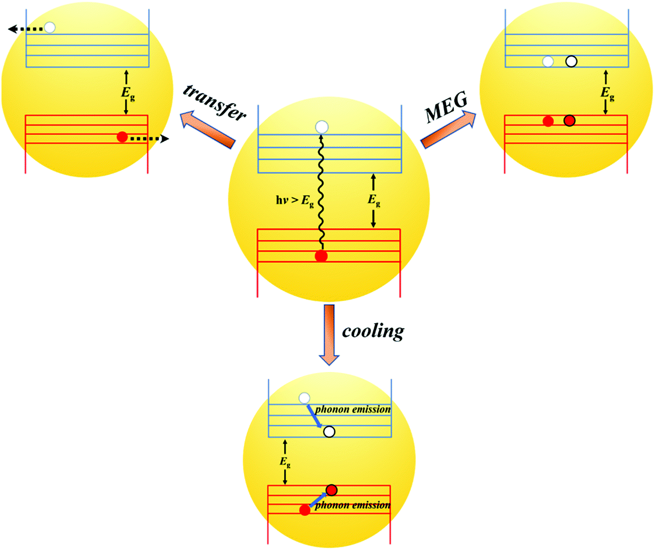 | ||
| Fig. 8 The dynamic processes of hot excitons in individual QDs. | ||
The study of hot electron and hole extraction from QDs has been going on for decades. In order to investigate the fast electron and hole extraction process, researchers used molecular adsorbates as electron and hole acceptors to extract hot electrons and holes from the QD.117,118 Because the hot electron cooling is slower than hot holes in many QDs, the extraction is much more efficient for hot electrons than for hot holes.119 Therefore, the extraction or transfer behavior of hot electrons at the ETL/QDs and QDs/QDs interface is stated in detail.
Tisdale et al. have reported hot electron transfer from PbSe QDs to single crystalline (110) TiO2 for the first time using a time-resolved optical second harmonic generation (SHG) technique.120 The hot electrons can transfer from PbSe QDs (sizes from 3.3 to 6.7 nm) to TiO2 in 50 fs, even though the lowest excited electronic state of the QDs is lower than the CB minimum (CBM) of TiO2. Since the size and surface ligand of the QD play an important role in affecting the relative band alignment (ΔG) and the interfacial electronic coupling between the QD and electron acceptor (i.e. TiO2),121 the hot electron extraction and cooling behaviors at the TiO2/PbSe QD interface are mainly determined by the size of the PbSe QDs as well as the surface ligand types. The photoexcitation of the PbSe QDs leads to a decrease (or drop) in SHG signal intensity if no electron transfer occurs, but in contrast, the rise in SHG signal intensity corresponds to electron transfer from the PbSe QDs to TiO2. Thus, PbSe QDs treated with 1,2-ethanedithiol (EDT) display efficient hot electron extraction for all sizes studied, whereas substantial hot electron extraction is only observed for hydrazine (HYD) treated PbSe QDs with a smaller size (Fig. 9a). Meanwhile, hot electron extraction probability is reduced due to the enhanced hot electron cooling process with the measurement temperature increasing (Fig. 9b). Recently, Wang et al. observed that the measurement temperature could also affect a hot electron extraction process in SnO2/PbS QD sensitized systems.122 PbS QDs are nucleated directly onto SnO2 nanoparticles by a successive ionic layer adsorption and reaction (SILAR) method, and the hot electron transfer rate and efficiency are quantified by using THz spectroscopy. When the temperature is reduced from 293 to 135 K, the hot electron extraction efficiency increases from 70% to 90%, while the temperature-dependent hot electron transfer rate rises from about 2 × 10¹² to over 4 × 10¹² s−1 which is in good accordance with the corresponding temperature-dependent hot electron extraction efficiency trend (Fig. 9c and d). It needs to be mentioned that hot electron extraction in PbS QD-sensitized mesoporous SnO2 can be observed at room-temperature for the first time in their work. This result confirms that the extraction of hot electrons in QDSCs at room temperature is very promising. The pump energy and QD size-dependent hot electron extraction behavior at the SnO2/PbS QD interface has also been investigated. The hot electron transfer rate has an exponential relationship with the excess energies [Eex = (hν − Eg)/2] of hot electrons below 0.6 eV, and a linear relationship when Eex is over 0.6 V. (Fig. 9e). Moreover, larger PbS QDs have faster hot electron transfer rate and higher extraction efficiency than the smaller QDs (Fig. 9f). Cánovas et al. employed THz spectroscopy to evaluate hot electron transfer which takes place from the 1Pe state of PbSe QDs to the conduction band (CB) of mesoporous SnO2 and TiO2 films with 3-mercaptopropionic acid (3-MPA) as a ligand.123 The hot electron transfer from the 1Pe state of the PbSe QDs to the CB of TiO2 is efficient at room temperature (∼80%), while the efficiency towards SnO2 is almost null. Higher hot electron extraction efficiency at the TiO2/PbSe QDs interface than that of the SnO2/PbSe QDs interface is mainly due to the stronger donor–acceptor coupling effect between TiO2 (electron acceptor) and PbSe QDs (electron donor) which finally helps electron transfer to win the kinetic competition with electron cooling.
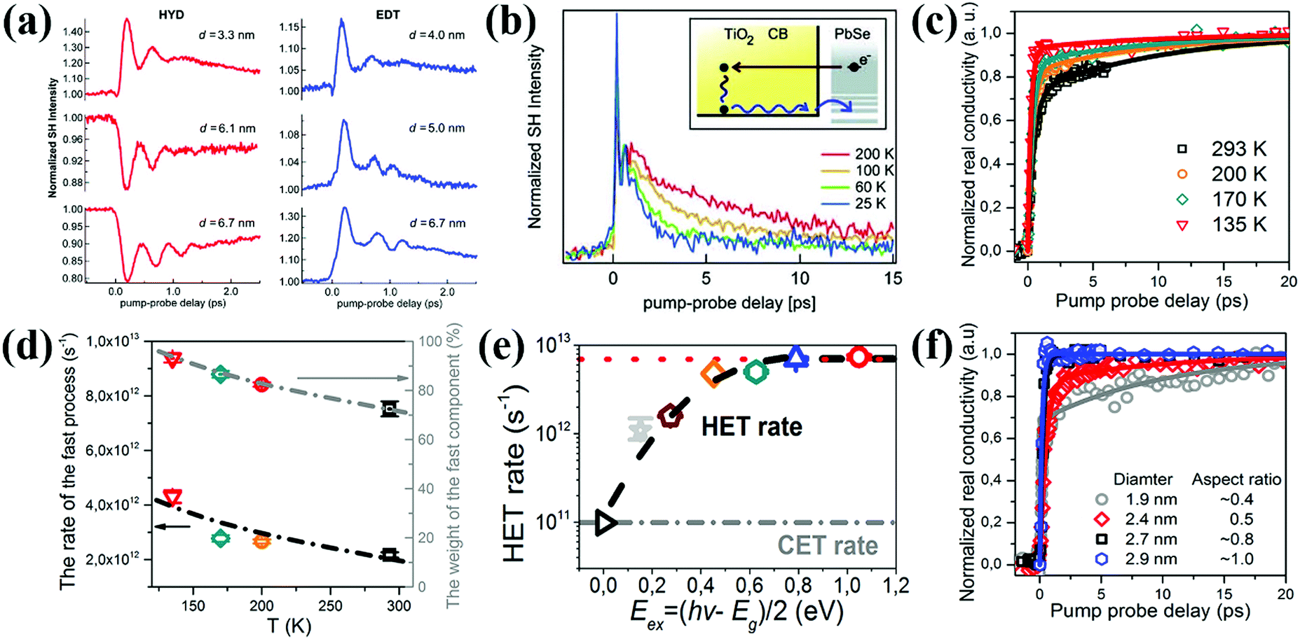 | ||
| Fig. 9 (a) HYD and EDT treated PbSe QD size dependent time-resolved second harmonic response. (b) Temperature-dependent decay of the pump induced SHG signal enhancement. (Inset) Electron dynamic process at the TiO2/PbSe QD interface. (c) Temperature-dependent hot electron dynamics in the SnO2/PbS QD interface following 400 nm excitation. (d) Temperature-dependent hot electron transfer rates and efficiency at the SnO2/PbS QD interface. (e) Hot electron transfer (HET) rates and cold electron transfer (CET) rates vs. the excess energies of hot electrons. (f) PbS QD size-dependent electron transfer dynamics at SnO2/PbS QD interfaces following 400 nm excitation. (a and b) Reprinted with permission from ref. 120. Copyright (2010) AAAS. (c–f) Reprinted with permission from ref. 122. Copyright (2018) American Chemical Society. | ||
Using TA spectroscopy, Lian and co-workers did a series of works to accelerate electron extraction from QDs by introducing molecular adsorbates as electron acceptors.73,124–129 Subsequently, they utilized benzoquinone (BQ) and phenothiazine (PTZ) as electron and hole acceptors to investigate both the electron and hole extraction properties of CsPbBr3 perovskite QDs.130 The measured electron transfer and hole transfer half-lives are 65 ± 5 ps and 49 ± 6 ps, respectively. With the same strategy, Sarkar et al. observed an efficient hot electron and hole transfer of CsPbBr3 QDs occurring in the sub-300 fs time scale.131 The hot electron and hole transfer rates are much faster than the Auger recombination (about 20–40 ps), and the transfer of thermalized electrons and holes are also observed with characteristic time constants of 30–50 ps and 196–250 ps, respectively. Compared with MAPbBr3 bulk film, approximately two-times slower hot carrier cooling time (∼18 ps) is detected in MAPbBr3 QD solution due to the intrinsic phonon bottleneck effect and Auger heating effect of QDs.132 Profitting from the slow hot carrier cooling behavior of MAPbBr3 QD, Li et al. used a molecular semiconductor named 4,7-diphenyl-1,10-phenanthroline (Bphen) as a hot electron acceptor to successfully extract about 83% of hot electrons from MAPbBr3 QD solid film within 1 ps at room-temperature.132 In recent years, hot electron and hole transfer behaviors in core/shell QD and QD heterojunction films were also investigated.133–136 Although a fast hot carrier extraction process in these systems can be observed, hot electrons and holes are difficult to transport to the electrode or quickly transferred back to the donor due to the stringent energy level requirement between donor and acceptor for hot carrier extraction.
Photoexcited hot excitons can be relaxed to the states at the band edge by releasing their excess energy as a phonon to the lattice. This undesired hot exciton cooling process severely limits the efficiency of photovoltaic devices. As a kinetic competitor of hot electron or hot hole extraction processes, the hot exciton cooling process is expected to be slower which may leave time to extract the energy of hot excitons for more efficient solar cells.8 The hot exciton cooling process can be considered as the excitonic state-to-state transition process which is affected by the exciton–phonon coupling and surface trapping effects of QDs.137,138 Pandey et al. firstly reported slow hot electron cooling in colloidal QDs.139 The hot electron cooling time between 1Se and 1Pe of small CdSe QDs can be tuned from less than 6 ps to more than 1 ns by controlling the size of CdSe QDs and the thickness of a ZnSe passivation layer, which is slower than the reported hot electron transfer time. This result validates that extracting hot electrons from QDs to improve the efficiency of QDSCs is feasible. In early research, the cooling rates of electrons and holes have often been assumed to be equal. Actually, as the effective mass of the electron is usually smaller than that of the hole in QDs, especially for III–V semiconductor QDs, the electron level spacing is generally greater than that of the hole in those QDs.140 This special band structure may lead to increased hole cooling rate compared to electron cooling rate.119 Spoor et al. firstly investigated the separate hot electron and hole cooling behaviors in PbSe QDs by using hyperspectral TA spectroscopy.119 More importantly, the hole cooling in PbSe QDs is much faster than electron cooling at all excitation energies, and the same phenomenon was found by decreasing the PbSe QD size from 4.8 nm to 3.9 nm. This is the first report to establish a broadband hot exciton cooling spectrum in QDs, which is very useful to understand and control the hot exciton cooling behavior in QDs.141
3.3 Surface trap-induced recombination and solution strategy
Photogenerated electrons and holes are very easy to be caught by trap-states before they’re extracted or relaxed via band to band recombination. Thus, the trap-state density in QDs has an adverse effect on the photoexcited carrier dynamic processes in QDSCs, such as MEG and photoexcited carrier extraction. Compared with bulk materials, QDs have a higher surface to volume ratio. As this ratio increases, the properties of the surface atoms will dominate the properties of the entire QD. The surface atoms of QDs have unbonded orbitals which are thought to be the origin of charge trapping states.142–144 These surface states are the trap centers of photogenerated electrons and holes, and play a critical role in determining the properties of QDs such as stability, photoluminescence (PL),145 defect energy levels etc. Surface passivation through a core/shell strategy or ligand engineering of QDs is confirmed to be an effective way to reduce the QD's surface trap-state density and avoid its oxidation.146–150Hines et al. firstly reported a wet chemical technology to synthesize CdSe@ZnS core/shell structure colloidal QDs in 1996 via a two-step single-flask process.151 Thin monolayer ZnS (∼0.6 nm) can reduce the surface defects and enhance the PL quantum yield (PLQY) as well as the stability of CdSe QDs. Zhong and co-workers then introduced a thin ZnS layer as a passivation layer to synthesize ‘‘green’’ CuInS2/ZnS core/shell QDs through a cation exchange approach.152 The average lifetime (τav) of photoexcited excitons is increased from 355 ps to far larger than 1 ns after ZnS passivation on the CuInS2 QD surface (Fig. 10a–c). This result indicates that the surface trap-states on CuInS2 QDs decrease significantly after ZnS passivation. While the ZnS layer also acts as a barrier layer for electron injection from the QDs to the TiO2 electrode leading to a reduced electron injection rate constant (ket), which we will introduce in Section 5.1. In addition to ZnS,153 CdS,154–157 ZnSe,158 CdSe,159 and Al2O3160etc. can be employed as a shell or passivation layer to protect QDs from oxidation and reduce their surface trapping states. The core/shell strategy has been confirmed to be beneficial for reducing the surface trap-state density and improving the chemical stability of the core QD.161 Furthermore, photoexcited carrier dynamic processes in QDSCs can be tuned via the energy level alignment of the core and shell of the QD.162
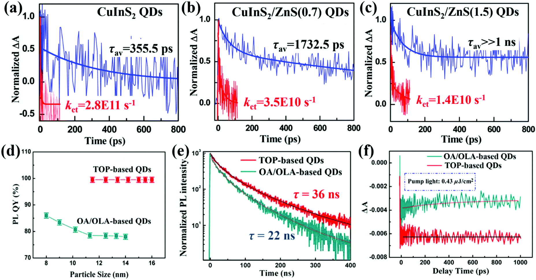 | ||
| Fig. 10 TA response curves of (a) bare CuInS2 QDs, (b) CuInS2 QDs with a 0.7 monolayer ZnS shell, and (c) CuInS2 QDs with a 1.5 monolayer ZnS shell deposited on SiO2 (blue line) and TiO2 substrates (red line). All samples were pumped by a 388 nm laser pulse and probed at 580 nm. Since electrons cannot inject from QDs to the insulating SiO2, the TA decay curve indicates the carrier recombination in the QDs including through surface trap-states (fast process) and direct band to band recombination (slow process). The value of ket was calculated by the equation: ket = 1/τav(QDs/TiO2) − 1/τav(QDs/SiO2). (d) PLQYs of the TOP-based and OA/OLA-based CsPbI3 QDs with different particle sizes. (e) TRPL decay curves of the TOP-based and OA/OLA-based CsPbI3 QD solutions with excitation wavelength of 532 nm (pump fluence 0.9 μJ cm−2) and a probe light wavelength of 685 nm. (f) TA response of the TOP-based and OA/OLA-based CsPbI3 QD solutions measured with a pump light wavelength of 470 nm (pump fluence 0.43 μJ cm−2) and probe light wavelength of 670 and 650 nm, respectively. (a–c) Reprinted with permission from ref. 152. Copyright (2014) American Chemical Society. (d–f) Reprinted with permission from ref. 164. Copyright (2017) American Chemical Society. | ||
Surface ligand plays a key point in influencing the trap-state density and quality of QDs in the synthesis process of QDs, especially ligand type and amount.163–165 In our recent work, trioctylphosphine (TOP) is used as a solvent and ligand to synthesize highly crystalline and low defect density CsPbI3 QDs with a near 100% PLQY (Fig. 10d).164,166 Longer PL lifetime is obtained for CsPbI3 QDs by using a TOP-based strategy (36 ns) than those obtained by using oleic acid (OA)/oleylamine (OLA) mixture ligands (22 ns) (Fig. 10e), implying that the TOP-based strategy significantly reduces the nonradiative recombination centers on the surface of the CsPbI3 QDs. The no recovery (in 1 ns time scale) of TA bleaching for TOP-based CsPbI3 QDs also confirms that the trap-states on the surface of CsPbI3 QDs are almost completely suppressed (Fig. 10f). A PCE of 12.15% is achieved for the QDSCs based on these CsPbI3 QDs and it can retain 85% of the peak value after storage in air over 90 days.166 Woo et al. reported a new surface ligand tris(diethylamino)phosphine (TDP) containing “P–O–” moiety as a Se source in the form of TDPSe to replace the commonly used Se precursor trioctylphosphine selenide (TOPSe) during the synthesis process of PbSe QDs.167 TDP ligand can be anchored on the PbSe QD surface through the “P–O–” bond and the use of TDPSe as a Se precursor results in drastically enhanced air stability of PbSe QDs even when the QDs are exposed to air for weeks compared with TOPSe. The same result was obtained when changing TDP to other phosphonic acids such as hexylphosphonic acid (HPA), tetradecylphosphonic acid (TDPA), and octadecylphosphonic acid (ODPA).
Nowadays, injecting halide ligand precursors into QD solutions during the end stages of the synthesis process has been found to be effective to reduce the surface trap-state density on QDs.168,169 Tang et al. used a CdCl2 precursor solution containing CdCl2, TDPA and oleylamine (OLA) to passivate PbS QDs.169 After CdCl2 passivation, the size distribution of the PbS QDs is improved, the surface trap-state density is reduced and the stability of the PbS QDs is also improved. For the purpose of passivating the surface of PbS QDs and reducing the surface trap-state density, Ning et al. reported a solution-phase halide passivation method by adding tetrabutylammonium iodide (TBAI) salt/OLA complex into the PbS QD toluene solution.170 The absolute PLQY of the TBAI-treated PbS QDs is 1.7 times higher than that of the untreated QDs, and the density of trap-states of the TBAI-treated PbS QDs is much lower than that of the untreated ones (Fig. 11a). After passivation, the electron mobility of the QD solid film, which can be obtained from the QD solid film based field-effect transistor (FET) device, is also significantly improved. Subsequently, Azmi et al. used 1-propyl-2,3-dimethylimidazolium iodide (PDMII) salt/OLA complex solution exhibiting n-type behavior as the iodide source to passivate the surface of PbS QDs during a solution-phase iodide treatment procedure.171 The PLQY values of the pristine PbS, TBAI-treated PbS, and PDMII-treated PbS QDs in octane solutions are 19%, 23%, and 27% respectively. This indicates that PDMII as an iodide source is more efficient than TBAI for the surface passivation of PbS QDs. Molecular iodine (I2) is also employed as an iodide source to passivate the surface trap-states in the as-synthesized PbS QDs via an anion exchange reaction between PbS and I2.172 After I− passivation, the PLQY of the PbS QDs is improved from 15% to 19% and a twofold decrease in trap-state density is observed in the I−-treated PbS QD solid film, which results in a certified PCE of 9.9%. Unfortunately, the highly reactive nature of molecular iodine can lead to uncontrolled fusion of PbS QDs.173 In order to better balance the competition between iodine passivation and dispersion of PbS QDs, a milder ionic iodine source, methylammonium iodide (MAI), is employed to passivate the surface of the PbS QDs.173 Following the MAI treatment, the PLQY of the PbS QD solution has increased from 15% to 29%, whereas the I− treatment achieves an increase to only 19%.
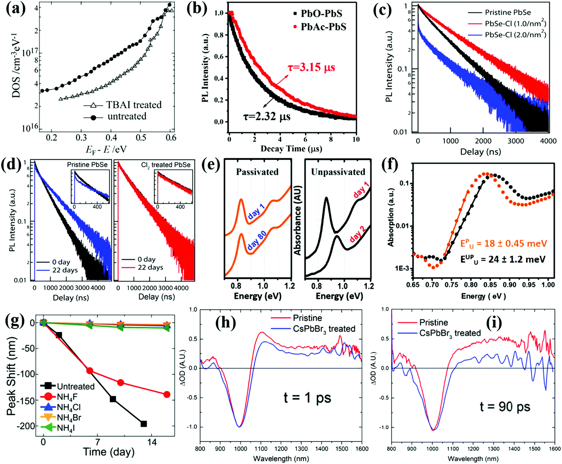 | ||
| Fig. 11 (a) Density of trap-states in PbS QD solid films made using solution-phase TBAI treated QDs (triangle) compared with untreated QDs (dot). (b) TRPL decay curves of PbO-PbS QDs and PbAc-PbS QDs in solution. (c) TRPL decay dynamics of PbSe QDs with varied Cl2 concentrations. Heavy Cl2 treatment (2.0 nm−2) leads to the formation of new trap-states, possibly arising at the PbSe/PbClx interface. (d) TRPL decay traces of pristine (left panel) and chlorine-treated (right panel) PbSe QDs after 22 days of oxygen exposure. (e) Absorption spectra of passivated (orange) and unpassivated (black) PbSe QD solid films after storage in air. (f) Photothermal deflection spectra of unpassivated (black) and passivated (orange) PbSe QD solid films. Solid lines represent the linear fit of the slope. The calculated EU for PbSe QDs solid film is listed. (g) Absorption peak shifts of untreated PbSe QDs and halide treated PbSe QDs with various NH4X (X = F, Cl, Br, I). (h) The TA spectra of the pristine and CsPbBr3-treated PbSe QDs at t = 1 ps. (i) The TA spectra of the pristine and CsPbBr3-treated PbSe QDs at t = 90 ps. (a) Reprinted with permission from ref. 170. Copyright (2012) Wiley. (b) Reprinted with permission from ref. 176. Copyright (2018) Wiley. (c and d) Reprinted with permission from ref. 178. Copyright (2012) American Chemical Society. (e and f) Reprinted with permission from ref. 177. Copyright (2014) Wiley. (g) Reprinted with permission from ref. 179. Copyright (2014) American Chemical Society. (h and i) Reprinted with permission from ref. 180. Copyright (2017) Wiley. | ||
Cademartiri et al. and Zhang et al. synthesized in situ halide-passivated PbS QDs by using lead halide precursors which demonstrated higher PLQYs and better stability compared to the conventionally synthesized QDs using PbO as the precursor.174,175 Based on this, Wang et al. successfully synthesized PbS QDs by using a lead precursor lead acetate trihydrate (PbAc2·3H2O) with PbO as a reference.176 The acetate ligands present in situ passivation on the surface of PbS QDs. The PbS QDs synthesized from PbAc2·3H2O (PbAc-PbS) exhibit higher PLQY (15.08%) compared with PbO (PbO-PbS) based ones (10.05%). And the PL lifetime of the PbAc-PbS QDs (3.15 μs) is longer than that of PbO-PbS QDs (2.32 μs) from the result of time-resolved photoluminescence (TRPL) decay as well (Fig. 11b), which indicates that the surface trap-state density in the PbAc-PbS QDs is lower than that of PbO-PbS QDs.
Compared with PbS QDs, PbSe QDs are more vulnerable to be oxidized due to lower electronegativity of selenium than sulfur,177 thus generally surface passivation is more critical for PbSe QDs. Bae et al. used a solution phase passivation method to reduce the surface trap-state density and improve the stability of PbSe QDs via a reaction with molecular chlorine (Cl2).178 The Cl− passivation reaction is carried out at room temperature by slowly adding a small amount of a 10 mM solution of Cl2 in CCl4 to a stirred sample of PbSe QD dispersed in toluene. Cl− can preferentially take the place of surface Se ions on PbSe QDs and can be reacted with Pb ions to generate a thin PbClx passivation layer. After Cl− treatment, the PL lifetime in the PbSe QDs is increased, indicating a reduction in nonradiative recombination caused by surface trap-states (Fig. 11c), while the PbClx passivation layer can effectively prevent the oxidation of QDs during long-term air exposure (Fig. 11d). Asil et al. introduced a CdCl2–TDPA–OLA mixture into the PbSe QD solution at the end of the growth period.177 The stabilities of both the PbSe QD solution and PbSe solid film are improved after Cl− passivation (Fig. 11e). The Urbach energy (EU) of the passivated PbSe QD solid film is smaller than that of the unpassivated PbSe QDs due to the suppressed carrier trapping and reduced energetic disorder (Fig. 11f). Besides chlorine, other halide ions also exhibit the performance to reduce the surface trap-state density of QDs. Woo et al. synthesized halide-treated ultrastable PbSe QDs by adding different types of halide salt methanol solution into the reaction solution after the QD growth stopped.179 Nearly all NH4X (X = F, Cl, Br, I) salts except fluoride (F) can well protect PbSe QDs (Fig. 11g). Chloride salts with various cations such as NaCl, KCl, and InCl3, as well as bromide salts such as NH4Br, cetyltrimethylammonium bromide (CTAB) and tetrabutylammonium bromide (TBABr) are almost equally effective in stabilizing PbSe QDs. Confirmed with the result from Bae et al.,178 it is found that after halide treatment, an atomically thin PbX2 (X = Cl, Br, I) adlayer can be formed on the top of the PbSe(100) surface which is much less prone to oxidation than Se, which can protect the PbSe surface from being oxidized. Huang et al. then reported a solution-phase method to passivate the surface of PbSe QDs using CsPbBr3 or CsPbI3 nanoparticles (NPs) as a halide source.180,181 The original Cl− on the surface of PbSe QDs can be replaced by the halide ions from the CsPbX3 NPs and finally forms hybrid Cl/Br or Cl/I passivated QDs, which reduces the surface defects on the PbSe QDs and improves the PLQY of the PbSe QDs in solution. The TA spectroscopy signal of the PbSe solid film is consistent with the result of PLQY measurement. Generally, the photoexcited excitons in QDs can be captured by surface trap-states which induces the enhanced positive photoinduced absorption (PIA) signal in the longer wavelength region of the TA spectrum.99,182 The solid film made by pristine PbSe QDs shows a strong PIA signal over time, while the PIA signal of the solid film made by CsPbBr3-treated PbSe QDs is significantly decreased (Fig. 11h and i), indicating that CsPbX3 treatment can effectively reduce the density of surface trap-states on the PbSe QDs.
The recent studies of photoexcited exciton dynamics in individual QDs are summarized in Section 3, MEG and hot electron extraction have been observed in many semiconductor QDs. Unfortunately, only a few reported QDSCs devices achieved over 100% EQE but only in the UV region.60,61 Hot excitons are difficult to be extracted before their cooling or trapping in most QDs. Thus, new narrow bandgap QD semiconductors or quasi-type-II core/shell structure QDs with visible light MEG response and slow hot exciton cooling rate need to be explored and investigated in the future.90 Novel QD surface passivation strategies, such as halide-based hybrid ligand systems, should also be developed to reduce the surface trap-state density of QDs, achieve as high as 100% PLQY, and elongate the lifetime of hot excitons.
4. Photoexcited carrier dynamics in quantum dot solid film
The photoexcited excitons in an individual QD as mentioned above ought to be efficiently extracted or transferred to its neighbors before trapping or recombination so as to achieve electron and hole effective separation (or exciton dissociation). Thus, exciton dissociation behavior in adjacent QDs or in QD solid film is crucial in affecting the performance of QDSCs, especially for the depleted-heterojunction structure QDSCs. Generally long chain insulating organic ligands must be replaced by short conduction ligands for the integration of individual QDs into solid films with tunable electronic properties. In a recent study, the surface ligand had a significant impact on the properties of QD solid films, such as band structure (Fig. 12a),183,184 doping density (Fig. 12b),185,186 carrier mobility and diffusion length (Fig. 12c).187,188 Thus, the surface ligand of the QDs plays a core role in enhancing the electronic properties of the QD solid film and photovoltaic performance of QDSCs.189,190 In this section, we summarize the latest research in QD surface engineering, with our focus on those that have demonstrable contribution to affecting photoexcited carrier dynamics in QD solid films and the resulting photovoltaic performance of QDSCs.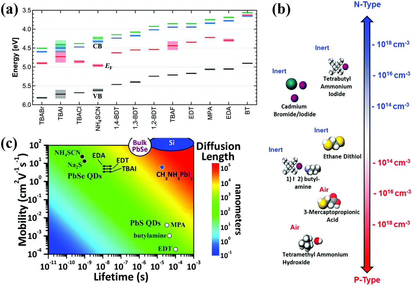 | ||
| Fig. 12 (a) Energy level diagrams of PbS QD solid films treated with various ligands. (b) Illustration of the doping type of various ligands for PbS QDs. Organic ligands in air result in p-type doping and halide ligands bring n-type doping. (c) Carrier mobilities and diffusion lengths of PbS and PbSe QD solid films treated with various ligands. (a) Reprinted with permission from ref. 183. Copyright (2014) American Chemical Society. (b) Reprinted with permission from ref. 185. Copyright (2012) American Chemical Society. (c) Adapted with permission from ref. 187. Copyright (2015) American Chemical Society. | ||
In the QD solid film, photogenerated excitons can be usually relaxed via radiative recombination and non-radiative recombination paths. The relaxation of excitons through the radiative recombination path usually occurred in the individual QDs (Fig. 8). The non-radiative recombination processes in QD ensembles mainly contain: (i) exciton dissociation (i.e. photoexcited electron and hole transfer) between adjacent QDs, (ii) photoexcited carrier trapping through inner and/or interfacial defects, and (iii) energy transfer in disordered QDs (Fig. 13a).191 The exciton dissociation process (i) in QD solid films is usually dependent on the QD–QD interparticle distance, the photoexcited carrier trapping process (ii) in the QD solid film is mainly dependent on the sub-bandgap state density of QD, and the energy transfer process (iii) between QDs usually occurs when the energy landscape of the QD solid film is disordered.
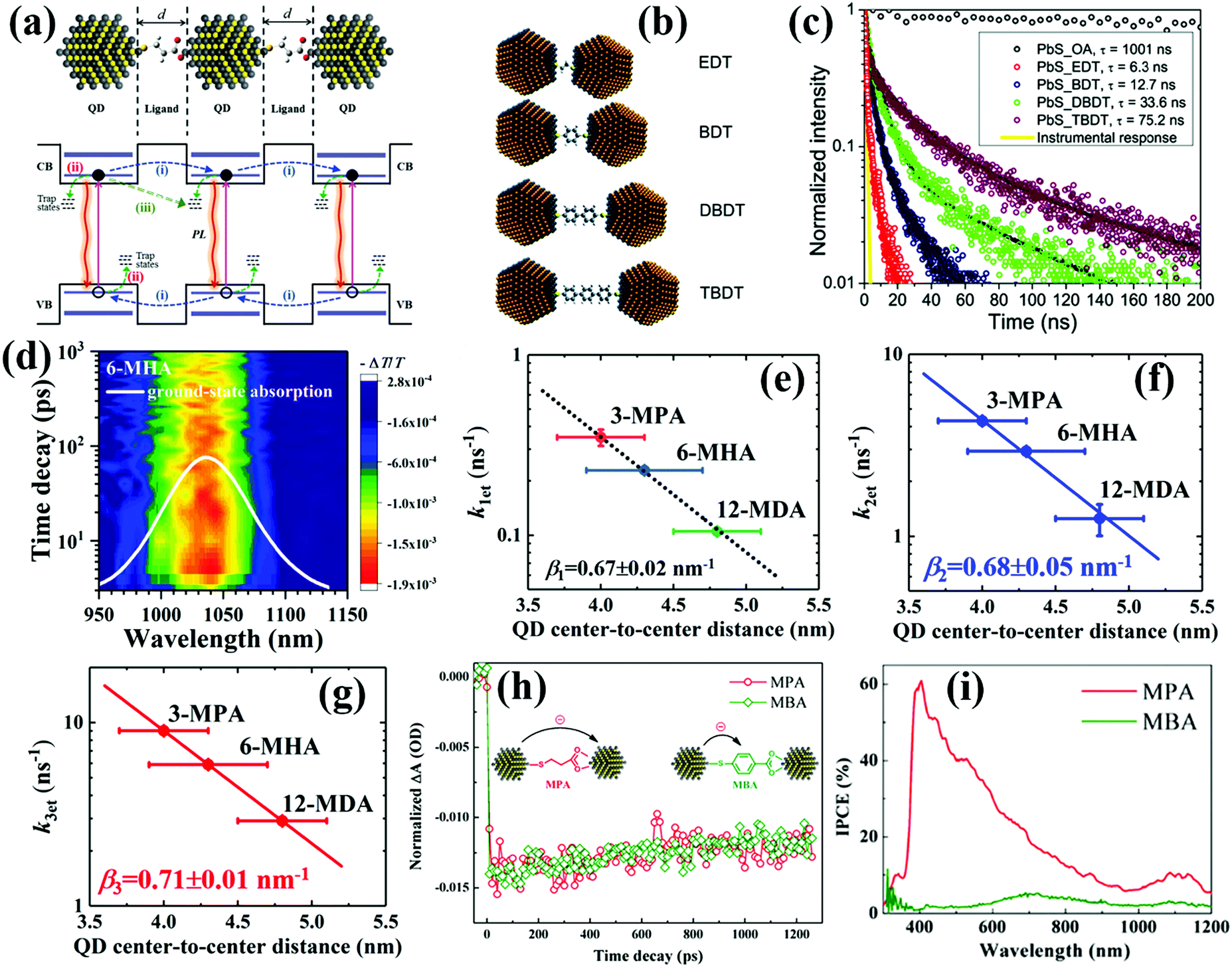 | ||
| Fig. 13 (a) Schematic of the exciton relaxation processes in QD solid films. Including: (i) exciton dissociation (i.e. photoexcited electron and hole transfer) between adjacent QDs; (ii) carrier trapping; (iii) energy transfer between adjacent QDs. (b) Illustration of QDs linked with variable length alkyl and benzene dithiol ligands. (c) TRPL decay curves from the PbS QD assemblies with different ligands show a clear trend of longer PL lifetime with larger interparticle distance. (d) Spectro-temporal TA spectrum of 6-MHA-treated PbS QD solid films. (e–g) Correlation between the averaged QD interparticle distance and the photoexcited exciton dissociation rate constants of the single exciton (k1et), biexciton (k2et) and triexciton (k3et), respectively. (h) TA decay curves of 3-MPA-treated and MBA-treated PbS QD solid films. (i) IPCE spectra of QDSCs based on PbS-MPA and PbS-MBA QD solid films. (a, h and i) Adapted with permission from ref. 191. Copyright (2017) Royal Society of Chemistry. (b and c) Reprinted with permission from ref. 192. Copyright (2010) American Chemical Society. (d–g) Reprinted with permission from ref. 194. Copyright (2019) Royal Society of Chemistry. | ||
4.1 Interparticle distance dependent exciton dissociation in quantum dot solid films
The interparticle distance of adjacent QDs can be regulated by controlling the length of surface ligands. In order to investigate exciton dissociation behavior in the QD solid film, Choi et al. combined time-resolved photoluminescence (TRPL) and time-resolved electric force microscopy (TREFM) to reveal the relationship between interparticle distance and exciton dissociation in PbS QD solid films.192 By using variable length alkyl based dithiol ligands such as 1,2-ethanedithiol (EDT), 1,4-benzenedithiol (BDT), 4,4′-dibenzenedithol (DBDT), and 4,4′′-tribenzenedithiol (TBDT) to precisely control the interparticle distance of PbS QDs (Fig. 13b). It is found that the lifetimes of photogenerated excitons decrease exponentially with the decreasing interparticle distance of PbS QDs and the quenched excitons result in free carriers in the solid films (Fig. 13c). The correlation between interparticle distance and dissociation rate of a single exciton shows a monoexponential decay behavior which indicates that the exciton dissociation in QD solid films occurs via tunneling. Lingley et al. reported that the exciton relaxation pathway in the QD solid film was dependent on the competition of exciton dissociation rate and non-radiative energy transfer rate which was as a function of both temperature and ligand-controlled interparticle distance.193 If energy transfer is forbidden, the TRPL decay shows monoexponential behavior which is consistent with exciton tunneling.By using transient absorption (TA) spectroscopy (Fig. 13d), our group has systematically investigated the interparticle distance related to single and multiple exciton dissociation in QD solid films.148,191,194 We used several mercaptoalkanoic acids (MMAs) with different alkyl chain lengths to adjust the interparticle distance of PbS QD ensembles, such as thioglycolic acid (TGA), 3-MPA, 4-mercaptobenzoic acid (4-MBA), 6-mercaptohexanoic acid (6-MHA), 12-mercaptohexanic acid (12-MDA), 16-mercaptohexadecanoic acid (16-MHDA) and oleic acid (OA). The exciton dissociation rate constants ket of the multiple excitons within the QD solid film similar to that of a single exciton is exponentially enhanced with the decreased QD interparticle distance (d) (Fig. 13e–g), signifying that photoexcited exciton dissociation occurs in the QD solid film via the tunneling effect. The obtained exciton tunneling decay constants (β, the relationship between ket and d is ket ∝ exp(−βd)) for the single exciton, biexciton and triexciton in the PbS solid films are 0.67 ± 0.02 nm−1, 0.68 ± 0.05 nm−1 and 0.71 ± 0.01 nm−1, respectively.194 In addition, we also investigated the ligand scaffold effects on the exciton dissociation and the performance of the corresponding QDSCs.191 We select the conjugated molecule (MBA) which contains a benzene unit and non-conjugated molecule MPA as the capping ligand for the PbS QD solid film and QDSCs. The TA decay curves of PbS-MPA and PbS-MBA QD solid films indicate that the exciton dissociation rate in both films is nearly the same (Fig. 13h), but the monochromatic incident photon to current conversion efficiency (IPCE) value of the PbS-MBA based QDSCs is dramatically lower than that of PbS-MPA based ones (Fig. 13i), which is caused by the lower charge collection efficiency in a PbS-MBA based device. This result is attributed to the charge transfer from PbS QDs to MBA rather than adjacent QDs. We also compared the exciton dissociation behavior in PbSe QD solid films treated with short organic ligands (EDT and MPA) and organic halide salts (CTAB and TBAI).148 Halide anion (Br− and I−) treated PbSe QD solid films exhibit faster exciton dissociation rate and lower trap-state density than organic ligand treated films.
Kanemitsu and coworkers investigated the importance of interparticle distance on the MEG property and the photoexcited exciton dissociation in QD solid film by using various organic and inorganic ligands.75 The optical and electrical properties of those PbS QD solid films are determined by the interparticle spacing between QDs (Fig. 14a). The PL peak energy of different ligand treated QD solid films is redshifted by decreasing the QD interparticle distance which is caused by the enhanced electronic interactions between QDs, while the intensity of the PL is reducing which is caused by the exciton dissociation in the QD solid film. The dark conductivities in those QD solid films change exponentially with interparticle distance (Fig. 14a), which indicates that exciton dissociation in the film is dominated by charge tunneling between the neighboring QDs. The impact of interparticle distance on the MEG property in the QD solid film was also investigated. After analyzing the photocurrent enhancement data of the QD solid film treated with different ligands under weak excitation energy (Fig. 14b), the evaluated MEG efficiencies (ηMEG) for KSCN-treated, 2-aminoethanol (AE)-treated, and EDT-treated QD solid films are 0.792(±0.017), 0.691(±0.020) and 0.721(±0.020), respectively. The corresponding MEG threshold (hνMEG) for those films is 2.26(±0.03) Eg, 2.45(±0.04) Eg and 2.39(±0.04) Eg, respectively. This result indicates that MEG is more likely to occur in KSCN-treated PbS QD solid films due to the much shorter interparticle distance in KSCN-treated film than the other two films (Fig. 14a). After that, the Kanemitsu group further investigated the exciton dissociation in PbS QD solid films treated with short ligands using TA spectroscopy (Fig. 14c).195 Similar to the case of single excitons, the decay rates of multiple excitons between adjacent QDs increase with the photoconductivity of PbS QD solid films (Fig. 14d), and the exciton dissociation process determines the photocurrent of QDSCs due to MEG. The photoexcited exciton dissociation rate between QDs dependent on the QD interparticle distance, which in turn affects the performance of the QDSC device. Shorter interparticle distance results in the increase of the wave function overlap of adjacent QDs. Therefore, QD solid films treated with small and stable ligands are expected for promising QDSCs with high efficiency and stability.
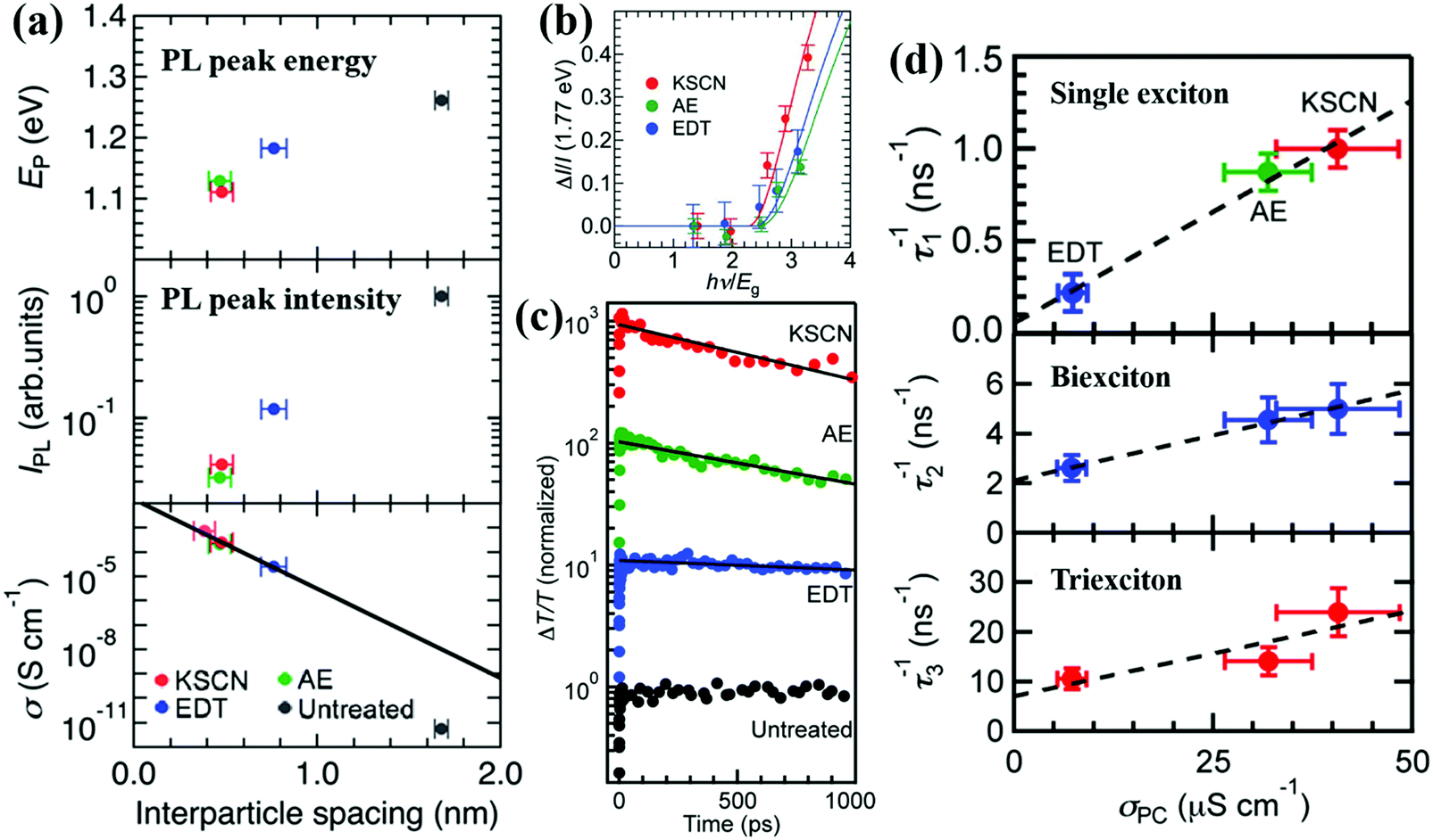 | ||
| Fig. 14 (a) PL peak energy, PL peak intensity, and dark conductivities of different ligand treated PbS QD solid films as a function of the interparticle spacing between QDs. (b) Plots of normalized photocurrent enhancements for different ligand treated QD solid films, ΔI/I(1.77 eV), against the excitation energy (hν) divided by the optical band gap (Eg). (c) Exciton relaxation dynamics for the PbS QD solid films treated with different ligands measured using TA spectroscopy. The solid curves are the fitting curves. (d) Correlation between the photoconductivity of PbS QD solid film treated with different ligands and the decay rates of single excitons, biexcitons and triexcitons in those films. (a and b) Reprinted with permission from ref. 75. Copyright (2014) Royal Society of Chemistry. (c and d) Reprinted with permission from ref. 195. Copyright (2015) American Chemical Society. | ||
4.2 Carrier recombination in quantum dot solid films and halide ion passivation
The interparticle distance affects the exciton dissociation behavior in QD solid films and the shorter interparticle distance results in a faster exciton dissociation rate. After exciton dissociation (electron and hole separation), carriers (both electron and hole) can freely transport in QD solid films. To obtain high conductivity QD solid films, the electrically insulating original ligand of the QD, such as OA, OLA or TOP etc., must be removed from the surface of the QD. Short ligands such as metal chalcogenide complexes (MCCs), MPA, EDT and BDT are usually used to replace the original ligand of the QD.19,196–201 However, due to the poor passivation of these ligands, serious surface and interfacial carrier recombination caused by trap-states exists in these QD solid films. As we mentioned in Section 3.3, halide can effectively reduce the surface defect of colloidal QDs, and halide anion treatment allows fast carrier transfer between adjacent QDs (tens or hundreds of ps), while the strong binding of halides to surface metal atoms of QDs offers the capacity to improve the stability of the QD solid film.19 Halide ligands have been widely used for deposition of QD active layers of QDSCs since they were first reported by Tang et al.169 Compared with bromide and chloride ligands, iodide ligands are difficult to be removed from the QD's surface by protic solvent due to forming stronger bonds to surface metal atoms of the QD, in turn bringing much lower film trap-state density.148,202,203 This phenomenon can be explained by hard-soft-acid–base (HSAB) theory that the iodide as a soft base can be bound strongly with lead atoms as a soft acid on PbS QDs.203–205In QDSCs, the presence of sub-bandgap states in the QD active layer results in large VOC deficit and poor carrier collection.206,207 Surface hydroxyl (OH) is considered to be the main cause of sub-bandgap trap-states and is difficult to remove completely during the solid-state ligand-exchanging process, in turn preventing complete passivation with iodide ligands.176,208,209 Thus changing the surface passivation process, especially eliminating the surface OH which is beneficial for stabilizing QDs,210 has a great potential to reduce the surface trap-state density and improve the photovoltaic performance of QDSCs. Cao et al. reported that a mild thermal annealing (at 80 °C in an inert atmosphere for 10 min) process was advantageous to reducing the weight of Pb-OH and further improving the iodide surface passivation of PbS QDs (Fig. 15a and b).208 An imidazolium iodide salt named 1-ethyl-3-methylimidazolium iodide (EMII) is introduced as an iodide ligand source in PbS QDSCs which has a cation with a delocalized positive charge and a less steric planar structure compared to TBAI (Fig. 15d). Compared with the TBAI-treated PbS QD solid film, hydroxide species are reduced and iodide passivation is improved in EMII treated films (Fig. 15c). Another imidazolium iodide salt named 1-propyl-2,3-dimethylimidazolium iodide (PDMII) was also used as an iodide ligand source to reduce the surface trap-state density on the PbS QDs.171 It is found that both oleate-ligand and OH groups are effectively removed from the QD's surface after PDMII treatment. Compared with TBAI, the improved surface passivation by PDMII effectively reduced the sub-bandgap states which is confirmed by the PL emission quenching at 1300–1600 nm (Fig. 15e). After PDMII treatment, the free carrier lifetime of the QDSCs is increased from 5.5 μs to 7.4 μs which is obtained from the transient photovoltage (TPV) decay measurement (Fig. 15f). This result leads to enhanced carrier extraction properties and reduced VOC deficit in the QDSC device. We would like to remind the reader here that, unlike the exciton lifetime (obtaining from TA measurement) or PL lifetime (obtaining from TRPL measurement) in a single QD which is mentioned earlier in this review, the TPV decay measurement is used to obtain the free carrier lifetime in the entire QDSC device under open circuit conditions.
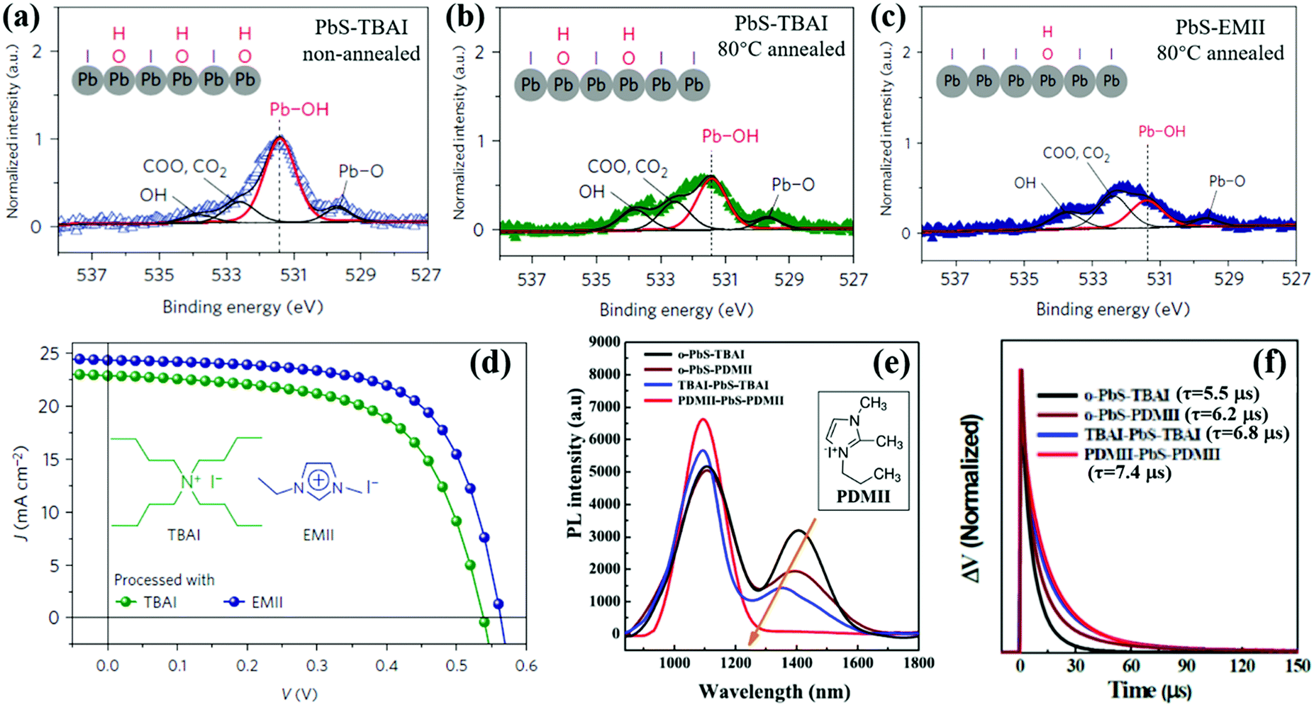 | ||
| Fig. 15 (a) X-ray photoelectron spectroscopy (XPS) signal from O 1s of the non-annealed PbS QD layer processed with TBAI. (b) XPS signal from O 1s of the 80 °C-annealed PbS QDs layer processed with TBAI. (c) XPS signal from O 1s of the 80 °C-annealed PbS QDs layer processed with EMII. (d) Current density–voltage (J–V) curves of 80 °C-annealed QDSCs processed with TBAI and EMII. (e) PL spectra of four PbS QD solid films with different treatments. The peak at ∼1100 nm belongs to band-edge emission and the weak peak at 1300–1600 nm belongs to sub-bandgap emission. (f) The TPV spectroscopy of four types of devices with different surface treatment. (a–d) Adapted with permission from ref. 208. Copyright (2016) Spring Nature. (e and f) Adapted with permission from ref. 171. Copyright (2017) Elsevier. | ||
Similar to organic ones, inorganic halide salts can be also widely used as a halide ligand source to reduce the trap-state density in QD solid films. Dirin et al. introduced various metal halide complexes as inorganic capping ligands for QDs and obtained stable fully halide-covered QD colloidal solutions (Fig. 16a).211 The Lewis acid–base properties and dielectric constant of the solvents must be properly adjusted for successful ligand exchange and colloidal stability. Luther et al. firstly used metal halide salts as ligands to deposit the QD active layer of PbS and PbSe QDSCs.184 PbI2-Treated QD solid film exhibits a deeper work function and energy level positions than other reported ligands (Fig. 16b). Due to the increased thickness and improved carrier transport of the QD active layer, PbS QDSCs reached a PCE of 7.25%. The post-film processing metal halide treatment can also efficiently improve the VOC and air stability of the PbSe QDSCs.212 Ammonium iodide (NH4I) is also employed as an iodide source to passivate QDs that is stabilized in polar solution without particle aggregation.213–215 By using PbS-NH4I/N,N-dimethylformamide (DMF) solution as QD ink, the active layer of the PbS PDHJ-QDSCs is deposited by a one-step deposition process.213 To form a thick one-step QD solid film from the QD ink, the QDs must be dispersed in a fast-drying solvent with high concentrations and the residues which inhibit carrier transfer in the QD solid film must be completely removed from the inks. The Sargent group developed a novel lead halide (PbX2)/ammonium acetate (AA)/DMF solution-state ligand exchange method then deposited a QD solid film in a one-step strategy by using the resulting QD ink.216–218 Compared with the QD solid films fabricated by organic iodide salt (TBAI) and conventional solution exchange methods, the QD solid film deposited using new QD ink exhibits a sharper bandtail and reduced energy funneling (Fig. 16c and d) which effectively decreases the sub-bandgap states and improves the carrier transfer.216 After optimization, a certified record efficiency of 12% was obtained.218 Synergistic hybrid ligand treatment was recently proposed to reduce the sub-bandgap states in QD solid film and the VOC deficit of devices.219,220 In the ZnI2/MPA mixed-ligand system, the ZnI2 ligand works as an iodide ligand to obtain a better carrier transport QD solid film, while an MPA ligand can simultaneously suppress the generation of sub-bandgap states and improve the surface protection of QDs. This synergistic hybrid ligand treatment strategy leads to a low VOC deficit of 0.4 V for PbS QDs in BDHJ-QDSCs.220
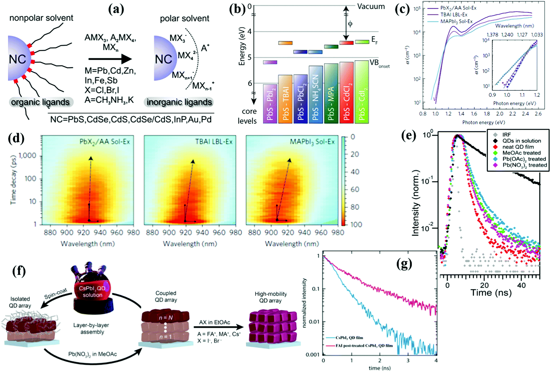 | ||
| Fig. 16 (a) Schematics of the ligand exchange methodology for obtaining metal halide capped colloidal QDs. (b) Energy level diagrams of PbS QD (1.3 eV) solid films treated with various ligands. (c) Photothermal deflection spectroscopy measurements for three PbS QD solid films. The calculated Urbach energies for the PbX2/AA-exchanged, TBAI-exchanged, and MAPbI3-exchanged film are 29 meV, 33 meV and 44 meV, respectively. (d) Spectro-temporal TA maps for PbX2/AA-exchanged, TBAI-exchanged, and MAPbI3-exchanged QD solid films. A contour filter was applied to improve the signal-to-noise ratio. The peak position redshift of the transient bleach spectra correlates with the degree of energy disorder with energy funneling towards undesired bandtail states. (e) TRPL decay plots of CsPbI3 QDs in solution compared to films of these QDs under various ligand treatments. (f) Schematic of the CsPbI3 QD solid film deposition process and AX salt post-treatment. (g) TRPL decay plots for CsPbI3 QD solid films with (pink) and without (blue) FAI post-treatment. (a) Reprinted with permission from ref. 211. Copyright (2014) American Chemical Society. (b) Reprinted with permission from ref. 184. Copyright (2015) Springer Nature. (c and d) Reprinted with permission from ref. 216. Copyright (2016) Springer Nature. (e) Reprinted with permission from ref. 221. Copyright (2016) AAA Science. (f and g) Reprinted with permission from ref. 223. Copyright (2017) AAA Science. | ||
Recently, an anti-solvent washing approach can efficiently remove electrically insulating original ligands of perovskite QDs. Since perovskite QDs are very sensitive to polar solution and tend to react with halide ions through anion-exchange reaction, it's not feasible to fabricate perovskite QDSCs using a similar method as lead chalcogenide QDSCs. The Luther group creatively used methyl acetate (MeOAc) as an anti-solvent to purify perovskite QDs.221,222 A small amount of Pb(OAc)2 in MeOAc can improve the surface passivation of α-CsPbI3 QDs, which results in enhancement of the PL intensity and longer TRPL lifetime compared with using MeOAc alone (Fig. 16e). The films obtained via this method exhibit small VOC deficit and the resulting QDSCs achieve PCEs up to 10.77%. A further improved PCE based on perovskite QDSCs of 13.43% is achieved by tuning the surface chemistry of CsPbI3 QDs based on A-site cation halide salt treatments (Fig. 16f).223 This post-film passivation method results in enhanced QD coupling, improved mobility and increased carrier lifetime (Fig. 16g), which indicates that this strategy is of great value to improve the charge-carrier transport properties of perovskite QD solid films.224 The Liu group recently confirmed that the post-film passivation strategy by formamidinium iodide (FAI) could improve charge transport of CsPbI3 QD solid film as reported by the Luther group.225 Although the certified record PCE of perovskite QDSCs has reached 16.6%,18 the poor environmental stability and photostability under continuous illumination of perovskite QDs set a barrier to improve the performance of QDSCs. Novel ligands and careful surface passivation of perovskite QDs are therefore needed to further improve their stability.
As discussed in this section, the interparticle distance and sub-bandgap states in QD solid film can be well controlled by the surface ligand of the QDs, thus affecting the photoexcited carrier transfer and recombination dynamics in the QD solid film. Although the photovoltaic performance of QDSCs has sharply increased in recent years via ligand engineering, the PCE of QDSCs is still below its theoretical value and the device stability also needs to be further improved. Novel ligands, efficient ligand exchange methodology and QD solid film deposition technology are therefore required to improve carrier transfer and reduce sub-bandgap states along with enhancing the stability of the QD solid film.
5. Photoexcited carrier dynamics at the interfaces of the QDSCs
In DHJ-QDSCs, after the photoexcited carriers undergo picosecond cooling, they transport through the QD solid film and then reach the electron transport layer (ETL)/QDs and QDs/metal electrode interfaces, respectively. Both electrons and holes have to be efficiently collected from the QD solid film by the ETL and metal electrode before direct recombination, respectively. The collected electrons and holes are still easily recombined with interfacial defects or the residual charges in the QDs through a slow interfacial recombination process (Fig. 17a). Different from DHJ-QDSCs, for sensitized-QDSCs, although the photoexcited carriers can directly transfer from the QDs into the ETL which has the potential to obtain larger charge collection efficiency than DHJ-QDSCs, the electrolyte in the device will capture those carriers and cause photocorrosion of the QDs which greatly enhances carrier recombination as well as reduces carrier collection and stability of the devices (Fig. 1d). Thus, improving carrier extraction or collection at those interfaces and suppressing interfacial recombination are necessary requirements for obtaining high performance QDSCs. The fast carrier extraction or injection process at the ETL/QDs interface can be observed by ps-transient absorption (TA) spectroscopy, transient terahertz (THz) spectroscopy or time-resolved photoluminescence (TRPL) spectroscopy, and the slow interfacial carrier recombination can be detected by ns-TA spectroscopy,226–231 transient photovoltage (TPV) decay measurement,228,232–235 and impedance spectroscopy.236–242 Understanding carrier dynamics at each interface, improving carrier collection and reducing carrier interfacial recombination are important avenues to enhance the photovoltaic performance of QDSCs. | ||
| Fig. 17 (a) Schematic of the photoexcited carrier injection and recombination processes in QDSCs. (b) Schematic band diagram of the PDHJ-QDSCs with Sb-doped, Zr-doped and undoped anatase TiO2 at equilibrium. (c) The external quantum efficiency (EQE) spectra of QDSCs based on undoped, Sb-doped and Zr-doped TiO2 as an ETL in QDSCs. (d) The built-in voltage potential at the In:ZnO/QD interface as a function of In3+ doping concentration. (e) Energy diagram of different sizes of CdSe QDs and metal oxide semiconductors. (f) QD size-dependent ΔG and electron transfer rate constant ket at the ETL/CdSe QD interface. (g) The size-dependent electron transfer behavior monitored by ps-THz spectroscopy on PbSe QD sensitized SnO2 films. (b and c) Reprinted with permission from ref. 247. Copyright (2011) Wiley. (d) Reprinted with permission from ref. 248. Copyright (2016) Wiley. (e and f) Reprinted with permission from ref. 244. Copyright (2011) National Academy of Sciences. (g) Adapted with permission from ref. 251. Copyright (2011) American Chemical Society. | ||
5.1 Electron transfer at the electron transport layer/quantum dot interface
Until now, the extraction of hot electrons in QDSCs is still not implemented due to the fast cooling rate of hot excitons in QDs as we mentioned above. Thus, the study on the cold electron and hole dynamics in QDSCs is of great significance. The cold electron transfers into the ETL through the ETL/QDs interface with a required high electron transfer rate to avoid carrier accumulation and recombination in the QDs. The cold electron transferred from the QD to the ETL has been successfully evaluated in terms of Marcus theory.243–245 The functional form of the Marcus model is described as follows: | (5) |
 | (6) |
Wide bandgap metal oxide semiconductors such as TiO2, ZnO and SnO2 are commonly employed as the ETL in QDSCs. Metal cation doping is the most effective way to adjust the property of these materials, such as band level, carrier mobility and deep trap-state density. Several metals such as Al, Cu, Nb, W and Cr have been reported to adjust the intrinsic conductivity of the metal oxides.246 Liu et al. systematically investigated the incorporation of various metal ions to tune the properties of TiO2.247 After Sb-doping or Zr-doping, the band structure of TiO2 matches well with the CB position of PbS QDs (Fig. 17b). This results in improved electron collection efficiency at the TiO2/PbS QD interfaces, which is confirmed by IPCE spectra of these devices (Fig. 17c). Iodide-treated PbS QDs exhibit n-type behavior (which can be confirmed by the corresponding FET device) (Fig. 12b) and consequently very little band bending at the ETL/QDs junction emerges along with reducing the electron collection at this interface. Thus, building a much stronger n +/n junction at the ETL/QD interface is required. Liu et al. achieved this by doping In3+ into ZnO nanoparticles. The band structure and carrier concentration of ZnO can be simultaneously adjusted by controlling the doping amount of In3+.248 After doping, the carrier concentration of ZnO was increased up to 5 × 1019 cm−3, and a significant built-in electric field at the ZnO/QDs interface considerably improves the electron collection efficiency (Fig. 17d). Cs+ doping can also effectively adjust the band structure and reduce the trap-state density of ZnO, which exhibits significantly improved electron collection at the ETL/QD interface.249,250
According to eqn (5) and (6), the size of the QD plays a critical role to affect the value of ΔG and finally affect the electron transfer rate and injection efficiency at the ETL/QDs interface.252–254 Tvrdy et al. employed a series of different size CdSe QDs to investigate the electron transfer behavior between CdSe QDs and metal oxide semiconductors.244 As the CB position of the QD can be adjusted by changing its size, the bigger ΔG between the ETL/QDs is obtained when using smaller size CdSe QDs (Fig. 17e). Smaller size CdSe QDs with a bigger ΔG exhibit a faster electron transfer at the ETL/QD interface than that of larger size CdSe QDs (Fig. 17f). A similar result was found in the SnO2/PbSe QDs sensitized system reported by Cánovas et al.251 The size-dependent electron transfer process from the PbSe QD to SnO2 was recorded by ps-THz spectroscopy (Fig. 17g). The value of ket is increased from 1.44 × 10⁹ s−1 for 7.76 nm PbSe QDs to 8.33 × 10⁹ s−1 for 2.15 nm PbSe QDs with the value of ΔG increased from 0.33 eV to 0.74 eV, respectively. In our recent work, the QD size-dependent electron transfer from CsPbI3 QDs to ETLs was also monitored by ps-TA spectroscopy (Fig. 18a–d).245 The ket values of electron transfer from CsPbI3 QDs to TiO2 are 2.10 × 10¹⁰ s−1, 1.76 × 10¹⁰ s−1, and 1.30 × 10¹⁰ s−1 for 10 nm, 12 nm, and 15 nm diameter QDs, respectively. Notably, the electron injection efficiency in the TiO2/CsPbI3 QD system can reach as high as 99% for all sizes of CsPbI3 QDs. In addition, the electron transfer behavior from CsPbI3 QDs (12 nm) to ZnO is also measured. Although the ΔG in the ZnO/QDs system is slightly smaller than that in the TiO2/QDs system (Fig. 18e), the electron transfer process with a smaller ket of 0.70 × 10¹⁰ s−1 is much slower than that in the case of TiO2 in the ZnO/QDs system (Fig. 18f). According to Marcus theory, the large differences of electron transfer dynamics between the TiO2/QDs and ZnO/QDs system are mainly attributed to the distinctions of both the coupling degree effect and electron accepting-state density in different metal oxide semiconductors.245
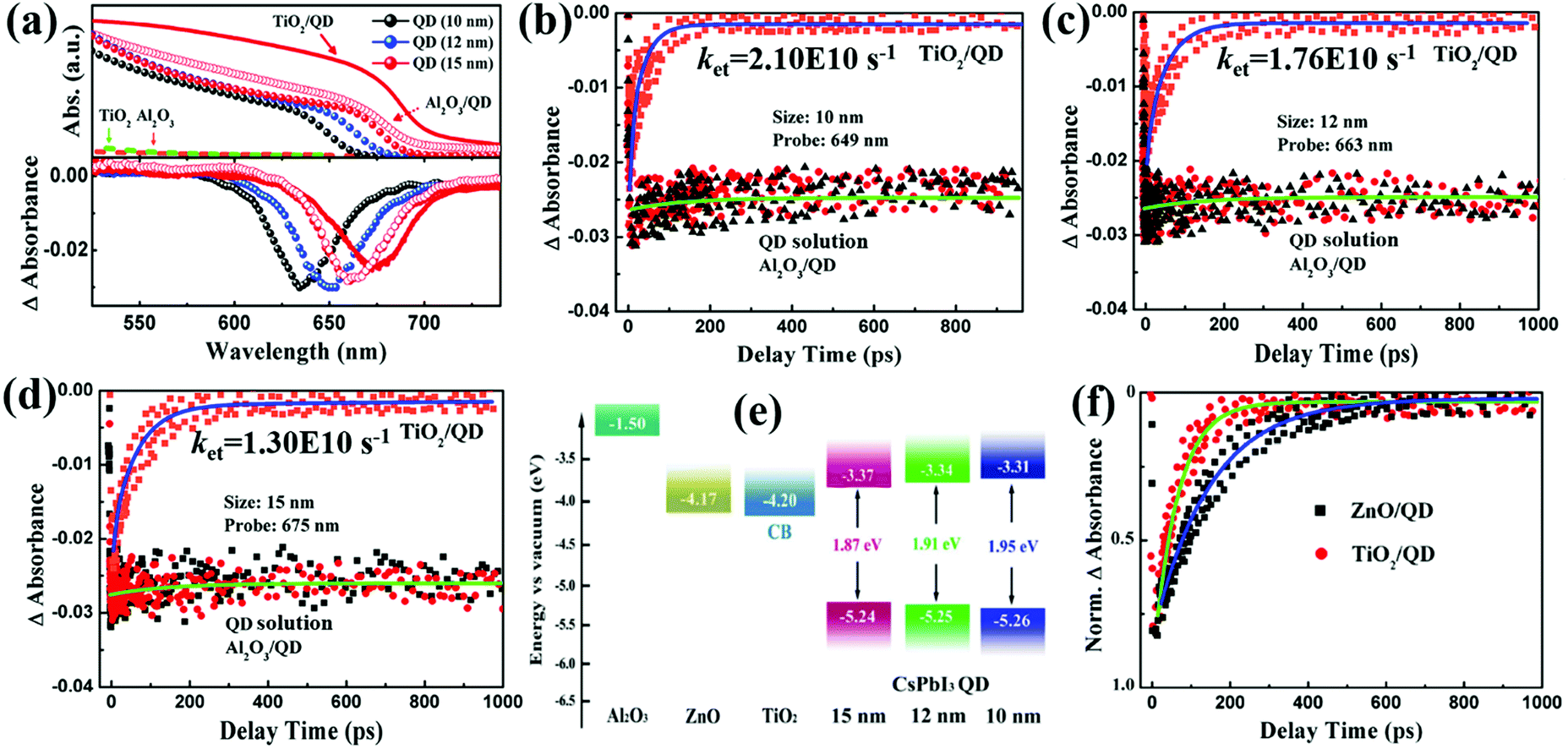 | ||
| Fig. 18 (a) Absorption (top half) and TA spectra (bottom half) of a series of CsPbI3 QDs in hexane, TiO2/CsPbI3 QD (15 nm) and Al2O3/CsPbI3 QD (15 nm) films. (b–d) TA bleaching decay of different-sized QDs in hexane and absorbed to TiO2 and Al2O3. The solid line is the exponential fitting curves from the TA dynamics. (e) Energy level diagrams of the metal oxide semiconductors and difference sizes CsPbI3 QDs. (f) Comparison of the TA bleaching decay of 12 nm CsPbI3 QDs attached to TiO2 and ZnO. Reprinted with permission from ref. 245. Copyright (2018) American Chemical Society. | ||
It has been confirmed that reducing the ETL–QD separation distance is beneficial for improving electron transfer at the ETL/QDs interface especially for sensitized QDSCs.255–257 In sensitized QDSCs, the high-quality pre-synthesized QD is absorbed on metal oxide semiconductor electrodes by the use of linker molecules, and thus the electron transfer dynamics at the ETL/QDs interface can be controlled by the functional group and length of linker molecules.255 Yang et al. reported that the JSC values of both CdSe and CdSexTe1−x sensitized QDSCs with the use of the TGA linker were higher (8–13% increased) than those of 3-MPA and cysteine based devices.258 This is ascribed to the reduced ETL–QD separation distance, which leads to the observed increase of electron transfer rate at the TiO2/CdSe QD interface (Fig. 19a). Hines et al. revealed that the electron transfer dynamics at the ETL/QDs interface was dependent on the functional group of the linker molecule.259 Compared with 3-MPA, the electron donating amine group of β-alanine can reduce the intrinsic surface trap-states of CdSe QDs, which can facilitate the electron transfer process and result in about 3 times larger electron transfer rate at the ETL/QDs interface. Ligand type affects the strength of coupling and results in different electron transfer dynamics at ETL/QDs interface and photovoltaic performance of QDSCs.260 Compared with short organic ligands, the electron transfer rate of atomic S2−-capped CdSe QDs at the ETL/QDs interface is much larger due to the enhanced electron coupling and results in a higher external quantum efficiency (EQE) (Fig. 19b and c).261,262 Besides atomic S2−, metal chalcogenide surface ligands can also be used to facilitate the electron transfer process in sensitized QDSCs.263 As we mentioned in Section 4 (Fig. 12a), surface ligands can affect the energy level of QDs. Thus, surface ligands or linker molecules have a great influence on the electron transfer dynamics at the ETL/QDs interface. In addition, for core/shell structure QDs, although the shell layer can efficiently reduce the surface trap-state density and improve the stability of the core, the shell layer usually acts as a barrier layer for electron injection from QDs to the metal oxide semiconductor electrode leading to a reduced electron transfer rate constant (ket) (Fig. 10a–c). Thus, it is required to balance the competitive effect between the reduced trap-state density and the enhanced electron transfer rate for improving the photovoltaic performance of the QDSCs.
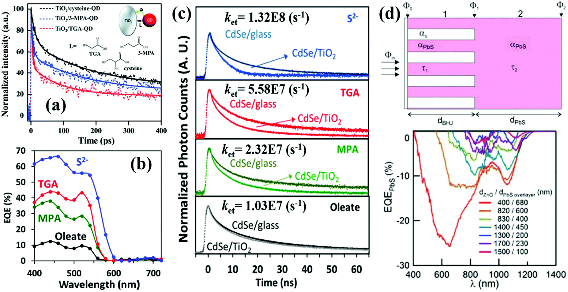 | ||
| Fig. 19 (a) TG responses of TGA-, MPA- and cysteine-capped CdSe QDs deposited on TiO2 nanoparticle substrates. (b) The EQE spectra of oleate-, MPA-, TGA-, and S2−-capped CdSe QD sensitized QDSCs. (c) The TRPL decay curves and the calculated electron transfer rate constants (ket) of oleate-, MPA-, TGA-, and S2−-capped CdSe QDs on glass and TiO2. (d) Upper: The scheme of carrier transport theoretical model in BDHJ structure QDSCs. Bottom: The EQE spectra of PbS BDHJ structure QDSCs with different ZnO nanowires (NWs) lengths and QDs overlayer thickness. (a) Adapted with permission from ref. 258. Copyright (2014) Royal Society of Chemistry. (b and c) Reprinted with permission from ref. 261. Copyright (2014) American Chemical Society. (d) Adapted with permission from ref. 273. Copyright (2015) American Chemical Society. | ||
In depleted-heterojunction (DHJ)-QDSCs, a depletion region can be formed near the ETL/QD interface with a great influence on the photoexcited exciton separation and electron extraction.197,264 To absorb all incident light, it is better to fabricate the thickness of the QDs active layer as about 1 μm.265 Generally in planar depleted-heterojunction (PDHJ)-QDSCs, the efficient carrier extraction can only be achieved for about a 300 nm thick QD layer which includes less than 100 nm minority carrier diffusion length and 200 nm thick depletion region.199,265,266 Bulk depleted-heterojunction (BDHJ) architecture is an effective design to extend the depletion region and increase the thickness of the QD active layer,220,267–269 which can improve both optical absorption and charge collection efficiency (Fig. 1c and 19d). The shortened electron transport length to an ETL electrode is advantageous to reducing the carrier recombination probability during a carrier transport process. Thus, aiming at realizing a BDHJ structure QDSC, various one-dimensional (1D) TiO2 and ZnO materials, such as nanorods (NRs) and NWs, have been explored as the ETL in QDSCs.162,265,269–272
5.2 Carrier recombination at the electron transport layer/QDs interface and solution strategy
In QDSCs, interfacial carrier recombination usually occurs across the electron transport layer (ETL)/QDs interface with the accepted electrons in the CB of the metal oxide semiconductor recombining with the remaining holes in the VB of the QDs (Fig. 17a). This interfacial carrier recombination pathway is one of the main causes of the larger VOC deficit and JSC reduction. Kemp et al. described the interfacial carrier recombination at the ETL/QD interface using a modified Shockley–Read–Hall model.274 The interfacial carrier recombination rate is established by the following equation: | (7) |
Compared with TiO2, ZnO has been widely used as an ETL in solid-state QDSCs because of its higher electron mobility (130–200 cm2 V−1 s−1) and suitable conduction band edge that are favorable for electron transport with less recombination and obtaining a larger VOC.162,218,275 However, the deep-level trap-states caused by oxygen vacancies and interstitial zinc,276,277 along with the surface trap-states which are contributed by the surface absorbed oxygen and hydroxyl groups,278 buildup multiple carrier recombination centers in the bulk and surface of ZnO. Annealing, doping and surface passivation by small molecules have been reported to reduce the trap-state density in ZnO.24,277,279–285 For instance, Azmi et al. used 1,2-ethanedithiol (EDT) molecules to modify the ZnO surface to effectively reduce the trap-state density of the ZnO by passivation of the oxygen-deficient defects, elongate larger free carrier lifetime, suppress the interfacial carrier recombination, and improve the interfacial carrier extraction at the ZnO/PbS QDs heterojunction (Fig. 20a and b).286 By using this EDT modified ZnO electrode, a certified PCE of 10.14% for PbS QDSCs is achieved. In our recent work, Mg-doped ZnO (Zn1−xMgxO) was used as an ETL in PbS QDSCs.276 Low molar Mg-doping can reduce both the shallow trap-state and deep-level trap-state of ZnO (Fig. 20c). By changing the doping amount of Mg2+, the band structure, trap-state distribution and carrier concentration of Zn1−xMgxO can be well adjusted. We used ps-TA spectroscopy to reveal the role of Mg-doping in the photoexcited carrier dynamics at the ETL/PbS QD (1.19 eV) interface. If an electron is injected from the PbS QD to the Zn1−xMgxO electrode, positive TA response can be found from TA spectroscopy in the infrared range (over 1400 nm) which belongs to the absorption of the free electrons in the ETL. We investigated the electron injection and carrier recombination at the Zn1−xMgxO/PbS QD interface by analyzing the dynamics of free electrons in Zn1−xMgxO (TA probe wavelength is 1500 nm). A similar TA signal growth process (electron injection process) for ZnO/PbS QD and Zn0.9Mg0.1O/PbS QD samples is obtained, indicating that low molar Mg-doping does not hinder the injection of electrons from PbS QDs to Zn1−xMgxO. Subsequently, a much slower TA signal decay process (interfacial carrier recombination process) can be observed for Zn0.9Mg0.1O/PbS QD sample (Fig. 20d). A similar trend is monitored in the transient photovoltage (TPV) decay measurement of QDSCs (Fig. 20e). These results indicate that low molar Mg-doping in ZnO is conducive to reducing carrier recombination at the ZnO/PbS QDs interface and the VOC deficit of the QDSCs device.
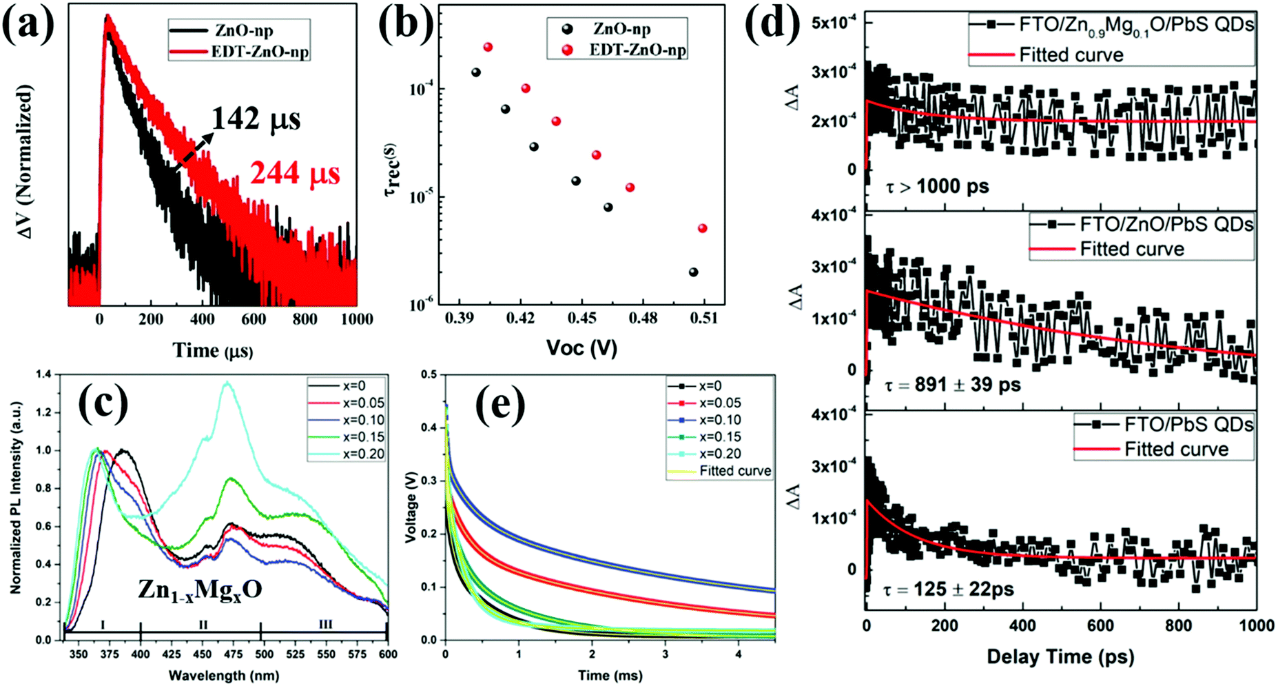 | ||
| Fig. 20 (a) Transient photovoltage decay curves of ZnO based QDSCs with and without EDT passivation. (b) Free carrier lifetime in ZnO based QDSCs with and without EDT passivation. (c) Steady-state PL spectra of Zn1−xMgxO films (x = 0, 0.05, 0.10, 0.15 and 0.20). (d) The TA signal decay curves of the FTO/PbS QDs, FTO/ZnO/PbS QDs, and FTO/Zn0.9Mg0.1O/PbS QDs samples, measured with a pump wavelength of 470 nm and a probe wavelength of 1500 nm. The decay curves can be well fitted by using a monoexponential decay function. (e) The TPV decay curves of Zn1−xMgxO-based QDSCs. (a and b) Reprinted with permission from ref. 286. Copyright (2016) American Chemical Society. (c–e) Reprinted with permission from ref. 276. Copyright (2018) Royal Society of Chemistry. | ||
Introducing a wide bandgap semiconductor as a blocking or passivation layer between the electron transport layer (ETL)/QDs interface is another efficient way to suppress the interfacial carrier recombination in the QDSCs. With the aim to reduce this recombination and to enhance carrier extraction, several semiconductors have been exploited such as amorphous TiO2,232,287 Al2O3,288 SnO2,278 MgO,289 MgZnO,290 and ZnS.291 In our recent work, a thin amorphous TiO2 layer and SnO2 layer are used as a passivation layer to reduce the surface trap-state density on ZnO nanowires (NWs).232,278 The longer free carrier lifetime and larger recombination resistance of the passivated QDSCs indicate that the interfacial carrier recombination at the ETL/QDs is suppressed (Fig. 21a–c). Therefore, the power conversion efficiency (PCE) and stability of QDSCs are significantly improved. Lian and co-worker inserted different thicknesses of Al2O3 insulating layer at the TiO2/PbS QDs interface to ameliorate the electron transfer rates and interfacial carrier recombination.292 The estimated electron transfer time and carrier recombination half-life time by using TA spectroscopy at the TiO2/PbS QD interface are 6.4 fs and 32 ps, respectively, which can be increased to 19 fs and 93 ps by introducing one cycle Al2O3 insulating layer, and then increased to 61 ps and over 1 ns by depositing 3 cycles Al2O3, respectively. Thus, in order to obtain more efficient QDSCs, it is necessary to balance the competitive effect between the reduced interfacial carrier recombination and the enhanced carrier injection in the QDSC device.
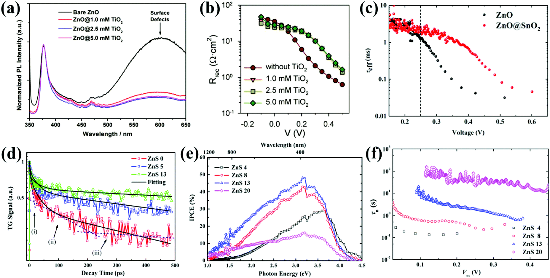 | ||
| Fig. 21 (a) Room temperature PL spectra of bare ZnO NWs and the ZnO NWs treated with the TiO2 precursors of different concentrations (1.0, 2.5 and 5.0 mM). (b) Recombination resistance extracted from impedance spectroscopy of ZnO NWs based QDSCs with and without TiO2 passivation. (c) Free carrier lifetime in ZnO NWs based QDSCs with and without SnO2 passivation. (d) TG responses of TiO2/PbS QDs electrodes with and without ZnS coating. The first two decay processes (i and ii) are assigned to the electron and hole trapping processes, while the third decay process corresponds to the electron injection from PbS QDs to the TiO2 electrode. (e) IPCE spectra of QDSCs with various ZnS coating cycles on TiO2/PbS electrodes. Higher IPCE indicates the larger electron collection efficiency in ZnS coated QDSCs. (f) Calculated free carrier lifetime from transient photovoltage decay curves of QDSCs with various ZnS-coating cycles. (a and b) Reprinted with permission from ref. 232. Copyright (2015) Royal Society of Chemistry. (c) Reprinted with permission from ref. 278. Copyright (2019) Frontiers. (d–f) Reprinted with permission from ref. 293. Copyright (2015) Elsevier. | ||
5.3 Carrier recombination at photoanode/electrolyte interface and solution strategy
In sensitized QDSCs, the ETL and QDs directly contact with the electrolyte, thus electrons in both the ETL and QDs can be easily captured by the redox couple in the electrolyte. Introducing a passivation layer to prevent direct contact of ETL/QDs (photoanode) and electrolyte is proved to be an efficient way to reduce carrier recombination at the photoanode/electrolyte interface, and further to achieve a high PCE of QDSCs.162,294 A thin ZnS layer was firstly used by Yang et al. to coat the TiO2/PbS/CdS photoanode in order to protect the PbS and CdS QDs from photocorrosion which is caused by the electrolyte, and reduce the interfacial carrier recombination.295 After that, our group systematically investigated the effect of a thin ZnS passivation layer on the photoexcited carrier dynamics and the photovoltaic performance of QDSCs.291,293,296,297 In the TiO2/PbS QDs/electrolyte system, ZnS layers can reduce the proportion of carrier trapping in the PbS QDs and simultaneously enhance the electron injection from the PbS QDs to the TiO2 electrode (Fig. 21d and e), which results in larger free carrier lifetime and VOC (Fig. 21f).293 Here we want to mention that the recombination in sensitized QDSCs is slower than that in DHJ-QDSCs, and the free carrier lifetime of sensitized QDSCs is much longer than that of DHJ-QDSCs. Apart from ZnS, metal oxides, such as MgO,289 Al2O3,288 SiO2,50 and Y2O3etc.,147 have been also investigated as a blocking layer at the photoanode/electrolyte interface to inhibit the electron back injection process, thus reducing carrier recombination and improving the VOC of the QDSC device. Similar to the situation of the ETL/QD interface, what needs to be paid special attention to is that we need to take the carrier transfer at the photoanode/electrolyte interface into account to reduce the interfacial recombination and enhance the stability of the QDs.2915.4 Carrier recombination at the quantum dot layer/metal electrode interface and solution strategy
In typical depleted-heterojunction (DHJ) QDSCs, the contact type between QD and metal electrode tends to form a Schottky contact not the expected Ohmic contact, and a hole injection barrier is resulted from a Schottky barrier at the QDs/metal electrode interface (Fig. 22a), then a S-shape J–V curve of the device is obtained. A high work function metal electrode such as Ag or Au is desirable for the top contact to reduce the presence of a Schottky barrier impeding the extraction of holes from the QDs layer.199 However, the Fermi-level pinning at the QDs/metal electrode interface prevents the elimination of a Schottky barrier even between p-type PbS QD and Au.199,298,299 Moreover, the downward band bending of QD at this interface results in the electron back injection from QDs layer into the Au electrode which can enhance the carrier recombination and lead to smaller fill factor (FF) and larger VOC deficit.300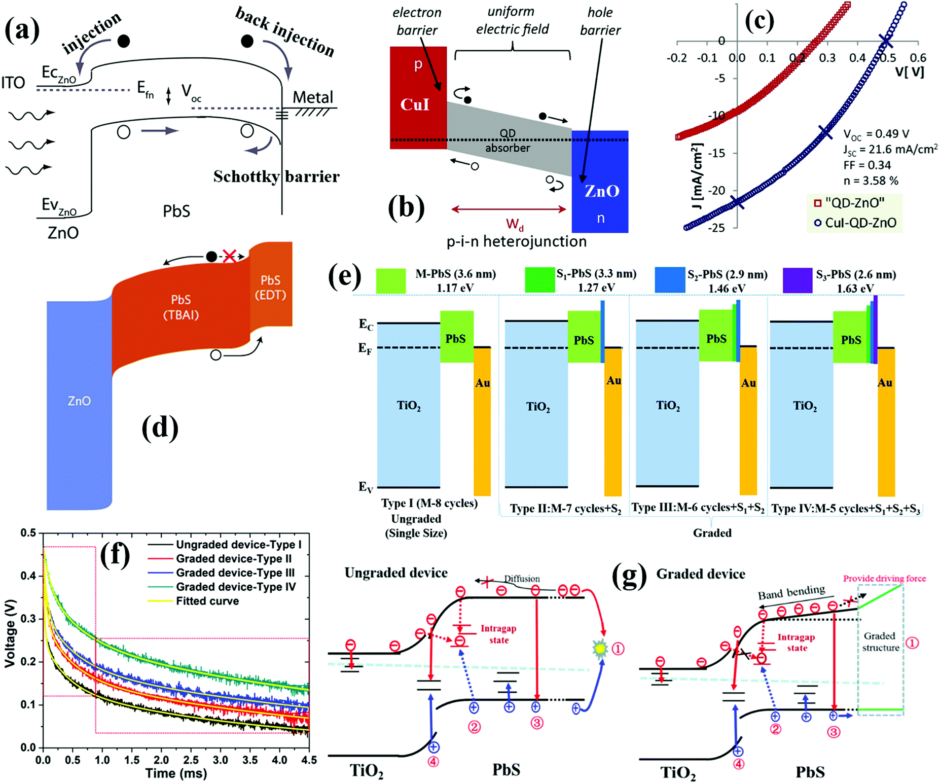 | ||
| Fig. 22 (a) Energy band diagram of an ITO/ZnO/PbS QDs/metal electrode structure QDSCs with Schottky barrier under illumination. (b) Schematic energy level diagram of p–i–n sandwiched structure PDHJ-QDSCs. The depletion width is denoted by wd and the black dotted line represents the equilibrium Fermi level. (c) J–V curves of QDSCs with and without CuI as HSL. (d) Schematic of ZnO/PbS-TBAI/PbS-EDT/Au architecture QDSCs. (e) Energy band diagrams of ungraded and graded QDSCs. The thickness of QDs active layer in those devices is the same. (f) The normalized TPV decay curves for ungraded and graded PbS QDSCs. (g) Possible carrier recombination paths in ungraded and graded QDSCs. Path (1) carrier recombination at PbS QDs/Au interface, (2) trap-state-assisted carrier recombination, (3) directly band-to-band carrier recombination, and (4) carrier recombination at ETL(TiO2)/PbS QDs. (a) Adapted with permission from ref. 298. Copyright (2011) American Chemical Society. (b and c) Reprinted with permission from ref. 301. Copyright (2014) Wiley. (d) Reprinted with permission from ref. 302. Copyright (2014) Springer Nature. (e–g) Reprinted with permission from ref. 307. Copyright (2018) American Chemical Society. | ||
With the purpose of increasing the hole extraction and reducing the electron back injection from the QD layer into the Au electrode, the insertion of a p-type thin hole selective interlayer (HSL) between the QD layer and the top metal contact to construct a graded structure has been proved efficiently to inhibit the Schottky contact (Fig. 1e). The insertion of a thin HSL at the QDs/Au interface in QDSCs was first carried out by Aydil and coworkers, in which they used a thin N,N′-bis(1-naphthalenyl)-N,N′-bis(phenylbenzidine) (α-NPD) layer (15–30 nm) to protect the back injection of photogenerated electrons from the PbSe QD to the Au electrode.198 After that, Brown et al. introduced a high work function inorganic semiconductor, MoO3, as the HSL into PbS QDSCs.199 The insertion of MoO3 pinned the Fermi level of the metal electrode enabling the formation of an Ohmic contact to PbS QDs and leads to an enhancement in the JSC, FF and VOC of the device. Bawendi and coworker reported a p–i–n graded structure planar depleted-heterojunction (PDHJ)-QDSCs by using ZnO as n-type ETL, 1,3-BDT treated PbS QDs as an intrinsic absorber layer, and p-type CuI with a small electron affinity (2.1 eV) and a high hole mobility (1.1 cm2 V−1 s−1) as HSL (Fig. 22b).301 This p–i–n heterojunction design demonstrates an enhancement in the depletion width and built-in potential, and inhibits the formation of Schottky contact at QDs/Au interface which leads to an improved carrier collection (larger JSC) and a higher VOC (Fig. 22c). The surface composition of the QD affects the doping types and densities of the QD solid film (Fig. 12b).19 By using a surface ligand doping strategy, Sargent and coworker designed n+–n–p+ and p+–p–n structures to broaden the width of the depletion region and reduce electron back injection at the QD/metal electrode interface.186,202 What needs to be highlighted is that Bawendi and coworker deposited a top EDT-capped p-type PbS QD film onto a TBAI treated PbS QD film to build up a classic p–i–n graded structure QDSC (Fig. 22d).302 The introduction of the thin EDT-treated QD layer causes additional band bending at the QDs/Au interface, which prevents the formation of a Schottky barrier and suppresses the back injection of electrons at the QDs/Au interface, thus leading to an enhancement of VOC, JSC and FF. Based on the quantum size effect of QD, graded architecture can be fabricated in QDSCs using different sizes of QDs through energy-level gradient engineering.303–306 The dynamic of carrier transfer and recombination in the graded structure QDSCs has been investigated in our recent work (Fig. 22e).307Fig. 22f shows the TPV decay curves for ungraded and graded PbS based planar-DHJ QDSCs. The curves of graded structure devices reduced slowly compared with the ungraded structure device, and the calculated free carrier average lifetimes which obtained by fitting these decay curves for graded devices are 4.6 ms (type II), 6.1 ms (type III), and 7.1 ms (type IV), respectively. In contrast, the free carrier average lifetime in an ungraded device is 3.4 ms. The long free carrier lifetime in the graded structure devices indicates the low carrier recombination in these devices. We consider that the graded structure helps to reduce the carrier recombination in QDSCs through the two following ways. Firstly, the thin small-size QDs layer in the graded structure acts as an electron blocking layer to suppress the carrier recombination at the PbS QDs/Au electrode interface. Secondly, the graded structure is beneficial for driving more carriers to the electron transport layer (ETL) and metal electrode, and the existing trap-states in the device can be then filled with the additional carriers, thus reducing the trap-states assisted carrier recombination in the QDSCs device (Fig. 22g).
Recently, several organic hole transport materials have been employed as a hole selective layer (HSL)/electron blocking layer into QDSCs. Zhang et al. reported an organic–inorganic hybrid p–i–n architecture QDSC by using poly(3-hexylthiophene-2,5-diyl) (P3HT) as HSL.300 The addition of P3HT layer can efficiently reduce the carrier recombination at the PbS QDs/Au interface, which results in larger free electron lifetime in the device (Fig. 23a) and larger VOC (Fig. 23b). Furthermore, the formation of p-i heterojunction at the QDs/P3HT interface leads to an increased depletion region promoting photoexcited carrier extraction. Besides, 2,2′,7,7′-tetrakis(N,N-di-p-methoxyphenylamine)-9,9′-spirobifluorene (spiro-OMeTAD) and poly[bis(4-phenyl)(2,4,6-trimethylphenyl)amine] (PTAA) were also tried to be inserted into the PbS QDs/Au interface. However, a hole injection barrier is formed at this interface due to the unmatched energy levels of the QD and organic materials. Our group and coworker developed a novel organic small molecule, named BTPA-4, as an HSL in bulk depleted-heterojunction (BDHJ)-QDSCs (Fig. 1c and 23c).33 The VOC and PCE of the QDSCs are significantly improved after introducing BTPA-4 as the HSL. The TPV decay result reveals the effect of BTPA-4 as the HSL on carrier recombination in QDSCs. After fitting and analyzing the TPV decay curves, we consider that the relatively slow VOC decay process (Fig. 23d) and larger effective free carrier lifetime (Fig. 23e) of the device with BTPA-4 is caused by the reduced carrier recombination at the QDs/Au interface. Impedance spectroscopy was also used to reveal the carrier recombination mechanism in the QDSCs with and without BTPA-4. After fitting the impedance spectra of these devices using an equivalent circuit (Fig. 23f), the carrier recombination resistance (Rrec) at the QDs/Au interface is obtained (Fig. 23g). Since the Rrec is inversely proportional to the carrier recombination rate,238,273 the larger Rrec in the QDSCs with BTPA-4 as the HSL confirms the slower carrier recombination rate in the devices. This is consistent with the result of TPV decay measurement (Fig. 23d). Subsequently, a p-doped small molecular N,N,N′,N′′-tetrakis(4-methoxyphenyl)-benzidine (MeOTPD) is employed as HSL to remove Schottky barrier at PbS QDs/Ag electrode interface and prevent water and oxygen to be permeated into the QD layer.308 The suitable energy level and hydro/oxo-phobic property of the p-MeOTPD layer efficiently improve the hole extraction and suppress electron back injection at the QDs/Ag interface which leads to a high PCE of 11.7%, while excellent storage stability performance is also achieved. Currently, a high hole mobility polymer (8.5 × 10⁻⁴ cm2 V−1 s−1), polythieno[3,4-b]-thiophene-co-benzodithiophene (PTB7), is also used as an HSL in QDSCs.309 Due to the more favorable energy levels, higher hole mobility, and photogenerated dipole effect of PTB7, the QDSCs using PTB7 exhibits superior photovoltaic performance (with a PCE of 9.6%) than those using P3HT. Notably, the intensity modulated photovoltage spectroscopy (IMVS, Fig. 23h) and the intensity modulated photocurrent spectroscopy (IMPS, Fig. 23i) are used to investigate the dynamic of photoexcited carrier recombination and hole extraction at QDs/HSL/Ag interface, respectively. The obtained free carrier lifetime of the QDSCs with PTB7 from IMVS is longer (1.58 μs) than that of the QDSCs with P3HT (1.30 μs), indicating the suppressed carrier recombination at QDs/HSL/Ag junctions. While the calculated carrier transport time from IMPS for the QDSCs with PTB7 is shorter (0.30 μs) than that of the QDSCs with P3HT (0.35 μs), revealing the faster hole extraction in PTB7-based device. Although the free carrier lifetimes are in the microsecond region obtained from IMVS or IMPS different from the previous TPV decay results, it is sure enough that introducing a hole selective layer between the QDs and metal electrode can effectively reduce the interfacial recombination. Finally, a relatively higher carrier collection efficiency of 0.81 is achieved in PTB7-based QDSCs due to the improved carrier transport and reduced carrier recombination at the QDs/Ag electrode interface.
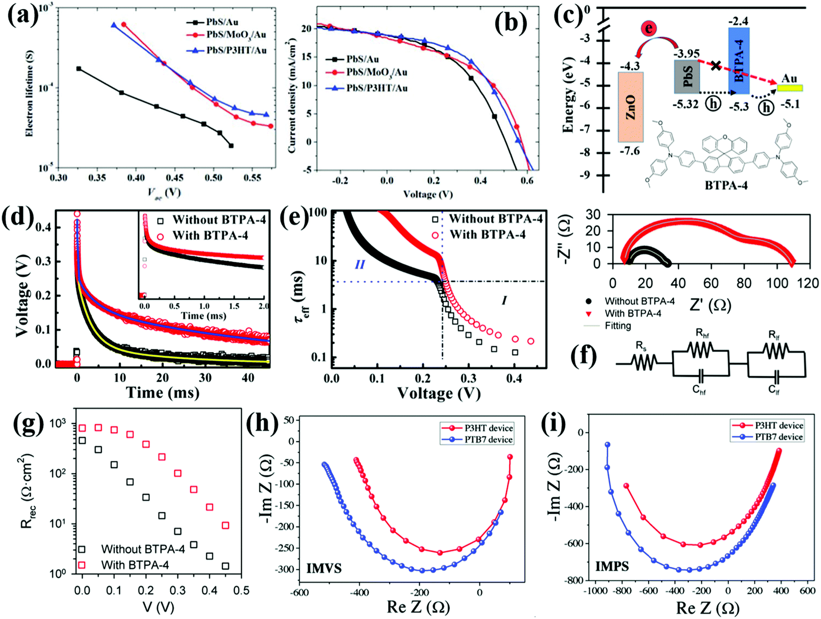 | ||
| Fig. 23 (a) Free electron lifetime as a function of VOC for the QDSCs without any HSL and with MoO3 or P3HT as HSL. (b) J–V curves of the QDSCs without any HSL and with MoO3 or P3HT as HSL. (c) Molecular structure of BTPA-4 (bottom), and schematic energy level diagram of the ZnO, PbS QDs, BTPA-4 and Au (top). (d) TPV decay curves of the QDSCs without and with BTPA-4. (e) Effective carrier lifetime (τeff) of PbS QDSCs without and with BTPA-4 that are calculated from the TPV decay curves shown in panel (d). (f) Nyquist plots of PbS QDSCs with and without BTPA-4 in dark with 0.3 V applied bias (top) and the equivalent circuit of the device (bottom). (g) Recombination resistance (Rrec) of QDSCs with and without BTPA-4 obtained by impedance spectroscopy under different applied bias. (h) The intensity modulated photovoltage spectroscopy (IMVS) of QDSCs with P3HT and PTB7 as HSL. (i) The intensity-modulated photocurrent spectroscopy (IMPS) of QDSCs with P3HT and PTB7 as HSL. (a and b) Reprinted with permission from ref. 300. Copyright (2015) Royal Society of Chemistry. (c–g) Reprinted with permission from ref. 33. Copyright (2017) American Chemical Society. (h and i) Reprinted with permission from ref. 309. Copyright (2018) Wiley. | ||
Nowadays, the electron transfer and carrier recombination dynamics at the electron transport layer (ETL)/QDs interface have been well investigated. Based on Marcus theory, the electron transfer dynamics from QD to ETL can be affected by the Gibbs free energy change (ΔG) between the QD and ETL, ETL–QD distance, and electron affinity of the ETL materials etc. Although the insertion of a buffer layer can suppress the interfacial carrier recombination at both the ETL/QDs and QDs/metal electrode interfaces, photoexcited carrier transfer or extraction at those interfaces are also adversely affected. Thus, it is necessary to balance the competitive effect between reduced interfacial recombination and enhanced carrier transfer or extraction in the QDSC device. In addition, the hole transfer dynamics in QDSCs have not been studied in depth, especially in typical depleted-heterojunction QDSCs. More attention should be paid to the study of hole transfer dynamics in the future.
6. Conclusions and perspectives
Rapid progress has been made in the field of QDSCs over the past decade, and the certified power conversion efficiency (PCE) of QDSCs has considerably improved from below 4% to recent 16.6%. This impressive improvement has been achieved mainly via QD surface engineering, interface passivation and new designing of device architectures. The study of photoexcited carrier dynamics in QDSCs can help to recognize and understand the essential mechanisms of the present and potential problems that affect the generation, extraction and recombination processes of carriers, and provide guidance for improving the photovoltaic performance of QDSCs. Recent related research about photoexcited carrier dynamics in the QDSCs starting from individual QDs via QD solid film to the interface of the device as well as the characterization methods used for analyzing the photoexcited carrier dynamics have been summarized and discussed in this review. The factors affecting carrier generation, extraction, and recombination have been summarized according to the reported experimental results and basic physics models.The optimal PCEs of sensitized QDSCs, Pb chalcogenide-based QDSCs, and perovskite-based QDSCs have been achieved to 13.5%,23 12.48%,218 and 16.6%,18 respectively, while these values are still lower than that of silicon solar cells and bulk perovskite solar cells, not to mention the theoretical efficiency of QDSCs. The high-density surface trap-states in QD, multiple sub-bandgap states and energy disorder in QDs solid film, and serious carrier recombination at interfaces induce significantly poor carrier extraction or collection and large VOC deficit, which seriously limit the photovoltaic performance of QDSCs. It is imperative to develop novel passivation strategies and efficient structural design to improve the photovoltaic performance of QDSCs. Therefore, we believe that the following aspects are key issues for the future development of QDSCs through enhancing charge generation, separation and collection efficiency, and minimizing the recombination.
(1) Synthesis of high-quality QDs with ideal properties
It would be beneficial to prepare QDs with good monodispersity in order to suppress the undesired energy transfer between adjacent QDs and reduce the extent of energy level pinning in QD solid films. Thus, studies of the nucleation and growth process of QDs by changing the reaction material and their ratio, reaction temperature and time should be well investigated in the future. Although the quality of QDs has been significantly improved by various surface passivation technologies, the photoluminescence quantum yield (PLQY) values of most QDs are still below 100%, which indicates that serious trap-states still exist in those QDs. Exploring novel surface passivation strategies for QDs, such as iodine-based hybrid ligand systems, thin shell passivation, and self-repair technologies, will probably reduce the surface trap-state density, enhance the PLQY as high as 100%, and elongate the lifetime of photogenerated excitons, especially the lifetime of hot excitons.(2) Extraction of multiple excitons and hot excitons
As one of the most attractive physical properties of QDs, the multiple exciton generation (MEG) phenomenon has been observed in many QDs. Unfortunately, only a few reported devices achieved over 100% monochromatic incident photon-to-electron conversion efficiency (IPCE) but only in the UV region. Due to the fast cooling rate, hot electrons and holes are difficult to be extracted before cooling or trapping. Thus, the research of hot exciton based QDSCs still stays in the theoretical stage. Exploring novel narrow bandgap QD semiconductors with visible light MEG response and new materials with much smaller effective electron mass compared to the effective hole mass, will benefit to generate more excitons in a wide incident light spectrum. Studies of novel electron transport layer (ETL) [or hole selective layer (HSL)] with high electron (or hole) affinity will be in favor of extracting multiple excitons and hot electrons (holes) from QDs before their recombination. Similar sensitization architecture of QDSCs has great potential to realize the effective extraction of multiple excitons and hot excitons due to the direct contact between the ETL and QDs with the shortest carrier transport length.(3) Novel ligand exchange and QD active layer deposition strategies
As the most important part of QDSCs, the electrical properties and stability of the QD active layer play a decisive role in the performance of the devices. During the ligand exchange process, the surface trap and the sub-bandgap states of QDs can be inevitably introduced. Thus, it is urgent to minimize the introduction of trap-states in the QD active layers, enhance the QD coupling, increase the photoexcited electron–hole separation and transfer efficiency, and improve the lifetime and diffusion length of free carriers by exploring novel ligand exchange strategies, such as hybrid ligand passivation systems, the less use of protic solvent, and new solution-state ligand exchange systems. Simple, efficient and economical QD active layer deposition methods such as one-step spin-coating, scraping or screen-printing method need to be further optimized and explored.(4) Bulk depleted-heterojunction architecture
The thickness of the QD active layer is usually limited to about 500 nm due to the short free carrier diffusion length in the QD solid film which reduces the absorption efficiency of incident light. Designing new bulk heterojunction structure QDSCs or introducing a one-dimensional (1D) or 2D carrier transport material into the QD active layer is conducive to carrier transport and reducing carrier recombination with a much thicker QD active layer, which can directly improve the JSC and reduce the VOC deficit of the device.(5) Optimization of electron transport layer and hole selective layer
As the carrier collection and recombination centers, the quality and electrical performance of both the ETL and HSL greatly affect the photovoltaic performance of QDSCs. New ETL and HSL design should be developed to improve the charge-carrier collection efficiency at the ETL/QDs and QDs/HSL/metal electrode interface but with diminished recombination occurring at these interfaces. It needs to be emphasized that there is still little research in the field of the dynamics of hole transfer or extraction in QDSCs nowadays, and more attention needs to be paid to this field in the future for QDSCs.Conflicts of interest
There are no conflicts to declare.Acknowledgements
This work was supported by the MEXT KAKENHI grant (Grands 26286013, 17H02736), JSPS International Research Fellow (Faculty of Informatics and Engineering, UEC). G.W. acknowledges the Natural Science Foundation of Shaanxi Province (2019JQ-423), the Fundamental Research Funds for the Central Universities (GK201903053), and the Key Lab of photovoltaic and Energy Conservation Materials, Chinese Academy of Sciences (No. PECL2019KF019) for financial support.References
- J. Shi, Y. Li, Y. Li, D. Li, Y. Luo, H. Wu and Q. Meng, Joule, 2018, 2, 879–901 CrossRef CAS.
- S. N. Yun, Y. Qin, A. R. Uhl, N. Vlachopoulos, M. Yin, D. D. Li, X. G. Han and A. Hagfeldt, Energy Environ. Sci., 2018, 11, 476–526 RSC.
- C. B. Murray, D. J. Norris and M. G. Bawendi, J. Am. Chem. Soc., 1993, 115, 8706–8715 CrossRef CAS.
- A. P. Alivisatos, Science, 1996, 271, 933–937 CrossRef CAS.
- I. Moreels, K. Lambert, D. Smeets, D. De Muynck, T. Nollet, J. C. Martins, F. Vanhaecke, A. Vantomme, C. Delerue, G. Allan and Z. Hens, ACS Nano, 2009, 3, 3023–3030 CrossRef CAS PubMed.
- Q. Dai, Y. Wang, X. Li, Y. Zhang, D. J. Pellegrino, M. Zhao, B. Zou, J. Seo, Y. Wang and W. W. Yu, ACS Nano, 2009, 3, 1518–1524 CrossRef CAS PubMed.
- S. A. McDonald, G. Konstantatos, S. Zhang, P. W. Cyr, E. J. D. Klem, L. Levina and E. H. Sargent, Nat. Mater., 2005, 4, 138–142 CrossRef CAS PubMed.
- A. J. Nozik, Phys. E, 2002, 14, 115–120 CrossRef CAS.
- R. J. Ellingson, M. C. Beard, J. C. Johnson, P. Yu, O. I. Micic, A. J. Nozik, A. Shabaev and A. L. Efros, Nano Lett., 2005, 5, 865–871 CrossRef CAS PubMed.
- M. R. Kim and D. Ma, J. Phys. Chem. Lett., 2015, 6, 85–99 CrossRef CAS PubMed.
- W. Shockley and H. J. Queisser, J. Appl. Phys., 1961, 32, 510–519 CrossRef CAS.
- J. Jean, J. Xiao, R. Nick, N. Moody, M. Nasilowski, M. Bawendi and V. Bulovic, Energy Environ. Sci., 2018, 11, 2295–2305 RSC.
- C. S. Ponseca, P. Chábera, J. Uhlig, P. Persson and V. Sundström, Chem. Rev., 2017, 117, 10940–11024 CrossRef CAS PubMed.
- Y. Kuang, K. Sun, S. Sukrittanon, K. Takabayashi, I. Kamiya, N. S. Lewis and C. W. Tu, Nano Energy, 2015, 15, 782–788 CrossRef CAS.
- R. Wang, X. Wu, K. Xu, W. Zhou, Y. Shang, H. Tang, H. Chen and Z. Ning, Adv. Mater., 2018, 30, 1704882 CrossRef PubMed.
- J. Albero, J. N. Clifford and E. Palomares, Coord. Chem. Rev., 2014, 263–264, 53–64 CrossRef CAS.
- A. Zaban, O. I. Mićić, B. A. Gregg and A. J. Nozik, Langmuir, 1998, 14, 3153–3156 CrossRef CAS.
- NREL, Research Cell Record Efficiency Chart, National Renewable Energy Laboratory, https://www.nrel.gov/pv/cell-efficiency.html, accessed Augest 2019.
- R. Wang, Y. Shang, P. Kanjanaboos, W. Zhou, Z. Ning and E. H. Sargent, Energy Environ. Sci., 2016, 9, 1130–1143 RSC.
- X. L. Zhang, C. Hagglund and E. M. J. Johansson, Energy Environ. Sci., 2017, 10, 216–224 RSC.
- H. Aqoma and S.-Y. Jang, Energy Environ. Sci., 2018, 11, 1603–1609 RSC.
- S. Paulo, E. Palomares and E. Martinez-Ferrero, Nanomaterials, 2016, 6, 157 CrossRef PubMed.
- W. Wang, L. Zhao, Y. Wang, W. Xue, F. He, Y. Xie and Y. Li, J. Am. Chem. Soc., 2019, 141, 4300–4307 CrossRef CAS PubMed.
- G. Shi, A. Kaewprajak, X. Ling, A. Hayakawa, S. Zhou, B. Song, Y. Kang, T. Hayashi, M. E. Altun, M. Nakaya, Z. Liu, H. Wang, T. Sagawa and W. Ma, ACS Energy Lett., 2019, 4, 960–967 CrossRef CAS.
- G. H. Carey, A. L. Abdelhady, Z. Ning, S. M. Thon, O. M. Bakr and E. H. Sargent, Chem. Rev., 2015, 115, 12732–12763 CrossRef CAS PubMed.
- Z. Liu, J. Yuan, S. A. Hawks, G. Shi, S.-T. Lee and W. Ma, Sol. RRL, 2017, 1, 1600021 CrossRef.
- H. Zhao and F. Rosei, Chem, 2017, 3, 229–258 CAS.
- K. Das and B. Sunandan, Curr. Sci., 2018, 115, 659–668 CrossRef CAS.
- M. C. Hanna and A. J. Nozik, J. Appl. Phys., 2006, 100, 074510 CrossRef.
- M. C. Beard, A. G. Midgett, M. C. Hanna, J. M. Luther, B. K. Hughes and A. J. Nozik, Nano Lett., 2010, 10, 3019–3027 CrossRef CAS PubMed.
- A. J. Nozik, Nano Lett., 2010, 10, 2735–2741 CrossRef CAS PubMed.
- P. V. Kamat, Acc. Chem. Res., 2012, 45, 1906–1915 CrossRef CAS PubMed.
- Y. Zhang, G. Wu, I. Mora-Seró, C. Ding, F. Liu, Q. Huang, Y. Ogomi, S. Hayase, T. Toyoda, R. Wang, J. Otsuki and Q. Shen, J. Phys. Chem. Lett., 2017, 8, 2163–2169 CrossRef CAS PubMed.
- J. Y. Xu, X. Tong, P. Yu, G. E. Wenya, T. McGrath, M. J. Fong, J. Wu and Z. M. Wang, Adv. Sci., 2018, 5, 1800221 CrossRef PubMed.
- W. A. Tisdale, PhD thesis, University of Minnesota, 2010.
- J. Shah, Ultrafast Spectroscopy of Semiconductors and Semiconductor Nanostructures, Springer, New York, 1996 Search PubMed.
- M. C. Beard and R. J. Ellingson, Laser Photonics Rev., 2008, 2, 377–399 CrossRef CAS.
- A. Mysyrowicz, D. Hulin, A. Antonetti, A. Migus, W. T. Masselink and H. Morkoç, Phys. Rev. Lett., 1986, 56, 2748–2751 CrossRef CAS PubMed.
- A. Von Lehmen, D. S. Chemla, J. E. Zucker and J. P. Heritage, Opt. Lett., 1986, 11, 609–611 CrossRef CAS PubMed.
- Y. Yang, D. P. Ostrowski, R. M. France, K. Zhu, J. van de Lagemaat, J. M. Luther and M. C. Beard, Nat. Photonics, 2015, 10, 53 CrossRef.
- J. Chen, M. E. Messing, K. Zheng and T. Pullerits, J. Am. Chem. Soc., 2019, 141, 3532–3540 CrossRef CAS PubMed.
- K. Katayama, M. Yamaguchi and T. Sawada, Appl. Phys. Lett., 2003, 82, 2775–2777 CrossRef CAS.
- N. Maeda, H. Hata, N. Osada, Q. Shen, T. Toyoda, S. Kuwahara and K. Katayama, Phys. Chem. Chem. Phys., 2013, 15, 11006–11013 RSC.
- N. Osada, T. Oshima, S. Kuwahara, T. Toyoda, Q. Shen and K. Katayama, Phys. Chem. Chem. Phys., 2014, 16, 5774–5778 RSC.
- M. Ebihara, W. Y. Sohn and K. Katayama, Rev. Sci. Instrum., 2019, 90, 073905 CrossRef PubMed.
- J. A. Rogers and K. A. Nelson, J. Appl. Phys., 1994, 75, 1534–1556 CrossRef CAS.
- L. Dhar, J. A. Rogers and K. A. Nelson, Chem. Rev., 1994, 94, 157–193 CrossRef CAS.
- K. Katayama, Y. Inagaki and T. Sawada, J. Appl. Phys., 2002, 92, 5233–5237 CrossRef CAS.
- Q. Shen, K. Katayama and T. Toyoda, J. Energy Chem., 2015, 24, 712–716 CrossRef.
- K. Zhao, Z. Pan, I. Mora-Sero, E. Canovas, H. Wang, Y. Song, X. Gong, J. Wang, M. Bonn, J. Bisquert and X. Zhong, J. Am. Chem. Soc., 2015, 137, 5602–5609 CrossRef CAS PubMed.
- M. R. Bergren, P. K. B. Palomaki, N. R. Neale, T. E. Furtak and M. C. Beard, ACS Nano, 2016, 10, 2316–2323 CrossRef CAS PubMed.
- G. Nair, S. M. Geyer, L. Chang and M. G. Bawendi, Phys. Rev. B: Condens. Matter Mater. Phys., 2008, 78, 125325 CrossRef.
- A. J. Nozik, Annu. Rev. Phys. Chem., 2001, 52, 193–231 CrossRef CAS PubMed.
- A. J. Nozik and O. I. Mićić, Quantum Dots and Quantum Dot Arrays: Synthesis, Optical Properties, Photogenerated CarrierDynamics, Multiple Exciton Generation, and Applications to Solar Photon Conversion, CRC Press, Boca Raton, 2nd edn, 2017 Search PubMed.
- A. Nevin, A. Cesaratto, S. Bellei, C. D’Andrea, L. Toniolo, G. Valentini and D. Comelli, Sensors, 2014, 14, 6338–6355 CrossRef CAS PubMed.
- B. C. O'Regan and J. R. Durrant, J. Phys. Chem. B, 2006, 110, 8544–8547 CrossRef PubMed.
- O. J. Sandberg, K. Tvingstedt, P. Meredith and A. Armin, J. Phys. Chem. C, 2019, 123, 14261–14271 CrossRef CAS.
- A. Zaban, M. Greenshtein and J. Bisquert, ChemPhysChem, 2003, 4, 859–864 CrossRef CAS PubMed.
- A. J. Nozik, Chem. Phys. Lett., 2008, 457, 3–11 CrossRef CAS.
- O. E. Semonin, J. M. Luther, S. Choi, H.-Y. Chen, J. Gao, A. J. Nozik and M. C. Beard, Science, 2011, 334, 1530–1533 CrossRef CAS PubMed.
- M. L. Böhm, T. C. Jellicoe, M. Tabachnyk, N. J. L. K. Davis, F. Wisnivesky-Rocca-Rivarola, C. Ducati, B. Ehrler, A. A. Bakulin and N. C. Greenham, Nano Lett., 2015, 15, 7987–7993 CrossRef PubMed.
- Y. Yan, R. W. Crisp, J. Gu, B. D. Chernomordik, G. F. Pach, Ashley R. Marshall, J. A. Turner and M. C. Beard, Nat. Energy, 2017, 2, 17052 CrossRef CAS.
- J. H. Werner, S. Kolodinski and H. J. Queisser, Phys. Rev. Lett., 1994, 72, 3851–3854 CrossRef CAS PubMed.
- A. Kryjevski, D. Mihaylov and D. Kilin, J. Phys. Chem. Lett., 2018, 9, 5759–5764 CrossRef CAS PubMed.
- A. G. Midgett, PhD thesis, University of Colorado, Boulder, 2011.
- A. J. Neukirch, K. Hyeon-Deuk and O. V. Prezhdo, Coord. Chem. Rev., 2014, 263–264, 161–181 CrossRef CAS.
- T. T. Ngo and I. Mora-Seró, J. Phys. Chem. Lett., 2019, 10, 1099–1108 CrossRef CAS PubMed.
- M. C. Beard, J. Phys. Chem. Lett., 2011, 2, 1282–1288 CrossRef CAS PubMed.
- C. Smith and D. Binks, Nanomaterials, 2014, 4, 19–45 CrossRef PubMed.
- M. Li, R. Begum, J. Fu, Q. Xu, T. M. Koh, S. A. Veldhuis, M. Grätzel, N. Mathews, S. Mhaisalkar and T. C. Sum, Nat. Commun., 2018, 9, 4197 CrossRef PubMed.
- R. D. Schaller and V. I. Klimov, Phys. Rev. Lett., 2004, 92, 186601 CrossRef CAS PubMed.
- M. T. Trinh, A. J. Houtepen, J. M. Schins, T. Hanrath, J. Piris, W. Knulst, A. P. L. M. Goossens and L. D. A. Siebbeles, Nano Lett., 2008, 8, 1713–1718 CrossRef PubMed.
- Y. Yang, W. Rodríguez-Córdoba and T. Lian, Nano Lett., 2012, 12, 4235–4241 CrossRef CAS PubMed.
- R. D. Schaller, M. Sykora, J. M. Pietryga and V. I. Klimov, Nano Lett., 2006, 6, 424–429 CrossRef CAS PubMed.
- M. Ono, T. Nishihara, T. Ihara, M. Kikuchi, A. Tanaka, M. Suzuki and Y. Kanemitsu, Chem. Sci., 2014, 5, 2696–2701 RSC.
- M. Kumar, S. Vezzoli, Z. Wang, V. Chaudhary, R. V. Ramanujan, G. G. Gurzadyan, A. Bruno and C. Soci, Phys. Chem. Chem. Phys., 2016, 18, 31107–31114 RSC.
- F. C. M. Spoor, G. Grimaldi, C. Delerue, W. H. Evers, R. W. Crisp, P. Geiregat, Z. Hens, A. J. Houtepen and L. D. A. Siebbeles, ACS Nano, 2018, 12, 4796–4802 CrossRef CAS PubMed.
- G. Nair and M. G. Bawendi, Phys. Rev. B: Condens. Matter Mater. Phys., 2007, 76, 081304 CrossRef.
- T. Ichibayashi and K. Tanimura, Phys. Rev. Lett., 2009, 102, 087403 CrossRef CAS.
- Q. Shen, K. Katayama, T. Sawada, S. Hachiya and T. Toyoda, Chem. Phys. Lett., 2012, 542, 89–93 CrossRef CAS.
- T. Sjodin, H. Petek and H.-L. Dai, Phys. Rev. Lett., 1998, 81, 5664–5667 CrossRef CAS.
- P. Kužel, F. Kadlec and H. Němec, J. Chem. Phys., 2007, 127, 024506 CrossRef PubMed.
- S. V. Kershaw and A. L. Rogach, Materials, 2017, 10, 1095 CrossRef PubMed.
- J. E. Murphy, M. C. Beard, A. G. Norman, S. P. Ahrenkiel, J. C. Johnson, P. Yu, O. I. Mićić, R. J. Ellingson and A. J. Nozik, J. Am. Chem. Soc., 2006, 128, 3241–3247 CrossRef CAS PubMed.
- R. D. Schaller, M. A. Petruska and V. I. Klimov, Appl. Phys. Lett., 2005, 87, 253102 CrossRef.
- A. Franceschetti and Y. Zhang, Phys. Rev. Lett., 2008, 100, 136805 CrossRef PubMed.
- Z. Lin, A. Franceschetti and M. T. Lusk, ACS Nano, 2011, 5, 2503–2511 CrossRef CAS PubMed.
- R. D. Schaller, J. M. Pietryga and V. I. Klimov, Nano Lett., 2007, 7, 3469–3476 CrossRef CAS PubMed.
- S. K. Stubbs, S. J. O. Hardman, D. M. Graham, B. F. Spencer, W. R. Flavell, P. Glarvey, O. Masala, N. L. Pickett and D. J. Binks, Phys. Rev. B: Condens. Matter Mater. Phys., 2010, 81, 081303 CrossRef.
- C. M. Cirloganu, L. A. Padilha, Q. Lin, N. S. Makarov, K. A. Velizhanin, H. Luo, I. Robel, J. M. Pietryga and V. I. Klimov, Nat. Commun., 2014, 5, 4148 CrossRef CAS PubMed.
- D. M. Kroupa, G. F. Pach, M. Vörös, F. Giberti, B. D. Chernomordik, R. W. Crisp, A. J. Nozik, J. C. Johnson, R. Singh, V. I. Klimov, G. Galli and M. C. Beard, ACS Nano, 2018, 12, 10084–10094 CrossRef CAS PubMed.
- D. J. Vogel, A. Kryjevski, T. Inerbaev and D. S. Kilin, J. Phys. Chem. Lett., 2017, 8, 3032–3039 CrossRef CAS.
- C. de Weerd, L. Gomez, A. Capretti, D. M. Lebrun, E. Matsubara, J. Lin, M. Ashida, F. C. M. Spoor, L. D. A. Siebbeles, A. J. Houtepen, K. Suenaga, Y. Fujiwara and T. Gregorkiewicz, Nat. Commun., 2018, 9, 4199 CrossRef PubMed.
- M. Gordi, H. Ramezani and M. K. Moravvej-Farshi, J. Phys. Chem. C, 2017, 121, 6374–6379 CrossRef CAS.
- S. Saeed, C. de Weerd, P. Stallinga, F. C. M. Spoor, A. J. Houtepen, L. Da Siebbeles and T. Gregorkiewicz, Light: Sci. Appl., 2015, 4, e251 CrossRef CAS.
- M. T. Trinh, R. Limpens, W. D. A. M. de Boer, J. M. Schins, L. D. A. Siebbeles and T. Gregorkiewicz, Nat. Photonics, 2012, 6, 316–321 CrossRef CAS.
- M. C. Beard, K. P. Knutsen, P. Yu, J. M. Luther, Q. Song, W. K. Metzger, R. J. Ellingson and A. J. Nozik, Nano Lett., 2007, 7, 2506–2512 CrossRef CAS PubMed.
- L. A. Padilha, J. T. Stewart, R. L. Sandberg, W. K. Bae, W.-K. Koh, J. M. Pietryga and V. I. Klimov, Acc. Chem. Res., 2013, 46, 1261–1269 CrossRef CAS PubMed.
- P. Tyagi and P. Kambhampati, J. Chem. Phys., 2011, 134, 094706 CrossRef PubMed.
- J. A. McGuire, J. Joo, J. M. Pietryga, R. D. Schaller and V. I. Klimov, Acc. Chem. Res., 2008, 41, 1810–1819 CrossRef CAS PubMed.
- M. C. Beard, A. G. Midgett, M. Law, O. E. Semonin, R. J. Ellingson and A. J. Nozik, Nano Lett., 2009, 9, 836–845 CrossRef CAS PubMed.
- F. W. Wise, Acc. Chem. Res., 2000, 33, 773–780 CrossRef CAS PubMed.
- J. W. Haus, H. S. Zhou, I. Honma and H. Komiyama, Phys. Rev. B: Condens. Matter Mater. Phys., 1993, 47, 1359–1365 CrossRef CAS PubMed.
- A. G. Midgett, J. M. Luther, J. T. Stewart, D. K. Smith, L. A. Padilha, V. I. Klimov, A. J. Nozik and M. C. Beard, Nano Lett., 2013, 13, 3078–3085 CrossRef CAS PubMed.
- H. Kamisaka, S. V. Kilina, K. Yamashita and O. V. Prezhdo, J. Phys. Chem. C, 2008, 112, 7800–7808 CrossRef CAS.
- T. Schwarzl, E. Kaufmann, G. Springholz, K. Koike, T. Hotei, M. Yano and W. Heiss, Phys. Rev. B: Condens. Matter Mater. Phys., 2008, 78, 165320 CrossRef.
- R. G. Wheeler and J. O. Dimmock, Phys. Rev., 1962, 125, 1805–1815 CrossRef CAS.
- S. Tamang, C. Lincheneau, Y. Hermans, S. Jeong and P. Reiss, Chem. Mater., 2016, 28, 2491–2506 CrossRef CAS.
- M. S. Gudiksen, J. Wang and C. M. Lieber, J. Phys. Chem. B, 2002, 106, 4036–4039 CrossRef CAS.
- L. Protesescu, S. Yakunin, M. I. Bodnarchuk, F. Krieg, R. Caputo, C. H. Hendon, R. X. Yang, A. Walsh and M. V. Kovalenko, Nano Lett., 2015, 15, 3692–3696 CrossRef CAS PubMed.
- U.-G. Jong, C.-J. Yu, Y.-S. Kim, Y.-H. Kye and C.-H. Kim, Phys. Rev. B, 2018, 98, 125116 CrossRef CAS.
- H. D. Barber, Solid-State Electron., 1967, 10, 1039–1051 CrossRef CAS.
- Y. Maeda, N. Tsukamoto, Y. Yazawa, Y. Kanemitsu and Y. Masumoto, Appl. Phys. Lett., 1991, 59, 3168–3170 CrossRef CAS.
- X. Peng, F. Tang and P. Logan, Handbook of Nanomaterials Properties: Electronic Properties of Si and Ge Pure and Core-Shell Nanowires from First Principle Study, Springer, Berlin Heidelberg, 2014 Search PubMed.
- M. C. Beard, J. M. Luther, O. E. Semonin and A. J. Nozik, Acc. Chem. Res., 2013, 46, 1252–1260 CrossRef CAS PubMed.
- R. T. Ross and A. J. Nozik, J. Appl. Phys., 1982, 53, 3813–3818 CrossRef CAS.
- R. López-Arteaga and J. Peon, J. Phys. Chem. C, 2018, 122, 26698–26706 CrossRef.
- P. Singhal and H. N. Ghosh, Chem. – Eur. J., 2015, 21, 4405–4412 CrossRef CAS PubMed.
- F. C. M. Spoor, L. T. Kunneman, W. H. Evers, N. Renaud, F. C. Grozema, A. J. Houtepen and L. D. A. Siebbeles, ACS Nano, 2016, 10, 695–703 CrossRef CAS PubMed.
- W. A. Tisdale, K. J. Williams, B. A. Timp, D. J. Norris, E. S. Aydil and X.-Y. Zhu, Science, 2010, 328, 1543–1547 CrossRef CAS PubMed.
- W. A. Tisdale and X.-Y. Zhu, Proc. Natl. Acad. Sci. U. S. A., 2011, 108, 965–970 CrossRef CAS PubMed.
- H. I. Wang, I. Infante, S. t. Brinck, E. Cánovas and M. Bonn, Nano Lett., 2018, 18, 5111–5115 CrossRef CAS PubMed.
- E. Cánovas, H. Wang, M. Karakus and M. Bonn, Chem. Phys., 2016, 471, 54–58 CrossRef.
- A. Boulesbaa, Z. Huang, D. Wu and T. Lian, J. Phys. Chem. C, 2010, 114, 962–969 CrossRef CAS.
- J. Huang, Z. Huang, Y. Yang, H. Zhu and T. Lian, J. Am. Chem. Soc., 2010, 132, 4858–4864 CrossRef CAS PubMed.
- N. Song, H. Zhu, S. Jin, W. Zhan and T. Lian, ACS Nano, 2011, 5, 613–621 CrossRef CAS PubMed.
- S. Jin and T. Lian, Sci. China: Chem., 2011, 54, 1898–1902 CrossRef CAS.
- H. Zhu, N. Song and T. Lian, J. Am. Chem. Soc., 2013, 135, 11461–11464 CrossRef CAS PubMed.
- H. Zhu, Y. Yang, K. Wu and T. Lian, Annu. Rev. Phys. Chem., 2016, 67, 259–281 CrossRef CAS PubMed.
- K. Wu, G. Liang, Q. Shang, Y. Ren, D. Kong and T. Lian, J. Am. Chem. Soc., 2015, 137, 12792–12795 CrossRef CAS PubMed.
- S. Sarkar, V. K. Ravi, S. Banerjee, G. R. Yettapu, G. B. Markad, A. Nag and P. Mandal, Nano Lett., 2017, 17, 5402–5407 CrossRef CAS PubMed.
- M. Li, S. Bhaumik, T. W. Goh, M. S. Kumar, N. Yantara, M. Grätzel, S. Mhaisalkar, N. Mathews and T. C. Sum, Nat. Commun., 2017, 8, 14350 CrossRef CAS PubMed.
- A. Pandey and P. Guyot-Sionnest, J. Phys. Chem. Lett., 2010, 1, 45–47 CrossRef CAS.
- H. Zhu, N. Song and T. Lian, J. Am. Chem. Soc., 2010, 132, 15038–15045 CrossRef CAS PubMed.
- G. Grimaldi, R. W. Crisp, S. ten Brinck, F. Zapata, M. van Ouwendorp, N. Renaud, N. Kirkwood, W. H. Evers, S. Kinge, I. Infante, L. D. A. Siebbeles and A. J. Houtepen, Nat. Commun., 2018, 9, 2310 CrossRef PubMed.
- T. X. Ding, J. H. Olshansky, S. R. Leone and A. P. Alivisatos, J. Am. Chem. Soc., 2015, 137, 2021–2029 CrossRef CAS PubMed.
- P. Kambhampati, J. Phys. Chem. C, 2011, 115, 22089–22109 CrossRef CAS.
- P. Kambhampati, Acc. Chem. Res., 2011, 44, 1–13 CrossRef CAS PubMed.
- A. Pandey and P. Guyot-Sionnest, Science, 2008, 322, 929–932 CrossRef CAS PubMed.
- P. Singhal and H. N. Ghosh, J. Phys. Chem. C, 2018, 122, 17586–17600 CrossRef CAS.
- F. C. M. Spoor, S. Tomić, A. J. Houtepen and L. D. A. Siebbeles, ACS Nano, 2017, 11, 6286–6294 CrossRef CAS PubMed.
- V. I. Klimov, D. W. McBranch, C. A. Leatherdale and M. G. Bawendi, Phys. Rev. B: Condens. Matter Mater. Phys., 1999, 60, 13740–13749 CrossRef CAS.
- D. A. Hines and P. V. Kamat, ACS Appl. Mater. Interfaces, 2014, 6, 3041–3057 CrossRef CAS PubMed.
- S. C. Boehme, J. M. Azpiroz, Y. V. Aulin, F. C. Grozema, D. Vanmaekelbergh, L. D. A. Siebbeles, I. Infante and A. J. Houtepen, Nano Lett., 2015, 15, 3056–3066 CrossRef CAS PubMed.
- B. Li, H. Huang, G. Zhang, C. Yang, W. Guo, R. Chen, C. Qin, Y. Gao, V. P. Biju, A. L. Rogach, L. Xiao and S. Jia, J. Phys. Chem. Lett., 2018, 9, 6934–6940 CrossRef CAS PubMed.
- Y. Zhang, J. Zhu, X. Yu, J. Wei, L. Hu and S. Dai, Sol. Energy, 2012, 86, 964–971 CrossRef CAS.
- Y. Zhang, J. Zhu, F. Liu, G. Wu, J. Wei, L. Hu, Y. Huang, C. Zhang, J. Tang and S. Dai, J. Photochem. Photobiol., A, 2014, 281, 53–58 CrossRef CAS.
- Y. Zhang, C. Ding, G. Wu, N. Nakazawa, J. Chang, Y. Ogomi, T. Toyoda, S. Hayase, K. Katayama and Q. Shen, J. Phys. Chem. C, 2016, 120, 28509–28518 CrossRef CAS.
- C. Giansante and I. Infante, J. Phys. Chem. Lett., 2017, 8, 5209–5215 CrossRef CAS PubMed.
- Y. Zhang, G. Wu, C. Ding, F. Liu, Y. Yao, Y. Zhou, C. Wu, N. Nakazawa, Q. Huang, T. Toyoda, R. Wang, S. Hayase, Z. Zou and Q. Shen, J. Phys. Chem. Lett., 2018, 9, 3598–3603 CrossRef CAS PubMed.
- M. A. Hines and P. Guyot-Sionnest, J. Phys. Chem., 1996, 100, 468–471 CrossRef CAS.
- Z. Pan, I. Mora-Seró, Q. Shen, H. Zhang, Y. Li, K. Zhao, J. Wang, X. Zhong and J. Bisquert, J. Am. Chem. Soc., 2014, 136, 9203–9210 CrossRef CAS.
- B. O. Dabbousi, J. Rodriguez-Viejo, F. V. Mikulec, J. R. Heine, H. Mattoussi, R. Ober, K. F. Jensen and M. G. Bawendi, J. Phys. Chem. B, 1997, 101, 9463–9475 CrossRef CAS.
- Z. Huang, Z. Xu, M. Mahboub, X. Li, J. W. Taylor, W. H. Harman, T. Lian and M. L. Tang, Angew. Chem., Int. Ed., 2017, 56, 16583–16587 CrossRef CAS.
- L. Sun, Z. Y. Koh and Q. Wang, Adv. Mater., 2013, 25, 4598–4604 CrossRef CAS PubMed.
- D. C. J. Neo, C. Cheng, S. D. Stranks, S. M. Fairclough, J. S. Kim, A. I. Kirkland, J. M. Smith, H. J. Snaith, H. E. Assender and A. A. R. Watt, Chem. Mater., 2014, 26, 4004–4013 CrossRef CAS.
- P. C. J. Clark, H. Radtke, A. Pengpad, A. I. Williamson, B. F. Spencer, S. J. O. Hardman, M. A. Leontiadou, D. C. J. Neo, S. M. Fairclough, A. A. R. Watt, I. Pis, S. Nappini, F. Bondino, E. Magnano, K. Handrup, K. Schulte, M. G. Silly, F. Sirotti and W. R. Flavell, Nanoscale, 2017, 9, 6056–6067 RSC.
- Y. Zhang, Q. Dai, X. Li, J. Liang, V. L. Colvin, Y. Wang and W. W. Yu, Langmuir, 2011, 27, 9583–9587 CrossRef CAS PubMed.
- G. Zaiats, A. Shapiro, D. Yanover, Y. Kauffmann, A. Sashchiuk and E. Lifshitz, J. Phys. Chem. Lett., 2015, 6, 2444–2448 CrossRef CAS PubMed.
- Y. Liu, J. Tolentino, M. Gibbs, R. Ihly, C. L. Perkins, Y. Liu, N. Crawford, J. C. Hemminger and M. Law, Nano Lett., 2013, 13, 1578–1587 CrossRef CAS PubMed.
- X. Zhang, J. Zhang, D. Phuyal, J. Du, L. Tian, V. A. Öberg, M. B. Johansson, U. B. Cappel, O. Karis, J. Liu, H. Rensmo, G. Boschloo and E. M. J. Johansson, Adv. Energy Mater., 2018, 8, 1702049 CrossRef.
- Z. Pan, H. Rao, I. Mora-Seró, J. Bisquert and X. Zhong, Chem. Soc. Rev., 2018, 47, 7659–7702 RSC.
- I. Moreels, B. Fritzinger, J. C. Martins and Z. Hens, J. Am. Chem. Soc., 2008, 130, 15081–15086 CrossRef CAS PubMed.
- F. Liu, Y. Zhang, C. Ding, S. Kobayashi, T. Izuishi, N. Nakazawa, T. Toyoda, T. Ohta, S. Hayase, T. Minemoto, K. Yoshino, S. Dai and Q. Shen, ACS Nano, 2017, 11, 10373–10383 CrossRef CAS PubMed.
- J. S. Owen, J. Park, P.-E. Trudeau and A. P. Alivisatos, J. Am. Chem. Soc., 2008, 130, 12279–12281 CrossRef CAS PubMed.
- F. Liu, C. Ding, Y. Zhang, T. Kamisaka, Q. Zhao, J. M. Luther, T. Toyoda, S. Hayase, T. Minemoto, K. Yoshino, B. Zhang, S. Dai, J. Jiang, S. Tao and Q. Shen, Chem. Mater., 2019, 31, 798–807 CrossRef CAS.
- J. Y. Woo, S. Lee, S. Lee, W. D. Kim, K. Lee, K. Kim, H. J. An, D. C. Lee and S. Jeong, J. Am. Chem. Soc., 2016, 138, 876–883 CrossRef CAS PubMed.
- A. H. Ip, S. M. Thon, S. Hoogland, O. Voznyy, D. Zhitomirsky, R. Debnath, L. Levina, L. R. Rollny, G. H. Carey, A. Fischer, K. W. Kemp, I. J. Kramer, Z. Ning, A. J. Labelle, K. W. Chou, A. Amassian and E. H. Sargent, Nat. Nanotechnol., 2012, 7, 577–582 CrossRef CAS PubMed.
- J. Tang, K. W. Kemp, S. Hoogland, K. S. Jeong, H. Liu, L. Levina, M. Furukawa, X. Wang, R. Debnath, D. Cha, K. W. Chou, A. Fischer, A. Amassian, J. B. Asbury and E. H. Sargent, Nat. Mater., 2011, 10, 765–771 CrossRef CAS PubMed.
- Z. Ning, Y. Ren, S. Hoogland, O. Voznyy, L. Levina, P. Stadler, X. Lan, D. Zhitomirsky and E. H. Sargent, Adv. Mater., 2012, 24, 6295–6299 CrossRef CAS PubMed.
- R. Azmi, S. Sinaga, H. Aqoma, G. Seo, T. K. Ahn, M. Park, S.-Y. Ju, J.-W. Lee, T.-W. Kim, S.-H. Oh and S.-Y. Jang, Nano Energy, 2017, 39, 86–94 CrossRef CAS.
- X. Lan, O. Voznyy, A. Kiani, F. P. García de Arquer, A. S. Abbas, G.-H. Kim, M. Liu, Z. Yang, G. Walters, J. Xu, M. Yuan, Z. Ning, F. Fan, P. Kanjanaboos, I. Kramer, D. Zhitomirsky, P. Lee, A. Perelgut, S. Hoogland and E. H. Sargent, Adv. Mater., 2016, 28, 299–304 CrossRef CAS PubMed.
- X. Lan, O. Voznyy, F. P. García de Arquer, M. Liu, J. Xu, A. H. Proppe, G. Walters, F. Fan, H. Tan, M. Liu, Z. Yang, S. Hoogland and E. H. Sargent, Nano Lett., 2016, 16, 4630–4634 CrossRef CAS PubMed.
- L. Cademartiri, J. Bertolotti, R. Sapienza, D. S. Wiersma, G. von Freymann and G. A. Ozin, J. Phys. Chem. B, 2006, 110, 671–673 CrossRef CAS PubMed.
- J. Zhang, J. Gao, E. M. Miller, J. M. Luther and M. C. Beard, ACS Nano, 2014, 8, 614–622 CrossRef CAS PubMed.
- Y. Wang, K. Lu, L. Han, Z. Liu, G. Shi, H. Fang, S. Chen, T. Wu, F. Yang, M. Gu, S. Zhou, X. Ling, X. Tang, J. Zheng, M. A. Loi and W. Ma, Adv. Mater., 2018, 30, 1704871 CrossRef PubMed.
- D. Asil, B. J. Walker, B. Ehrler, Y. Vaynzof, A. Sepe, S. Bayliss, A. Sadhanala, P. C. Y. Chow, P. E. Hopkinson, U. Steiner, N. C. Greenham and R. H. Friend, Adv. Funct. Mater., 2015, 25, 928–935 CrossRef CAS.
- W. K. Bae, J. Joo, L. A. Padilha, J. Won, D. C. Lee, Q. Lin, W.-k. Koh, H. Luo, V. I. Klimov and J. M. Pietryga, J. Am. Chem. Soc., 2012, 134, 20160–20168 CrossRef CAS PubMed.
- J. Y. Woo, J.-H. Ko, J. H. Song, K. Kim, H. Choi, Y.-H. Kim, D. C. Lee and S. Jeong, J. Am. Chem. Soc., 2014, 136, 8883–8886 CrossRef CAS PubMed.
- Z. Zhang, Z. Chen, L. Yuan, W. Chen, J. Yang, B. Wang, X. Wen, J. Zhang, L. Hu, J. A. Stride, G. J. Conibeer, R. J. Patterson and S. Huang, Adv. Mater., 2017, 29, 1703214 CrossRef PubMed.
- L. Hu, Z. Zhang, R. J. Patterson, S. B. Shivarudraiah, Z. Zhou, M. Ng, S. Huang and J. E. Halpert, Sol. RRL, 2018, 2, 1800234 CrossRef.
- A. V. Malko, A. A. Mikhailovsky, M. A. Petruska, J. A. Hollingsworth and V. I. Klimov, J. Phys. Chem. B, 2004, 108, 5250–5255 CrossRef CAS.
- P. R. Brown, D. Kim, R. R. Lunt, N. Zhao, M. G. Bawendi, J. C. Grossman and V. Bulović, ACS Nano, 2014, 8, 5863–5872 CrossRef CAS PubMed.
- R. W. Crisp, D. M. Kroupa, A. R. Marshall, E. M. Miller, J. Zhang, M. C. Beard and J. M. Luther, Sci. Rep., 2015, 5, 9945 CrossRef CAS PubMed.
- O. Voznyy, D. Zhitomirsky, P. Stadler, Z. Ning, S. Hoogland and E. H. Sargent, ACS Nano, 2012, 6, 8448–8455 CrossRef CAS PubMed.
- M. Yuan, D. Zhitomirsky, V. Adinolfi, O. Voznyy, K. W. Kemp, Z. Ning, X. Lan, J. Xu, J. Y. Kim, H. Dong and E. H. Sargent, Adv. Mater., 2013, 25, 5586–5592 CrossRef CAS PubMed.
- G. W. Guglietta, B. T. Diroll, E. A. Gaulding, J. L. Fordham, S. Li, C. B. Murray and J. B. Baxter, ACS Nano, 2015, 9, 1820–1828 CrossRef CAS PubMed.
- O. Voznyy, B. R. Sutherland, A. H. Ip, D. Zhitomirsky and E. H. Sargent, Nat. Rev. Mater., 2017, 2, 17026 CrossRef CAS.
- D. J. Milliron, Nat. Mater., 2014, 13, 772–773 CrossRef CAS PubMed.
- S. Palato, H. Seiler, L. McGovern, T. G. Mack, L. Jethi and P. Kambhampati, J. Phys. Chem. C, 2017, 121, 26519–26527 CrossRef.
- J. Chang, Y. Ogomi, C. Ding, Y. H. Zhang, T. Toyoda, S. Hayase, K. Katayama and Q. Shen, Phys. Chem. Chem. Phys., 2017, 19, 6358–6367 RSC.
- J. J. Choi, J. Luria, B.-R. Hyun, A. C. Bartnik, L. Sun, Y.-F. Lim, J. A. Marohn, F. W. Wise and T. Hanrath, Nano Lett., 2010, 10, 1805–1811 CrossRef CAS PubMed.
- Z. Lingley, S. Lu and A. Madhukar, J. Appl. Phys., 2014, 115, 084302 CrossRef.
- N. Nakazawa, Y. Zhang, F. Liu, C. Ding, K. Hori, T. Toyoda, Y. Yao, Y. Zhou, S. Hayase, R. Wang, Z. Zou and Q. Shen, Nanoscale Horiz., 2019, 4, 445–451 RSC.
- T. Nishihara, H. Tahara, M. Okano, M. Ono and Y. Kanemitsu, J. Phys. Chem. Lett., 2015, 6, 1327–1332 CrossRef CAS PubMed.
- J. M. Luther, M. Law, Q. Song, C. L. Perkins, M. C. Beard and A. J. Nozik, ACS Nano, 2008, 2, 271–280 CrossRef CAS PubMed.
- J. J. Choi, Y.-F. Lim, M. E. B. Santiago-Berrios, M. Oh, B.-R. Hyun, L. Sun, A. C. Bartnik, A. Goedhart, G. G. Malliaras, H. c. D. Abruña, F. W. Wise and T. Hanrath, Nano Lett., 2009, 9, 3749–3755 CrossRef CAS PubMed.
- K. S. Leschkies, T. J. Beatty, M. S. Kang, D. J. Norris and E. S. Aydil, ACS Nano, 2009, 3, 3638–3648 CrossRef CAS PubMed.
- P. R. Brown, R. R. Lunt, N. Zhao, T. P. Osedach, D. D. Wanger, L.-Y. Chang, M. G. Bawendi and V. Bulovic, Nano Lett., 2011, 11, 2955–2961 CrossRef CAS PubMed.
- A. G. Pattantyus-Abraham, I. J. Kramer, A. R. Barkhouse, X. Wang, G. Konstantatos, R. Debnath, L. Levina, I. Raabe, M. K. Nazeeruddin, M. Graetzel and E. H. Sargent, ACS Nano, 2010, 4, 3374–3380 CrossRef CAS PubMed.
- W. Ma, S. L. Swisher, T. Ewers, J. Engel, V. E. Ferry, H. A. Atwater and A. P. Alivisatos, ACS Nano, 2011, 5, 8140–8147 CrossRef CAS PubMed.
- Z. Ning, D. Zhitomirsky, V. Adinolfi, B. Sutherland, J. Xu, O. Voznyy, P. Maraghechi, X. Lan, S. Hoogland, Y. Ren and E. H. Sargent, Adv. Mater., 2013, 25, 1719–1723 CrossRef CAS PubMed.
- Z. Ning, O. Voznyy, J. Pan, S. Hoogland, V. Adinolfi, J. Xu, M. Li, A. R. Kirmani, J.-P. Sun, J. Minor, K. W. Kemp, H. Dong, L. Rollny, A. Labelle, G. Carey, B. Sutherland, I. Hill, A. Amassian, H. Liu, J. Tang, O. M. Bakr and E. H. Sargent, Nat. Mater., 2014, 13, 822–828 CrossRef CAS PubMed.
- Q. Lin, H. J. Yun, W. Liu, H.-J. Song, N. S. Makarov, O. Isaienko, T. Nakotte, G. Chen, H. Luo, V. I. Klimov and J. M. Pietryga, J. Am. Chem. Soc., 2017, 139, 6644–6653 CrossRef CAS PubMed.
- R. G. Pearson, J. Am. Chem. Soc., 1963, 85, 3533–3539 CrossRef CAS.
- C.-H. M. Chuang, A. Maurano, R. E. Brandt, G. W. Hwang, J. Jean, T. Buonassisi, V. Bulović and M. G. Bawendi, Nano Lett., 2015, 15, 3286–3294 CrossRef CAS PubMed.
- J. Jean, T. S. Mahony, D. Bozyigit, M. Sponseller, J. Holovský, M. G. Bawendi and V. Bulović, ACS Energy Lett., 2017, 2, 2616–2624 CrossRef CAS.
- Y. Cao, A. Stavrinadis, T. Lasanta, D. So and G. Konstantatos, Nat. Energy, 2016, 1, 16035 CrossRef CAS.
- J. H. Song, H. Choi, Y.-H. Kim and S. Jeong, Adv. Energy Mater., 2017, 7, 1700301 CrossRef.
- D. Zherebetskyy, M. Scheele, Y. Zhang, N. Bronstein, C. Thompson, D. Britt, M. Salmeron, P. Alivisatos and L.-W. Wang, Science, 2014, 344, 1380–1384 CrossRef CAS PubMed.
- D. N. Dirin, S. Dreyfuss, M. I. Bodnarchuk, G. N. Nedelcu, P. Papagiorgis, G. Itskos and M. V. Kovalenko, J. Am. Chem. Soc., 2014, 136, 6550–6553 CrossRef CAS PubMed.
- A. R. Marshall, M. R. Young, A. J. Nozik, M. C. Beard and J. M. Luther, J. Phys. Chem. Lett., 2015, 6, 2892–2899 CrossRef CAS PubMed.
- S. Kim, J. Noh, H. Choi, H. Ha, J. H. Song, H. C. Shim, J. Jang, M. C. Beard and S. Jeong, J. Phys. Chem. Lett., 2014, 5, 4002–4007 CrossRef CAS PubMed.
- H. Zhang, J. Jang, W. Liu and D. V. Talapin, ACS Nano, 2014, 8, 7359–7369 CrossRef CAS.
- V. Sayevich, N. Gaponik, M. Plötner, M. Kruszynska, T. Gemming, V. M. Dzhagan, S. Akhavan, D. R. T. Zahn, H. V. Demir and A. Eychmüller, Chem. Mater., 2015, 27, 4328–4337 CrossRef CAS.
- M. Liu, O. Voznyy, R. Sabatini, F. P. Garcia de Arquer, R. Munir, A. H. Balawi, X. Lan, F. Fan, G. Walters, A. R. Kirmani, S. Hoogland, F. Laquai, A. Amassian and E. H. Sargent, Nat. Mater., 2017, 16, 258–263 CrossRef CAS.
- A. Kiani, B. R. Sutherland, Y. Kim, O. Ouellette, L. Levina, G. Walters, C.-T. Dinh, M. Liu, O. Voznyy, X. Lan, A. J. Labelle, A. H. Ip, A. Proppe, G. H. Ahmed, O. F. Mohammed, S. Hoogland and E. H. Sargent, Appl. Phys. Lett., 2016, 109, 183105 CrossRef.
- J. Xu, O. Voznyy, M. Liu, A. R. Kirmani, G. Walters, R. Munir, M. Abdelsamie, A. H. Proppe, A. Sarkar, F. P. García de Arquer, M. Wei, B. Sun, M. Liu, O. Ouellette, R. Quintero-Bermudez, J. Li, J. Fan, L. Quan, P. Todorovic, H. Tan, S. Hoogland, S. O. Kelley, M. Stefik, A. Amassian and E. H. Sargent, Nat. Nanotechnol., 2018, 13, 456–462 CrossRef CAS PubMed.
- S. Pradhan, A. Stavrinadis, S. Gupta, Y. Bi, F. Di Stasio and G. Konstantatos, Small, 2017, 13, 1700598 CrossRef PubMed.
- S. Pradhan, A. Stavrinadis, S. Gupta, S. Christodoulou and G. Konstantatos, ACS Energy Lett., 2017, 2, 1444–1449 CrossRef CAS.
- A. Swarnkar, A. R. Marshall, E. M. Sanehira, B. D. Chernomordik, D. T. Moore, J. A. Christians, T. Chakrabarti and J. M. Luther, Science, 2016, 354, 92–95 CrossRef CAS PubMed.
- Q. Zhao, A. Hazarika, X. Chen, S. P. Harvey, B. W. Larson, G. R. Teeter, J. Liu, T. Song, C. Xiao, L. Shaw, M. Zhang, G. Li, M. C. Beard and J. M. Luther, Nat. Commun., 2019, 10, 2842 CrossRef PubMed.
- E. M. Sanehira, A. R. Marshall, J. A. Christians, S. P. Harvey, P. N. Ciesielski, L. M. Wheeler, P. Schulz, L. Y. Lin, M. C. Beard and J. M. Luther, Sci. Adv., 2017, 3, eaao4204 CrossRef PubMed.
- D. Yang, M. Cao, Q. Zhong, P. Li, X. Zhang and Q. Zhang, J. Mater. Chem. C, 2019, 7, 757–789 RSC.
- H. Bian, D. Bai, Z. Jin, K. Wang, L. Liang, H. Wang, J. Zhang, Q. Wang and S. Liu, Joule, 2018, 2, 1500–1510 CrossRef CAS.
- H. C. Leventis, F. O’Mahony, J. Akhtar, M. Afzaal, P. O’Brien and S. A. Haque, J. Am. Chem. Soc., 2010, 132, 2743–2750 CrossRef CAS PubMed.
- K. Wu, N. Song, Z. Liu, H. Zhu, W. Rodriguez-Cordoba and T. Lian, J. Phys. Chem. A, 2013, 117, 7561–7570 CrossRef CAS PubMed.
- B. Ehrler, K. P. Musselman, M. L. Bohm, F. S. F. Morgenstern, Y. Vaynzof, B. J. Walker, J. L. MacManus-Driscoll and N. C. Greenham, ACS Nano, 2013, 7, 4210–4220 CrossRef CAS PubMed.
- J. Wang, Y. Li, Q. Shen, T. Izuishi, Z. Pan, K. Zhao and X. Zhong, J. Mater. Chem. A, 2016, 4, 877–886 RSC.
- T. Zewdu, J. N. Clifford, J. P. Hernández and E. Palomares, Energy Environ. Sci., 2011, 4, 4633–4638 RSC.
- J. Albero, P. Riente, J. N. Clifford, M. A. Pericàs and E. Palomares, J. Phys. Chem. C, 2013, 117, 13374–13381 CrossRef CAS.
- J. Chang, Y. Kuga, I. Mora-Sero, T. Toyoda, Y. Ogomi, S. Hayase, J. Bisquert and Q. Shen, Nanoscale, 2015, 7, 5446–5456 RSC.
- M. Shalom, Z. Tachan, Y. Bouhadana, H.-N. Barad and A. Zaban, J. Phys. Chem. Lett., 2011, 2, 1998–2003 CrossRef CAS.
- W. Li, Z. Pan and X. Zhong, J. Mater. Chem. A, 2015, 3, 1649–1655 RSC.
- J. W. Ryan, J. M. Marin-Beloqui, J. Albero and E. Palomares, J. Phys. Chem. C, 2013, 117, 17470–17476 CrossRef CAS.
- I. Mora-Seró, S. Giménez, F. Fabregat-Santiago, R. Gómez, Q. Shen, T. Toyoda and J. Bisquert, Acc. Chem. Res., 2009, 42, 1848–1857 CrossRef PubMed.
- N. Guijarro, J. M. Campiña, Q. Shen, T. Toyoda, T. Lana-Villarreal and R. Gómez, Phys. Chem. Chem. Phys., 2011, 13, 12024–12032 RSC.
- H. Wang, Y. Wang, B. He, W. Li, M. Sulaman, J. Xu, S. Yang, Y. Tang and B. Zou, ACS Appl. Mater. Interfaces, 2016, 8, 18526–18533 CrossRef CAS PubMed.
- Z. Jin, A. Wang, Q. Zhou, Y. Wang and J. Wang, Sci. Rep., 2016, 6, 37106 CrossRef CAS PubMed.
- Z. Zolfaghari, E. Hassanabadi, D. Pitarch-Tena, S. J. Yoon, Z. Shariatinia, J. van de Lagemaat, J. M. Luther and I. Mora-Seró, ACS Energy Lett., 2019, 4, 251–258 CrossRef CAS.
- I. Mora-Seró, G. Garcia-Belmonte, P. P. Boix, M. A. Vázquez and J. Bisquert, Energy Environ. Sci., 2009, 2, 678–686 RSC.
- S. Jiao, J. Du, Z. Du, D. Long, W. Jiang, Z. Pan, Y. Li and X. Zhong, J. Phys. Chem. Lett., 2017, 8, 559–564 CrossRef CAS PubMed.
- R. A. Marcus, J. Chem. Phys., 1956, 24, 966–978 CrossRef CAS.
- K. Tvrdy, P. A. Frantsuzov and P. V. Kamat, Proc. Natl. Acad. Sci. U. S. A., 2011, 108, 29–34 CrossRef CAS PubMed.
- F. Liu, Y. Zhang, C. Ding, T. Toyoda, Y. Ogomi, T. S. Ripolles, S. Hayase, T. Minemoto, K. Yoshino, S. Dai and Q. Shen, J. Phys. Chem. Lett., 2018, 9, 294–297 CrossRef CAS PubMed.
- G. Halder, D. Ghosh, M. Y. Ali, A. Sahasrabudhe and S. Bhattacharyya, Langmuir, 2018, 34, 10197–10216 CrossRef CAS PubMed.
- H. Liu, J. Tang, I. J. Kramer, R. Debnath, G. I. Koleilat, X. Wang, A. Fisher, R. Li, L. Brzozowski, L. Levina and E. H. Sargent, Adv. Mater., 2011, 23, 3832–3837 CAS.
- M. Liu, F. P. G. de Arquer, Y. Li, X. Lan, G.-H. Kim, O. Voznyy, L. K. Jagadamma, A. S. Abbas, S. Hoogland, Z. Lu, J. Y. Kim, A. Amassian and E. H. Sargent, Adv. Mater., 2016, 28, 4142–4148 CrossRef CAS PubMed.
- S. Kwon, K.-G. Lim, M. Shim, H. C. Moon, J. Park, G. Jeon, J. Shin, K. Cho, T.-W. Lee and J. K. Kim, J. Mater. Chem. A, 2013, 1, 11802–11808 RSC.
- F. Yang, Y. Xu, M. Gu, S. Zhou, Y. Wang, K. Lu, Z. Liu, X. Ling, Z. Zhu, J. Chen, Z. Wu, Y. Zhang, Y. Xue, F. Li, J. Yuan and W. Ma, J. Mater. Chem. A, 2018, 6, 17688–17697 RSC.
- E. Cánovas, P. Moll, S. A. Jensen, Y. Gao, A. J. Houtepen, L. D. A. Siebbeles, S. Kinge and M. Bonn, Nano Lett., 2011, 11, 5234–5239 CrossRef PubMed.
- R. Vogel, P. Hoyer and H. Weller, J. Phys. Chem., 1994, 98, 3183–3188 CrossRef CAS.
- A. Kongkanand, K. Tvrdy, K. Takechi, M. Kuno and P. V. Kamat, J. Am. Chem. Soc., 2008, 130, 4007–4015 CrossRef CAS PubMed.
- R. A. Scheidt, E. Kerns and P. V. Kamat, J. Phys. Chem. Lett., 2018, 9, 5962–5969 CrossRef CAS PubMed.
- I. Mora-Seró, S. Giménez, T. Moehl, F. Fabregat-Santiago, T. Lana-Villareal, R. Gómez and J. Bisquert, Nanotechnology, 2008, 19, 424007 CrossRef PubMed.
- R. S. Dibbell and D. F. Watson, J. Phys. Chem. C, 2009, 113, 3139–3149 CrossRef CAS.
- H. Wang, E. R. McNellis, S. Kinge, M. Bonn and E. Cánovas, Nano Lett., 2013, 13, 5311–5315 CrossRef CAS PubMed.
- J. Yang, T. Oshima, W. Yindeesuk, Z. Pan, X. Zhong and Q. Shen, J. Mater. Chem. A, 2014, 2, 20882–20888 RSC.
- D. A. Hines and P. V. Kamat, J. Phys. Chem. C, 2013, 117, 14418–14426 CrossRef CAS.
- B.-R. Hyun, A. C. Bartnik, L. Sun, T. Hanrath and F. W. Wise, Nano Lett., 2011, 11, 2126–2132 CrossRef CAS PubMed.
- H. J. Yun, T. Paik, M. E. Edley, J. B. Baxter and C. B. Murray, ACS Appl. Mater. Interfaces, 2014, 6, 3721–3728 CrossRef CAS PubMed.
- F. Liu, J. Zhu, J. Wei, Y. Li, L. Hu, Y. Huang, O. Takuya, Q. Shen, T. Toyoda, B. Zhang, J. Yao and S. Dai, J. Phys. Chem. C, 2014, 118, 214–222 CrossRef CAS.
- H. Jin, S. Choi, G. Xing, J.-H. Lee, Y. Kwon, W. K. Chong, T. C. Sum, H. M. Jang and S. Kim, J. Am. Chem. Soc., 2015, 137, 13827–13835 CrossRef CAS PubMed.
- S. M. Willis, C. Cheng, H. E. Assender and A. A. R. Watt, Nano Lett., 2012, 12, 1522–1526 CrossRef CAS PubMed.
- P. H. Rekemeyer, S. Chang, C.-H. M. Chuang, G. W. Hwang, M. G. Bawendi and S. Gradečak, Adv. Energy Mater., 2016, 6, 1600848 CrossRef.
- D. Zhitomirsky, O. Voznyy, S. Hoogland and E. H. Sargent, ACS Nano, 2013, 7, 5282–5290 CrossRef CAS PubMed.
- D. A. R. Barkhouse, R. Debnath, I. J. Kramer, D. Zhitomirsky, A. G. Pattantyus-Abraham, L. Levina, L. Etgar, M. Graetzel and E. H. Sargent, Adv. Mater., 2011, 23, 3134–3138 CrossRef CAS PubMed.
- I. J. Kramer, A. G. Pattantyus-Abraham, A. R. Barkhouse, X. Wang, G. Konstantatos, R. Debnath, L. Levina, I. Raabe, M. K. Nazeeruddin, M. Graetzel and E. H. Sargent, Thin Solid Films, 2011, 519, 7351–7355 CrossRef CAS.
- I. J. Kramer, D. Zhitomirsky, J. D. Bass, P. M. Rice, T. Topuria, L. Krupp, S. M. Thon, A. H. Ip, R. Debnath, H.-C. Kim and E. H. Sargent, Adv. Mater., 2012, 24, 2315–2319 CrossRef CAS PubMed.
- K. S. Leschkies, A. G. Jacobs, D. J. Norris and E. S. Aydil, Appl. Phys. Lett., 2009, 95, 193103 CrossRef.
- Q. Zhang, S. Yodyingyong, J. Xi, D. Myers and G. Cao, Nanoscale, 2012, 4, 1436–1445 RSC.
- H. Wang, T. Kubo, J. Nakazaki, T. Kinoshita and H. Segawa, J. Phys. Chem. Lett., 2013, 4, 2455–2460 CrossRef CAS.
- H. Wang, V. Gonzalez-Pedro, T. Kubo, F. Fabregat-Santiago, J. Bisquert, Y. Sanehira, J. Nakazaki and H. Segawa, J. Phys. Chem. C, 2015, 119, 27265–27274 CrossRef CAS.
- K. W. Kemp, A. J. Labelle, S. M. Thon, A. H. Ip, I. J. Kramer, S. Hoogland and E. H. Sargent, Adv. Energy Mater., 2013, 3, 917–922 CrossRef CAS.
- J. Xu, Z. Chen, J. A. Zapien, C.-S. Lee and W. Zhang, Adv. Mater., 2014, 26, 5337–5367 CrossRef CAS PubMed.
- C. Ding, Y. Zhang, F. Liu, Y. Kitabatake, S. Hayase, T. Toyoda, R. Wang, K. Yoshino, T. Minemoto and Q. Shen, Nanoscale Horiz., 2018, 3, 417–429 RSC.
- R. B. M. Cross, M. M. D. Souza and E. M. S. Narayanan, Nanotechnology, 2005, 16, 2188–2192 CrossRef CAS PubMed.
- S. Ozu, Y. Zhang, H. Yasuda, Y. Kitabatake, T. Toyoda, M. Hirata, K. Yoshino, K. Katayama, S. Hayase, R. Wang and Q. Shen, Front. Energy Res., 2019, 7, 11 CrossRef.
- X. Zhang, P. K. Santra, L. Tian, M. B. Johansson, H. Rensmo and E. M. J. Johansson, ACS Nano, 2017, 11, 8478–8487 CrossRef CAS PubMed.
- J. Choi, Y. Kim, J. W. Jo, J. Kim, B. Sun, G. Walters, F. P. García de Arquer, R. Quintero-Bermudez, Y. Li, C. S. Tan, L. N. Quan, A. P. T. Kam, S. Hoogland, Z. Lu, O. Voznyy and E. H. Sargent, Adv. Mater., 2017, 29, 1702350 CrossRef PubMed.
- J. Qiu, B. Guo, H. Zhang, C. Yu and F. Li, J. Phys. Chem. C, 2018, 122, 24542–24549 CrossRef CAS.
- R. Azmi, G. Seo, T. K. Ahn and S.-Y. Jang, ACS Appl. Mater. Interfaces, 2018, 10, 35244–35249 CrossRef CAS PubMed.
- J. Yang, J. Lee, J. Lee and W. Yi, J. Power Sources, 2019, 421, 124–131 CrossRef CAS.
- Y. Gao, R. Patterson, L. Hu, L. Yuan, Z. Zhang, Y. Hu, Z. Chen, Z. L. Teh, G. Conibeer and S. Huang, Nanotechnology, 2018, 30, 085403 CrossRef PubMed.
- C.-K. Wu, K. Sivashanmugan, T.-F. Guo and T.-C. Wen, Materials, 2018, 11, 378 CrossRef PubMed.
- R. Azmi, S.-H. Oh and S.-Y. Jang, ACS Energy Lett., 2016, 1, 100–106 CrossRef CAS.
- J. Tian, Q. Zhang, E. Uchaker, R. Gao, X. Qu, S. Zhang and G. Cao, Energy Environ. Sci., 2013, 6, 3542–3547 RSC.
- K. E. Roelofs, T. P. Brennan, J. C. Dominguez, C. D. Bailie, G. Y. Margulis, E. T. Hoke, M. D. McGehee and S. F. Bent, J. Phys. Chem. C, 2013, 117, 5584–5592 CrossRef CAS.
- Z. Tachan, I. Hod, M. Shalom, L. Grinis and A. Zaban, Phys. Chem. Chem. Phys., 2013, 15, 3841–3845 RSC.
- X. Zhang and E. M. J. Johansson, J. Mater. Chem. A, 2017, 5, 303–310 RSC.
- K. Hori, Y. Zhang, P. Tusamalee, N. Nakazawa, Y. Yoshihara, R. Wang, T. Toyoda, S. Hayase and Q. Shen, Nanomaterials, 2018, 8, 460 CrossRef PubMed.
- Y. Yang, W. Rodríguez-Córdoba, X. Xiang and T. Lian, Nano Lett., 2012, 12, 303–309 CrossRef CAS PubMed.
- J. Chang, T. Oshima, S. Hachiya, K. Sato, T. Toyoda, K. Katayama, S. Hayase and Q. Shen, Sol. Energy, 2015, 122, 307–313 CrossRef CAS.
- T. Zewdu, J. N. Clifford and E. Palomares, Phys. Chem. Chem. Phys., 2012, 14, 13076–13080 RSC.
- S. Yang, C. Huang, J. Zhai, Z. Wang and L. Jiang, J. Mater. Chem., 2002, 12, 1459–1464 RSC.
- L. J. Diguna, Q. Shen, J. Kobayashi and T. Toyoda, Appl. Phys. Lett., 2007, 91, 023116 CrossRef.
- Q. Shen, J. Kobayashi, L. J. Diguna and T. Toyoda, J. Appl. Phys., 2008, 103, 084304 CrossRef.
- J. Gao, J. M. Luther, O. E. Semonin, R. J. Ellingson, A. J. Nozik and M. C. Beard, Nano Lett., 2011, 11, 1002–1008 CrossRef CAS PubMed.
- J. M. Luther, M. Law, M. C. Beard, Q. Song, M. O. Reese, R. J. Ellingson and A. J. Nozik, Nano Lett., 2008, 8, 3488–3492 CrossRef CAS PubMed.
- X. Zhang, Y. Justo, J. Maes, W. Walravens, J. Zhang, J. Liu, Z. Hens and E. M. J. Johansson, J. Mater. Chem. A, 2015, 3, 20579–20585 RSC.
- D.-K. Ko, P. R. Brown, M. G. Bawendi and V. Bulović, Adv. Mater., 2014, 26, 4845–4850 CrossRef CAS PubMed.
- C.-H. M. Chuang, P. R. Brown, V. Bulović and M. G. Bawendi, Nat. Mater., 2014, 13, 796–801 CrossRef CAS PubMed.
- I. J. Kramer, L. Levina, R. Debnath, D. Zhitomirsky and E. H. Sargent, Nano Lett., 2011, 11, 3701–3706 CrossRef CAS PubMed.
- J. Jang, J. H. Song, H. Choi, S. J. Baik and S. Jeong, Sol. Energy Mater. Sol. Cells, 2015, 141, 270–274 CrossRef CAS.
- X. Zhang, Y. Zhang, L. Yan, H. Wu, W. Gao, J. Zhao and W. W. Yu, RSC Adv., 2015, 5, 65569–65574 RSC.
- J. Y. Kim, V. Adinolfi, B. R. Sutherland, O. Voznyy, S. J. Kwon, T. W. Kim, J. Kim, H. Ihee, K. Kemp, M. Adachi, M. Yuan, I. Kramer, D. Zhitomirsky, S. Hoogland and E. H. Sargent, Nat. Commun., 2015, 6, 7772 CrossRef PubMed.
- C. Ding, Y. Zhang, F. Liu, N. Nakazawa, Q. Huang, S. Hayase, Y. Ogomi, T. Toyoda, R. Wang and Q. Shen, ACS Appl. Mater. Interfaces, 2018, 10, 26142–26152 CrossRef CAS PubMed.
- S.-W. Baek, S.-H. Lee, J. H. Song, C. Kim, Y.-S. Ha, H. Shin, H. Kim, S. Jeong and J.-Y. Lee, Energy Environ. Sci., 2018, 11, 2078–2084 RSC.
- H. Aqoma, M. A. Mubarok, W. Lee, W. T. Hadmojo, C. Park, T. K. Ahn, D. Y. Ryu and S.-Y. Jang, Adv. Energy Mater., 2018, 8, 1800572 CrossRef.
| This journal is © The Royal Society of Chemistry 2020 |