
Advances of 2D bismuth in energy sciences
Xuhai
Liu
 ab,
Shengli
Zhang
*b,
Shiying
Guo
b,
Bo
Cai
b,
Shengyuan A.
Yang
c,
Fukai
Shan
a,
Martin
Pumera
*defg and
Haibo
Zeng
*b
ab,
Shengli
Zhang
*b,
Shiying
Guo
b,
Bo
Cai
b,
Shengyuan A.
Yang
c,
Fukai
Shan
a,
Martin
Pumera
*defg and
Haibo
Zeng
*b
aCollege of Microtechnology & Nanotechnology, Qingdao University, Qingdao 266071, China
bMIIT Key Laboratory of Advanced Display Materials and Devices, Institute of Optoelectronics & Nanomaterials, College of Material Science and Engineering, Nanjing University of Science and Technology, Nanjing 210094, China. E-mail: zhangslvip@njust.edu.cn; zeng.haibo@njust.edu.cn
cResearch Lab for Quantum Materials, Science and Math, Singapore University of Technology and Design, Singapore 487372, Singapore
dFuture Energy and Innovation Laboratory, Central European Institute of Technology, Brno University of Technology, Brno, CZ-616 00, Czech Republic. E-mail: pumera.research@gmail.com
eDepartment of Chemical and Biomolecular Engineering, Yonsei University, Seoul 03722, Korea
fDepartment of Medical Research, China Medical University Hospital, China Medical University, Taiwan, China
gCenter for Advanced Functional Nanorobots, Department of Inorganic Chemistry, University of Chemistry and Technology, Prague, Czech Republic
First published on 11th December 2019
Abstract
Since graphene has been successfully exfoliated, two-dimensional (2D) materials constitute a vibrant research field and open vast perspectives in high-performance applications. Among them, bismuthene and 2D bismuth (Bi) are unique with superior properties to fabricate state-of-the-art energy saving, storage and conversion devices. The largest experimentally determined bulk gap, even larger than those of stanene and antimonene, allows 2D Bi to be the most promising candidate to construct room-temperature topological insulators. Moreover, 2D Bi exhibits cyclability for high-performance sodium-ion batteries, and the enlarged surface together with the good electrochemical activity renders it an efficient electrocatalyst for energy conversion. Also, the air-stability of 2D Bi is better than that of silicene, germanene, phosphorene and arsenene, which could enable more practical applications. This review aims to thoroughly explore the fundamentals of 2D Bi and its improved fabrication methods, in order to further bridge gaps between theoretical predictions and experimental achievements in its energy-related applications. We begin with an introduction of the status of 2D Bi in the 2D-material family, which is followed by descriptions of its intrinsic properties along with various fabrication methods. The vast implications of 2D Bi for high-performance devices can be envisioned to add a new pillar in energy sciences. In addition, in the context of recent pioneering studies on moiré superlattices of other 2D materials, we hope that the improved manipulation techniques of bismuthene, along with its unique properties, might even enable 2D Bi to play an important role in future energy-related twistronics.
 Xuhai Liu | Xuhai Liu received his PhD degree in Functional Materials & Nanotechnology from the University of Southern Denmark in 2013, and later worked in Technische Universitat Dresden in Germany, Nanjing University of Science & Technology (NUST), and Nanjing University of Information Science and Technology. He is currently a Professor at Qingdao University and a visiting scientist of NUST. His present research focuses on 2D materials and perovskite-based optoelectronics. |
 Shengli Zhang | Shengli Zhang received his PhD degree from Beijing University of Chemical Technology in 2013. He then joined the Key Laboratory of Advanced Display Materials and Devices, NUST, where he is a Professor in the Department of Materials Science and Engineering. His research interests focus on optoelectronic devices and applications based on 2D materials. |
 Shengyuan A. Yang | Shengyuan A. Yang obtained his BSc degree in Mathematics/Physics from The University of Hong Kong in 2005. He joined the condensed matter theory group at The University of Texas at Austin and received his PhD in Physics degree in 2011. He later worked as an imaging geophysicist in CGG (US) Services at Houston. He then joined Singapore University of Technology and Design as an Assistant Professor in 2013. His research focuses on the physical properties of topological materials and 2D materials, transport theory and spintronics/valleytronics. |
 Martin Pumera | Martin Pumera is Director of the Center for Advanced Functional Nanorobots and a Distinguished Professor of Chemistry at University of Chemistry and Technology, Prague, and Chief Investigator of Future Energy & Innovation Lab at CEITEC, Brno, Czech Republic. He in 2001 received PhD from Charles University, Czech. After two postdoctoral stays, in 2006 he became tenured group leader at the National Institute for Materials Science (NIMS), Japan. In 2010 he joined Nanyang Technological University, Singapore as tenured associate professor for nearly a decade. He has broad interests in nanomaterials and microsystems, in specific areas of electrochemistry and synthetic chemistry of 2D nanomaterials, nanotoxicity, micro and nanomachines, and 3D printing. He is “2017, 2018 and 2019 Highly Cited Researcher” by Clarivate Analytics (as the only chemist in the Czech Republic). |
 Haibo Zeng | Haibo Zeng is a Professor and Director of the Institute of Optoelectronics & Nanomaterials (IONs) in NUST. His research focuses on light-emitting and -detecting nanomaterials and devices, in particular all-inorganic perovskite LEDs and 2D antimonene and bismuthene. He obtained his PhD in Material Physics from the Institute of Solid State Physics, Chinese Academy of Sciences, in 2006. Following his tenure as a visiting scholar at the University of Karlsruhe and then postdoctoral work at NIMS, he joined NUST in 2011 and initiated IONs in 2013. |
1. Introduction
Intensive research efforts have been devoted to revolutionizing energy saving, storage as well as conversion methods, and a substantial leap can be envisaged to come on the heels of developing appropriate materials with suitable dimensions. Two-dimensional (2D) materials are atomically thin layers that possess covalent in-plane bonds with weak layer–substrate dangling bonds.1,2 Ever since the pioneering work on graphene was carried out in 2004,3 2D materials have been academically studied because of their high intrinsic charge carrier mobilities, large mechanical robustness and superior flexibility, which were documented in a number of comprehensive reviews.4–16 Recently, from 108![[thin space (1/6-em)]](https://www.rsc.org/images/entities/char_2009.gif) 423 experimentally known 3D compounds, high-throughput calculations based on van der Waals density functional theory (DFT) were applied to identify 1825 exfoliable compounds,17 in which 2D bismuth (Bi) is fortunately the unique representative with superior properties to fabricate state-of-the-art devices in a wide spectrum of energy sciences, e.g., energy-dissipationless topological insulators for energy-saving purposes, newly-designed batteries for energy storage and electrochemistry-involved devices aiming at energy conversion. To highlight the unique advantages of 2D Bi, before exploring its fundamentals we begin with a general introduction of the 2D-material family for comparison, which is classified into two categories, i.e., multi-elemental and mono-elemental materials.18–21
423 experimentally known 3D compounds, high-throughput calculations based on van der Waals density functional theory (DFT) were applied to identify 1825 exfoliable compounds,17 in which 2D bismuth (Bi) is fortunately the unique representative with superior properties to fabricate state-of-the-art devices in a wide spectrum of energy sciences, e.g., energy-dissipationless topological insulators for energy-saving purposes, newly-designed batteries for energy storage and electrochemistry-involved devices aiming at energy conversion. To highlight the unique advantages of 2D Bi, before exploring its fundamentals we begin with a general introduction of the 2D-material family for comparison, which is classified into two categories, i.e., multi-elemental and mono-elemental materials.18–21
1.1. Background of 2D materials
One of the representative multi-elemental 2D materials is the transition metal dichalcogenide (TMD),22,23 with bandgaps tunable from “indirect” in bulk crystals to “direct” in 2D forms, yet carrier mobilities of most TMDs are limited to the 100 cm2 V−1 s−1 scale.24 Regarding 2D insulators with bandgaps larger than 5.0 eV, layered hexagonal boron nitride and gallium nitride are known for good oxidation resistance and mechanical flexibility.25,26 Also, 2D metal halide perovskites (MHPs) are important owing to their high balanced carrier mobilities and large absorption coefficients for optoelectronic applications.27–29 2D MHPs feature relatively weak ionic bonding, which is contrary to most of the other 2D materials dominated by covalent bonds.30In comparison, mono-elemental 2D materials represent a simpler case from the chemical viewpoint, in which the group IVA (i.e., carbon, silicon, germanium, tin) and group VA (i.e., phosphorus, arsenic, antimony and bismuth) elements form typical elemental compositions. Among the group IVA 2D materials, countless research efforts have been devoted to graphene because of its excellent electronic, thermal, mechanical and chemically inert properties.31,32 Nevertheless, the absence of an electronic bandgap in graphene strictly limits its potential application,33 and the very small spin–orbit coupling (SOC) in graphene makes the generation and controlling of spin current extremely difficult.34,35 The research interest in the 2D-monolayer family has been partly allocated to the elements below carbon in the periodic table, which leads to experimentally obtained silicene, germanene and stanene,36–38 assisted by theoretical validations.39–41 Nevertheless, the poor air stability of silicene and germanene strictly restricts the practical low-power-consumption semiconductor applications.33,42 In addition, the theoretically predicted SOC-induced gaps of silicene, germanene and stanene are approximately 1.55, 23.9 and 70 meV, respectively, which are a few orders of magnitude larger than that of graphene.37,43 However, larger SOC-induced gaps are needed to develop room-temperature energy-dissipationless spintronic devices.
1.2. 2D bismuth in group VA
Since the charge carrier mobility of a few-layer black phosphorus field-effect transistor (FET) was reported to be as high as 103 cm2 V−1 s−1,44 a considerable amount of research interest has been devoted to group VA 2D materials in the areas of spintronics,45–47 electronics48–50 and energy-related applications.51–54 Their enhanced SOC leads to stronger topological insulator characteristics compared with their group IVA counterparts, and the large bulk gap of group VA 2D materials is more promising in developing revolutionary energy-dissipationless spintronic devices.1,55 Moreover, contrary to the small electronic bandgaps of group IVA 2D materials, the maximum electronic bandgaps of phosphorene, arsenene, antimonene and bismuthene have been calculated to be 2.64, 2.49, 2.28 and 0.99 eV, respectively, which can qualitatively demonstrate the more superior potential of group VA 2D materials in practical semiconductor applications.56 The excellent specialty in both spintronics and electronics of group VA 2D materials may result in a facile conversion between spin and charge currents for future energy efficient integrated circuits.57–59Bi is the last element in the group VA column, and its analogue of graphene, i.e., bismuthene, so far exhibits the largest experimentally determined bulk gap, as high as 800 meV.55 This mainly originates from the large atomic number of Bi and consequent enhanced SOC, which also allows 2D Bi to be the most promising candidate for cryogenic-free quantum spin Hall materials.64–70 Moreover, 2D Bi exhibits large charge carrier mobilities and a theoretical electronic bandgap of 0.99 eV, endowing it with reliable potential in electronic applications.56,71–74 Furthermore, few-layer 2D Bi via ice-bath sonication liquid exfoliation was recently used to disclose the intercalation and alloying process for sodium-ion storage.63,75 Also, the enlarged surface together with the superior electrochemical activity allows 2D Bi to be an efficient electrocatalyst for CO2 reduction and N2 fixation, which can enable a sustainable energy industry with a large economic impact.61,76–83 Apart from the aforementioned advantages of 2D Bi for energy-related applications, the enhanced air stability and ignorable toxicity are paramount in terms of practical applications.84,85 The recent experimental studies of 2D Bi (Fig. 1) represent steps toward a highly dynamic research field with vast implications for energy sciences.
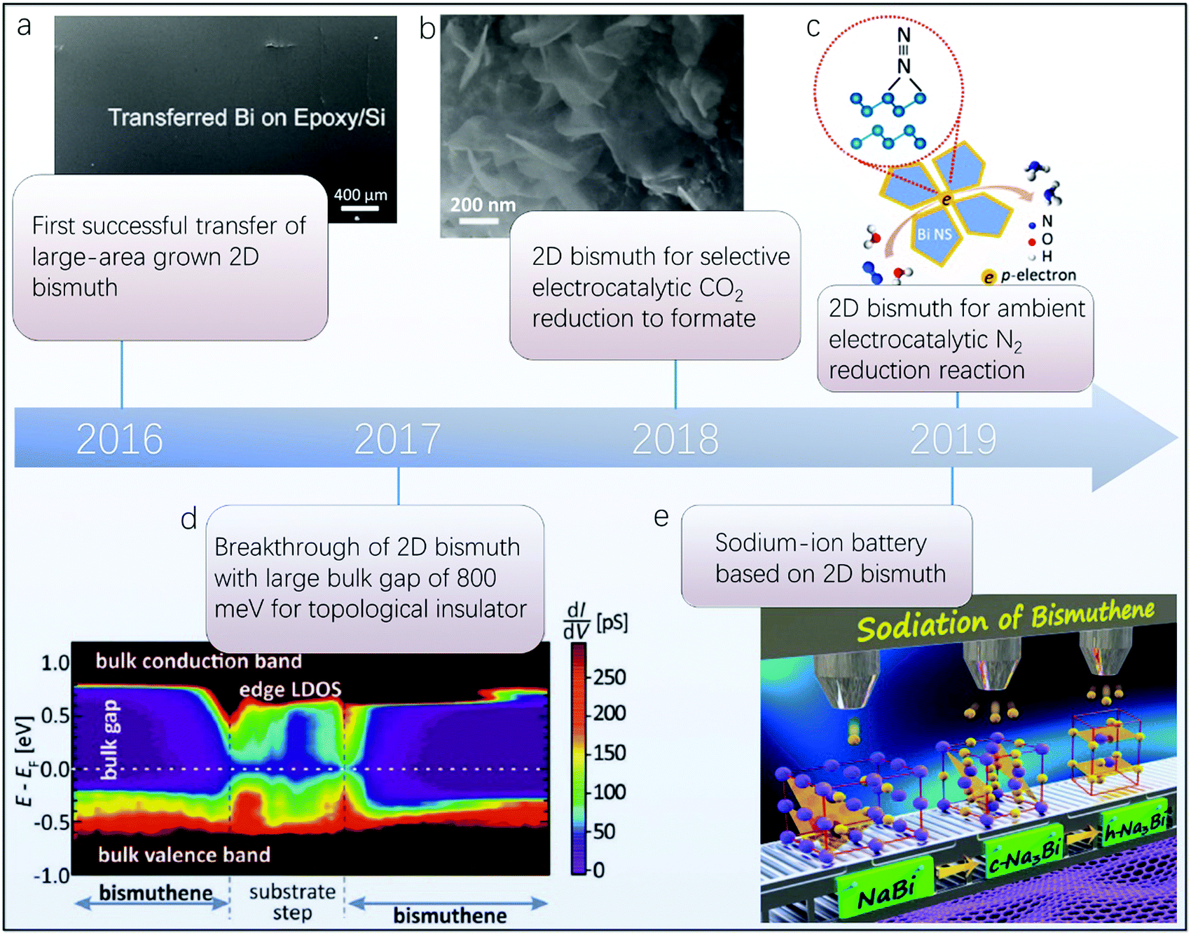 | ||
| Fig. 1 Timeline of recent representative experimental achievements of 2D Bi. (a) Transfer of large-area grown 2D Bi, demonstrating its potential for practical applications after growth via top-down and bottom-up methods (reproduced from ref. 60 with permission from the American Chemical Society, copyright 2016).60 (b) Application of 2D Bi for selective electrocatalytic CO2 reduction (reproduced from ref. 61 with permission from Nature Publishing Group, copyright 2018).61 (c) 2D Bi used for ambient electrocatalytic N2 reduction (reproduced from ref. 62 with permission from the American Chemical Society, copyright 2019).62 (d) Largest experimentally determined bulk gap from a topological insulator based on 2D Bi (reproduced from ref. 55 with permission from Science, copyright 2017).55 (e) 2D Bi implemented in sodium-ion battery applications (reproduced from ref. 63 with permission from the American Chemical Society, copyright 2019).63 | ||
In this review, firstly we will present an overview of the intrinsic properties of 2D Bi, such as the structure and thermodynamic stability, as well as insights into its air stability and electronic properties. We then thoroughly explore a multitude of fabrication techniques of 2D Bi. Afterwards, we proceed with experimental work on 2D Bi in energy-related applications, with perspectives on how to further develop more practical applications. Besides, it should be noted that the definition of “2D Bi” here not only refers to a single layer of bismuthene, but also includes other few-layer Bi and nanosheets with mesopores, as long as the lateral size of the 2D Bi is much larger than the sheet thickness.
2. Basics of 2D bismuth
The fundamental properties for practical applications of 2D Bi are directly determined by its structure stability, thermodynamic stability and electronic as well as spintronic characteristics. Moreover, the air-stability and non-toxicity of 2D Bi are also of great importance in opening appealing routes for practical applications.2.1. Structure and thermodynamic stability
Theoretically, based on DFT computations at the level expressed by the PBE functional, the binding energy calculations for all possible group VA monolayer configurations have been studied. Among them, three phases of bismuthene, i.e., α-, β- and ξ-phases, possess similar lowest average binding energy.56 We focus on two representative α-, β-phase bismuthene, because they have been experimentally obtained, which is in agreement with the theoretically-predicted energetic stability. Before that we have to agree on one manner to label these two bismuthene allotropes, since the indexing system varies in the literature.56,86–88Fig. 2a demonstrates the top and side views of β-phase bismuthene, which exhibits a buckled rhombohedral structure. It was first called the distorted A7 phase as early as in 1997,89 and we will call this phase structure Bi(111) in the rest of this review. Likewise, the top and side views of α-phase bismuthene are illustrated in Fig. 2b, which shows a puckered black-phosphorus-like structure. This phase of bismuthene was sometimes called the pseudocubic 012-oriented allotrope, also the A17 phase,90 and we will name it Bi(110) in the following discussion. It should be noted that these two allotropes of bismuthene, as a single layer, are composed of atoms at two different heights, resulting in the somehow confusing terminology “bilayer”, as demonstrated in the corresponding side views in Fig. 2.91 | ||
| Fig. 2 (a) Top and side views of Bi(111), which exhibit a buckled honeycomb structure. (b) Top and side views of Bi(110), which exhibit a puckered black-phosphorus style allotrope. | ||
Bi(110) has been investigated by combining experimental studies and first-principles calculations, in which non-trivial 2D topological insulator phases in Bi(110) films grown on Si(111) and highly oriented pyrolytic graphite (HOPG) were reported with a large bulk bandgap for possible topological properties at room temperature.92 Later, ultrathin bismuthene films were experimentally obtained on a TMD 1T-TaS2, which exhibits a structural transition to Bi(110) for ultrathin film thickness.93 Moreover, the energetically stable Bi(111) films were also experimentally grown on a NbSe2 superconducting substrate, and the detected superconductivity on different layers of the film along with the pairing potential demonstrates that the topological edge state can coexist with superconductivity.94 Apart from the energetically stable Bi(110) and Bi(111), a superstructure of bismuthene atoms in the honeycomb configuration on a SiC(0001) substrate has been realized.55 This fully planar bismuthene layer is also energetically favorable,95 exhibiting a lattice constant of 5.35 Å, considerably larger than that of Bi(111).
Further studies were performed to confirm the thermodynamic stability of bismuthene for practical application. The phonon spectra of both Bi(110) and Bi(111) have been calculated, which can be regarded as the criterion to judge the dynamic stability.96–98 No appreciable imaginary phonon modes were observed for bismuthene, suggesting its good dynamic stability.56 First-principles phonon and finite temperature molecular dynamics calculations including SOC demonstrated that the free-standing bismuthene is stable above room temperature. The ab initio molecular dynamics calculations were carried out from 300 K to 1000 K to clarify a certain elevated temperature (T = 700 K) at which the instability occurs due to thermal excitations.99
2.2. Air-stability and electronic properties
A robust high-performance 2D Bi-based device cannot be ensured solely by the aforementioned stability of the material structure and thermodynamics. In addition, poor air stability can also hinder the intrinsically high-performance device from being applied in practical implementations. Taking 2D black phosphorus for instance, its rapid degradation under ambient conditions is well-known, which could be due to a pathway of oxidation and subsequent exothermic reaction with moisture.100–104 In comparison, the best air-stability of 2D Bi among group VA materials has been experimentally demonstrated. Raman spectroscopy studies of freshly synthesized Bi(111) and the same sample after a 35 day aging period were carried out, and all peaks in the Raman spectra exhibited good consistency before and after the aging period.84 The unchanged surface roughness of the Bi(111) measured by atomic force microscopy (AFM) before and after the 35 day aging period assisted in confirming its good air-stability. Absorption spectral measurements and energy dispersive spectroscopy analysis were also performed to demonstrate that the Bi(111) sample can remain unchanged after the 35 day aging period.84 However, systematic investigations on the underlying physics of the good air-stability of 2D Bi are still rare in the literature.105 Further studies on 2D Bi in this aspect can combine experimental work with theoretical validations involving interactions with oxygen and defects related to water or other polar molecules.106 In addition, the gap between the conduction band and the vacuum level determines the electron affinity, and a lower value of electron affinity often suggests a more facile escape of electrons from the material atoms, corresponding to inferior air-stability.107,108 The electron affinity increases sequentially from phosphorene and arsenene to antimonene and bismuthene, as exemplified from energy levels of group VA monolayers with a (111) structure in Fig. 3a. This increasing trend of electron affinity with increasing atomic number could be another indication of gradually enhanced air-stability from phosphorene to bismuthene in the group VA column, which can in this regard qualitatively confirm the good air-stability of 2D Bi.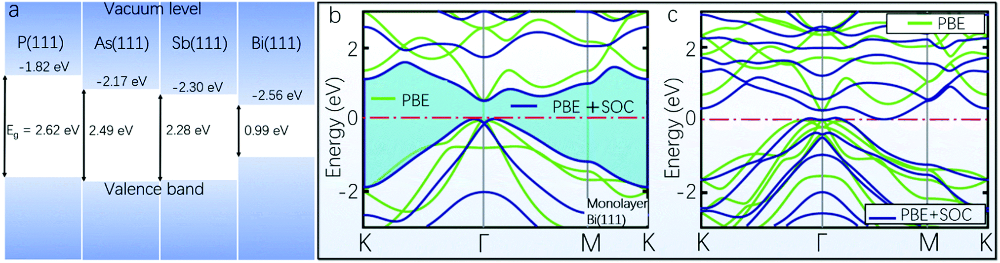 | ||
| Fig. 3 (a) Schematic illustration of the energy levels of group VA monolayers with the (111) phase, calculated at the HSE06 level of theory. (b) Electronic energy band structure of free-standing monolayer Bi(111) with a shaded gap between the valence and conduction bands, calculated by PBE (green lines) and PBE + SOC (blue lines).99 (c) Electronic energy band structure of two monolayers of Bi(111) with minimum energy stacking sequence (reproduced from ref. 99 with permission from the American Physical Society, copyright 2016).99 | ||
Regarding the electronic properties of bismuthene, we should begin with a brief discussion of SOC, because it has profound implications in heavy-atom 2D materials and is crucial in determining bismuthene band gaps. SOC equates the coupling between the effective magnetic field and the electron spin to the coupling between the electron momentum and the electron spin, which provides an indirect method to control electron spin.109 Rashba coupling is one type of SOC for possible control of spin states without a magnetic field, in which the spin–orbital interaction can lift the spin degeneracy owing to structural inversion asymmetry.110–112 Since SOC is relatively strong in bismuthene owing to the large atomic number of bismuth, the electronic band gaps can be significantly influenced by SOC in the DFT calculations. Taking 2D Bi in (111)-orientation as an example, calculations using the Perdew–Burke–Ernzerhof (PBE) functional without SOC predict a direct band gap of ∼0.55 eV for the optimized structure of Bi(111), as shown in Fig. 3b. In comparison, when SOC is included in the calculations, the degenerate bands at the top of the valence band exhibit a Rashba-type splitting (i.e., a Mexican-hat-like band splitting which is typical for Rashba SOC in 2D electron gas systems with structural inversion asymmetry), resulting in an indirect band gap of ∼0.51 eV,99 which are in agreement with previous theoretical studies.113,114
It bears mentioning that the above-calculated band gaps are usually underestimated solely using PBE functional, so the screened hybrid functional method at the HSE06 level can be used to correct the PBE values, leading to a direct band gap of ∼0.80 eV for a single layer of Bi(111). In addition, the consideration of SOC using HSE corrections results in a decreased band gap of ∼0.32 eV.99 A parallel study reported a direct band gap of ∼0.99 eV for single layer Bi(111), also derived from DFT computations at the HSE06 level without consideration of SOC, as provided in Fig. 3a.56,87 The discrepancy between −0.99 eV and ∼0.80 eV in the aforementioned two theoretical predictions could result from the slight difference in the input optimal lattice parameters in the two studies, and the implementation of different calculation packages (CASTEP and VASP, respectively) might be another reason for the approximately 20% deviation.56,99
After discussing the electronic properties of single layer Bi(111), we now turn to the energy levels of two layers of Bi(111) calculated using the PBE functional, in an attempt to further reveal the SOC effect and to demonstrate the semiconductor-to-semimetal transition with increasing layers of 2D Bi. As shown in Fig. 3c, the two layers of Bi(111) exhibit a band gap of ∼0.23 eV, which changes to a metal if SOC is taken into consideration.99 This suggests that the absence of the interlayer interaction might result in opening a band gap in single layer Bi(111).
The air-stability and electronic properties of bismuthene layers should be further explored and confirmed by more systematic experimental investigations. Fortunately, the fabrication techniques to obtain 2D Bi have been significantly improved in the past several years (see Section 3), which can lead to more reliable experimental work to, in turn, compare with theoretical predictions. For instance, recently bottom-up grown centimeter-scale 2D Bi thin films were experimentally integrated into FETs and demonstrated p-type transport characteristics, and the corresponding thickness-dependent band gaps were also observed from optical absorption measurements.115 This can be regarded as a good support for theoretical studies of 2D Bi FETs predicted by first-principles energy band calculations and quantum transport simulations.71
2.3. Cytotoxicity
The materials used in commercial applications should not be toxic, mutagenic or carcinogenic. However, many substances in commercial products may not be completely friendly to human health, and their toxicity should be systematically investigated and limited within a reasonable level. For example, even though cadmium-containing light-emitting diode down-conversion layers have received huge success in the display industry,116 the health impact of cadmium-containing quantum dots has raised concerns with toxicologists for a long time, and cadmium-free quantum dots are under urgent investigation to avoid potential risk to human health.117,118 In comparison, little effort has been devoted to determining the toxicity of bismuthene layers. Recently, Chia et al. investigated the toxicological effects of group VA nanosheets with various concentrations of test materials and adenocarcinoma human lung epithelial A549 cells.85 It was found that the mild cytotoxicity induced by Bi thin layers can be neglected, whereas arsenic and antimony thin layers are considered to be highly toxic and moderately toxic, respectively. Also, 2D Bi was found to be less toxic compared with the corresponding bismuthene(III) oxide salts.85 Therefore, it can be concluded that paranoid-like concern might not be necessary regarding the cytotoxicity of 2D Bi-based devices, but more investigations are still needed to elucidate the underlying mechanisms of the biological responses towards 2D Bi.3. Fabrication methods
The difficulty of efficiently obtaining high-quality 2D Bi is a significant roadblock to experimentally explore 2D Bi-based devices in energy sciences. However, a variety of fabrication methods have been gradually improved in the past several years to obtain 2D Bi, which can be generally categorized as top-down methods, bottom-up methods and wet chemical methods. Among them, we can regard top-down and bottom-up methods as direct fabrication techniques, because the resulting 2D Bi are directly obtained from bulk bismuth crystals either via top-down exfoliation or bottom-up formation. In comparison, the wet chemical method can be treated as an in-direct fabrication technique, since the staring materials are usually bismuth-containing compounds from which we can get 2D Bi through chemical reaction procedures.3.1. Top-down methods
Regarding top-down methods, bulk bismuth crystals are treated as the starting materials for the subsequent exfoliation of layered 2D Bi. We will mainly focus on two types of top-down fabrication techniques, namely, liquid exfoliation and hot-pressing methods, though other top-down fabrication methods are also available, such as magnetron sputtering119–121 and mechanical cleavage after Bridgman synthesis.122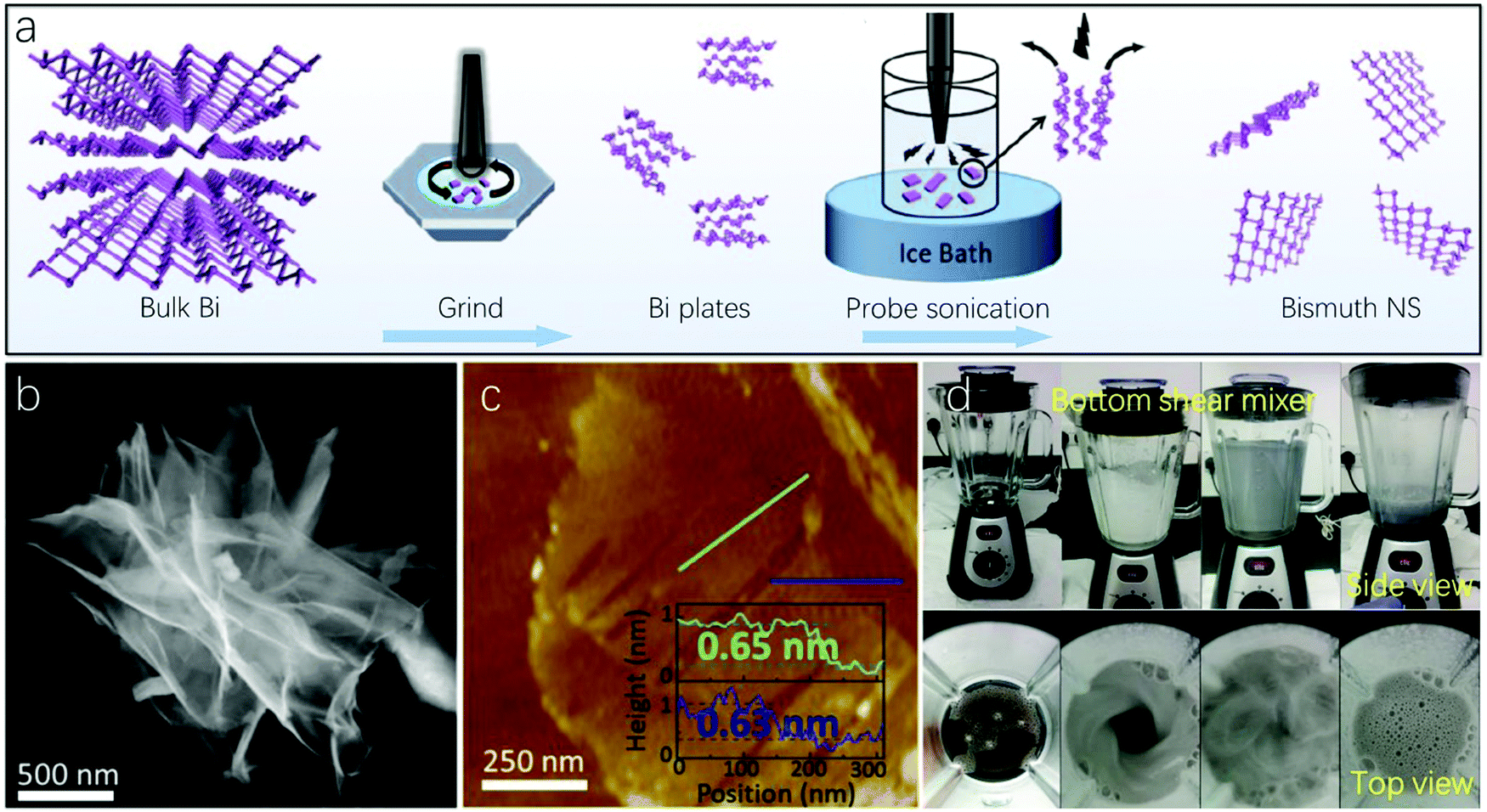 | ||
| Fig. 4 Top-down methods to fabricate 2D Bi. (a) Schematic illustration of 2D Bi preparation by probe sonication liquid exfoliation. (b and c) Demonstrate the TEM and AFM images of 2D Bi prepared by sonication liquid exfoliation, respectively (reproduced from ref. 63 with permission from the American Chemical Society, copyright 2019).63 (d) Photograph of bottom shear mixing in the shear exfoliation process (reproduced from ref. 20 with permission from Wiley, copyright 2019).20 | ||
Aqueous shear exfoliation has recently been applied to fabricate bismuthene thin layers.20 The Bi bulk crystals were subjected to shear dispersion and exfoliated in aqueous surfactant sodium cholate for 2 hours alternating between bottom and top mixers with kitchen blenders. Fig. 4d demonstrates the photograph of the bottom shear mixer with both side and top views. The liquid-phase shear, turbulence and collisions can lead to a lateral force for lubricating exfoliation of the starting bismuth crystal. The corresponding HRTEM image in this work demonstrates a perfect inter-distance of the lattice fringe. This scalable and simple aqueous shear exfoliation method was also used to fabricate 2D Bi for other applications, such as cytotoxicity investigation and biosensing.85,131
3.2. Bottom-up methods
Bottom-up fabrication methods refer to the direct growth of 2D Bi on a specific substrate from an evaporation source containing bulk Bi crystals, which can be generally classified as physical vapor deposition (PVD) and pulsed laser deposition (PLD).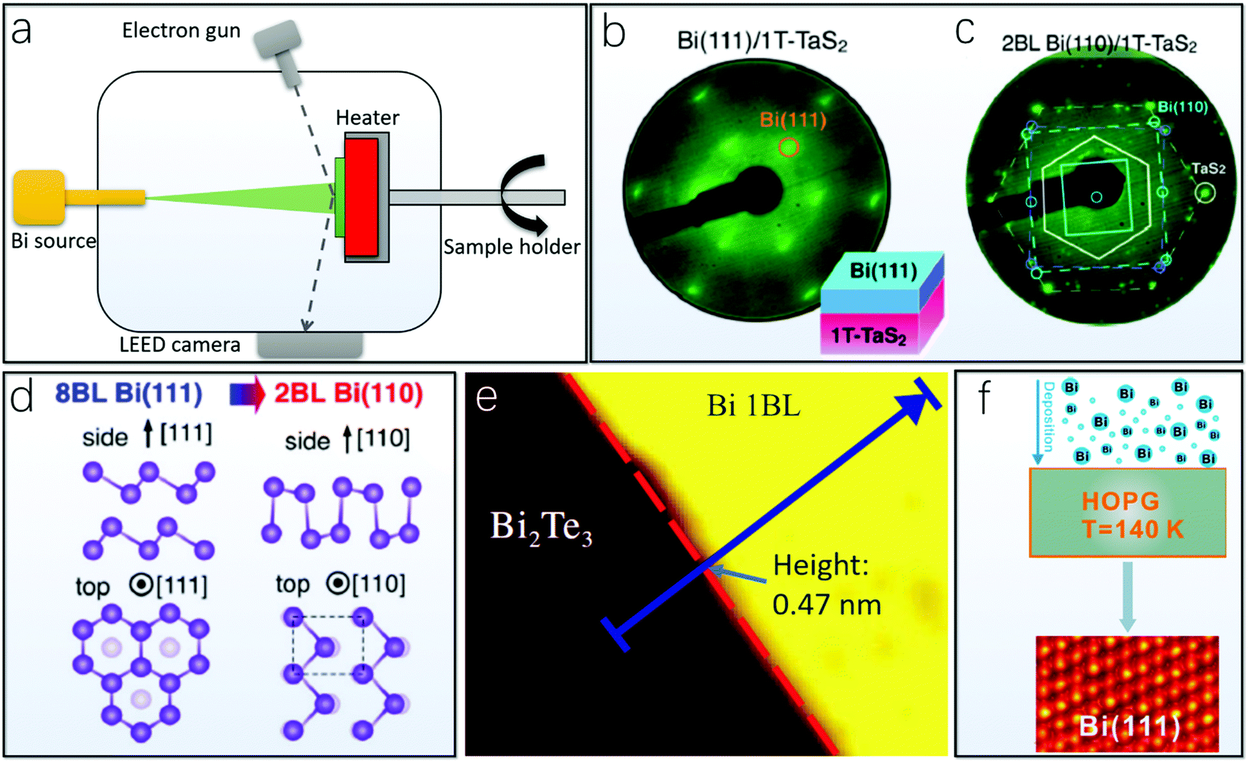 | ||
| Fig. 5 Molecular beam epitaxy (MBE) for fabricating Bi(110) and Bi(111). (a) Schematic illustration of the MBE setup. (b) LEED pattern of a relatively thick layer of Bi(111) deposited on 1T-TaS2.93 (c) LEED pattern of 2 bilayers of Bi(110) on 1T-TaS2. (d) Schematic depiction of the structure transition of Bi(111) and Bi(110) on 1T-TaS2 (b–d, reproduced from ref. 93 with permission from the American Chemical Society, copyright 2018).93 (e) Direct growth of a single bilayer of Bi(111) on Bi2Te3 (reproduced from ref. 135 with permission from the American Physical Society, copyright 2012) (ref. 135). (f) Direct deposition of a single bilayer of Bi(111) on HOPG at a low temperature of 140 K (reproduced from ref. 141 with permission from the American Chemical Society, copyright 2015) (ref. 141). | ||
Via MBE methods, the initial deposition of Bi layers on most substrates tends to result in Bi(110) ultrathin layers, which can be followed by Bi(111) layers upon additional deposition thickness. For instance, Bi thin films have been found to undergo this structural transition from (111) to (110) upon reducing the Bi film thickness using 1T-TaS2 as the substrate.93 First, the Bi thin film was deposited at 370 K via the MBE technique on the freshly cleaved shiny mirror-like surface of 1T-TaS2 under UHV conditions. The LEED pattern demonstrated a drastic change accompanied by new 1 × 1 spots from bismuthene layers and the disappearance of 1T-TaS2 spots. As shown in Fig. 5b, the overall six-fold symmetry of the LEED pattern suggests the (111) orientation of the bismuthene layers. In situ angle-resolved photoemission spectroscopy (ARPES) and AFM measurements were also used in that study to confirm the (111) orientation of the bismuthene layers. In contrast, when an ultrathin (2 bilayer) Bi film was deposited on the 1T-TaS2 substrate, both of the corresponding second-derivative ARPES intensities of the 2 bilayers measured along the ΓM cut of the TaS2 Brillouin zone and the AFM image with several needle-like Bi growing features can indicate a (110) orientation of the ultrathin bismuthene layers. The LEED pattern in Fig. 5c shows that the 2 bilayer Bi(110) film is composed of three domains rotated by 120° from each other, which is in agreement with the expectation from the symmetry of the Bi(110) overlayer and the 1T-TaS2 substrate. The schematic illustration of the structural transition from (111) to (110) is presented in Fig. 5d, and it is speculated that the Bi(110) layers are coupled to the 1T-TaS2 substrate, whereas the thicker Bi(111) layers exhibit similar triangular islands irrespective of the type of substrate surfaces.
The underlying mechanism of this structural transition of bismuthene layers during the MBE process was first experimentally elucidated by Nagao et al. as early as in 2005.133 They deposited bismuthene layers from an alumina-coated tungsten basket onto a Si(111) substrate under <1 × 10⁻¹⁰ torr at room temperature, and the bismuthene layers were in situ characterized by a combination of reflection high-EED (RHEED) and scanning tunneling microscopy (STM). It was found that the 2D Bi film growth was initiated with the formation of (110) oriented bismuthene which was followed by a structural transition into the (111) phase at thicker thickness. This might be because that the surface Bi atoms lose only one second-nearest bond at ultrathin thickness, whereas the surface bismuth atoms lose three second-nearest bonds at thicker thickness. The surface effect becomes less dominant with swift cohesive energy approaching the bulk value as the thickness increases. In comparison, the cohesive energy of Bi(110) cannot approach the bulk value at larger thickness because of the presence of strain owing to its puckered structure, resulting in stable Bi(110) solely at ultrathin thickness.133
However, based on the above discussion, it is not necessary for a pessimistic view that ultrathin Bi(111) cannot be directly grown without the initial formation of Bi(110) layers, because so far at least two approaches are available to directly obtain single layer Bi(111) via the MBE technique. The first approach is to couple Bi(111) with a more suitable substrate, such as Bi2Te3, Bi2Se3 and Sb2Te3, which possess a similar layered structure and small in-plane lattice mismatch. Hirahara et al. used the substrate Bi2Te3 and succeeded in growing a single bilayer Bi(111) for the first time, mainly because of the nearly the same lattice constant of Bi and the Bi2Te3 substrate.134 Later, Yang et al. studied the spatial and energy distribution of topological edge states in single layer Bi(111) with Bi2Te3 as the deposition substrate.135 The topography of the Bi/Bi2Te3 step is illustrated in Fig. 5e. They also performed real-space scanning tunneling spectroscopy (STS) with the corresponding bias voltage dependence of the edge states (in the energy range +136 mV to +370 mV) measured perpendicular to the step edge. The experimental result clearly demonstrates the existence of nontrivial topological edge states of single bilayer Bi(111), also showing the reliability of the bismuthene growth via the MBE method with an appropriate substrate. The growth mechanism and interface structure between single bilayer Bi(111) and Bi2Te3 was further investigated via a combination of STS, low temperature STM as well as local work function measurements.136 Temperature-dependent growth modes were proposed, i.e., the Bi(111) growth proceeds via a quasi-bilayer-by-bilayer mode at room temperature, and the growth at elevated temperature (300–450 K) proceeds via a step-flow mode. Moreover, Bi atoms can evaporate from the Bi2Te3 surface when the substrate temperature is higher than 450 K, whereas Bi atoms cluster with a typical size of ∼3 nm below approximately 150 K.136
This appears to be contradictory to the subsequently introduced second approach to directly obtain single layer Bi(111), i.e., low-temperature (140 K) deposition on HOPG with the aim of tuning the bismuthene growth kinetics. The inertness of the graphite surface together with its atomic smoothness makes HOPG an ideal substrate for nanostructure growth, on which Bi atoms often tend to form (110) oriented ultrathin films rather than (111) orientation owing to the better stability of Bi(110) in the ultrathin film regime.92,137–140 However, when the bismuthene layers are deposited on a freshly-cleaved HOPG surface at a low temperature of 140 K (Fig. 5f), the growth orientation can be directly altered to the (111) facet, allowing a potential single constituent topological material for topologically based spintronic devices.141 At this low deposition temperature, the Bi atoms are rather mobile on the HOPG terraces without evidenced interaction between the bismuthene layer and the underlying substrate, which was further confirmed by the core level measurements of Bi 4f and C 1s.
Therefore, up to now it can be concluded as follows: even though bismuthene deposited via the MBE technique generally tends to grow with (110) orientation at ultrathin coverage below a critical thickness and is able to transform into (111) orientation above this critical thickness, this thickness can be tuned to some extent by a combination of substrate and temperature variations. This substrate- and temperature-dependent critical thickness can provide a wide variety of solutions to obtain bismuthene with different phases targeting diverse applications. It should be noted that Bi(110) and Bi(111) have also been investigated based on a variety of other substrates, such as Au(111),142 Si(001)143 and Al2O3,86 which further suggests the potential to develop more improved fabrication methods for 2D Bi-integrated devices.
Apart from the above-mentioned bismuthene with (110) and (111) orientation, bismuthene layers with other different configurations were also obtained on various substrates via the MBE technique. For instance, a monolayer Bi physisorbed on top of Bi(110) with an underlying HOPG substrate was found to possess rectangular symmetry similar to that of the Bi(110) structure, but with a substantially contracted surface unit cell, as shown in Fig. 6a.91 This single layer Bi with rectangular symmetry tends to grow from the defective spots of Bi(110) stripes, which might start with pinning of the diffusing Bi atoms by a kink in the stripe with subsequent monolayer Bi nucleation. Moreover, Reis et al. recently epitaxially deposited fully-planar monolayer bismuthene with a 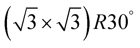 superstructure in a honeycomb geometry on a hydrogen-etched SiC(0001) substrate (Fig. 6b).55 The lattice constant (5.35 Å) of this fully-planar bismuthene is significantly larger compared with that of Bi(111). A nontrivial quantum spin Hall phase with 800 meV bulk gap was experimentally determined from this fully-planar single layer bismuthene, demonstrating the critical role of the SiC(0001) substrate for controlling the relevant orbitals in 2D quantum spin Hall insulators.55,144 Furthermore, another new growth pattern for single layer bismuthene epitaxially grown on a NbSe2 substrate was reported, in which the initial growth of Bi atoms can lead to a strongly bonded commensurate layer, resulting in a compressively strained ripple-like 2D triangular lattice, as illustrated in Fig. 6c.145 The representative PVD-fabricated 2D Bi layers deposited on different substrates are provided in Table 1.
 | ||
| Fig. 6 MBE-fabricated ultrathin bismuthene layer with phase different from (110) and (111) orientations. (a) Bi(110)-like monolayer bismuthene (MBi) with a contracted surface unit cell on a HOPG substrate in top and side views (reproduced from ref. 91 with permission from the American Physical Society, copyright 2017).91 (b) Fully-planar monolayer bismuthene epitaxially grown on SiC(0001) (reproduced from ref. 55 with permission from Science, copyright 2017).55 (c) Monolayer bismuthene with a ripple-like 2D triangular lattice epitaxially grown on a NbSe2 substrate (reproduced from ref. 145 with permission from Science, copyright 2018).145 | ||
| 2D Bi | Substrate | Layers or thickness | Ref. |
|---|---|---|---|
| Bi(110) | 1T-TaS2 | ∼1 monolayer | 93 |
| Si(111) | ∼1 monolayer | 133 | |
| HOPG | Several monolayers | 92 and 137–140 | |
| Au(111) | Several monolayers | 142 | |
| Al2O3 | Tens of nanometers | 86 | |
| Bi(111) | 1T-TaS2 | ∼4 monolayers | 93 |
| Si(111) | >7 monolayer | 133 | |
| Bi2Te3 | ∼1 monolayer | 134–136 | |
| HOPG | ∼1 monolayer | 141 | |
| Si(001) | ∼6 nm | 143 | |
| Al2O3 | Tens of nanometers | 86 | |
| Others | SiC(0001) | Fully-planar monolayer | 55 |
| NbSe2 | Monolayer | 145 | |
For clarity, it has to be mentioned that another bottom-up method, i.e., chemical vapor deposition (CVD), is not available for fabrication of 2D Bi. CVD involves decomposition and subsequent adsorption of precursors, and this high-yield fabrication method has been widely applied to obtain multi-elemental 2D materials, such as boron nitride,146–148 perovskites,149,150 and TMD nanosheets on arbitrary substrates.151,152 To obtain mono-elemental 2D materials, taking graphene as an example, a hydrocarbon gas flow for carbon adsorption is needed.153–155 In comparison, no gas flow containing Bi atoms is available for CVD-grown 2D Bi. However, the CVD setup can be used to fabricate 2D Bi, which should be regarded as another type of thermal evaporation method.156 Last but not least, a double cantilever beam fracture technique was for the first time successfully applied to dry-transfer large-area 2D Bi grown on Si(111) to epoxy-coated silicon strips, demonstrating the potential of 2D-Bi for practical applications after growth via bottom-up methods.60
3.3. Wet chemical methods
If we do not consider the detailed chemical compositions and material transformation procedures, the wet chemical method can be roughly regarded as a liquid-phase equivalent of CVD, in which a Bi-based compound is used as the starting material to obtain 2D Bi through chemical reactions. Inspired by the synthesis of Bi nanotubes,163 Kumar et al. extended the low-temperature template-free synthesis method to fabricate high-yield ultrathin Bi layers, in which Bi nitrate pentahydrate was mixed with DI water, ethylene glycol and hydrazine hydrate in a volume ratio of 6:3:1 with subsequent vigorous stirring and washing.164 Alternatively, Bi nanoflakes with a 2D structure were synthesized on a Ni foam through a replacement reaction, and obtained by a slow reduction of Bi3+ by Ni foam.165
Pulse current electrodeposition is an alternative way to fabricate 2D Bi. Kim et al. mixed Bi nitrate pentahydrate (Bi(NO)3)3·5H2O and hydrochloric acid with DI water, and pulse current electrodeposition of 2D Bi was carried out in a three-electrode system.76 Compared with direct-current electrodeposition,166,167 pulse current electrodeposition can result in more uniform films, because the ions diffuse from the solution to the working electrode surface, thereby lowering the concentration gradient during the next pulse-on-time. The Bi nanoflakes with sharp edges and corner sites demonstrated a maximum faradaic efficiency of nearly 100%.76
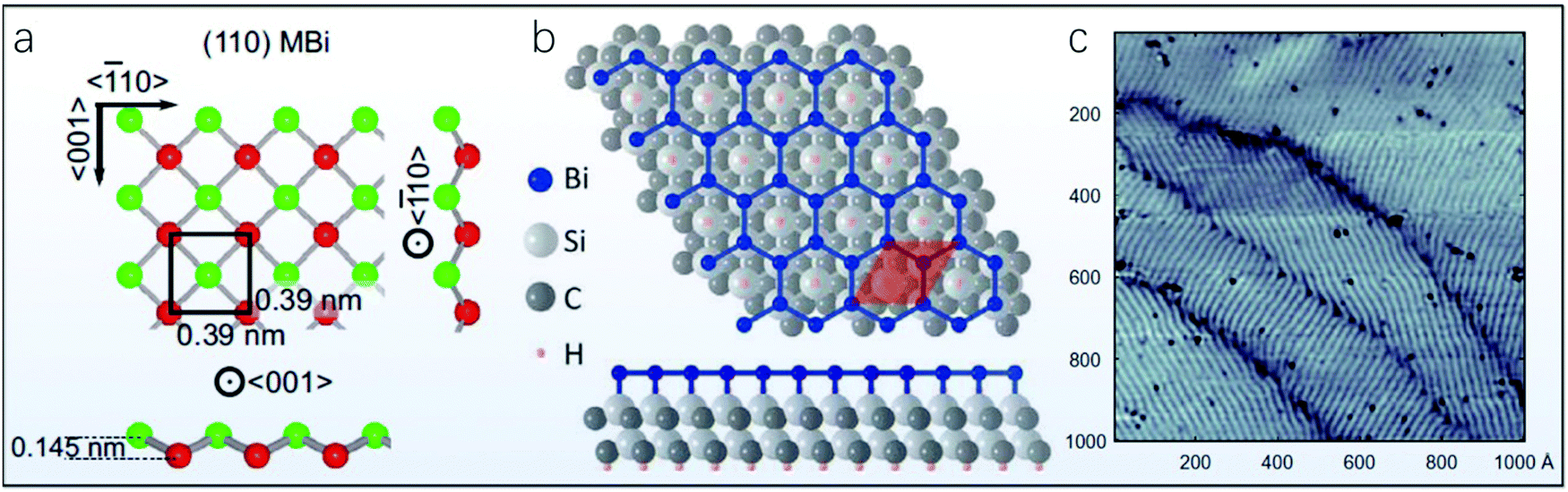
A Bi-based compound in an appropriate solution can also be treated as a template to obtain 2D Bi. For example, inspired by a recent study that reported in situ formation of CO2 reduction reaction (CO2RR) catalysts using operando electro-redeposition,168 Sargent et al. employed Bi oxyhalide (BiOBr in this case) as a template to derive 2D Bi-based catalysts.169 As shown in Fig. 7a, Bi oxyhalides are separated by negatively charged halogens, and upon electroreduction ultrathin Bi layers can be obtained after dynamically removing the halogen layers. The resultant CO2RR selectivity is over 90% faradaic efficiency with a stable current density of up to 200 mA cm−2. In the meantime, mesoporous Bi nanosheets with a large surface area were prepared by cathodic transformation of atomic-thick Bi oxycarbonate (Bi2O2CO3) nanosheets with an enhanced CO2RR selectivity of up to 100% faradaic efficiency.80
 | ||
| Fig. 7 Wet chemical methods to fabricate 2D Bi. (a) Atomic structure of BiOBr and the BiOBr-templated Bi catalyst after electroreduction. (b and c) Provide SEM image of BiOI nanosheets and topotactically reduced Bi nanosheets, respectively (reproduced from ref. 61 with permission from Nature Publishing Group, copyright 2018).61 | ||
In comparison, another Bi-based compound template, i.e., Bi oxyiodide (BiOI), consists of hierarchical micro-flowers that are assembled from very thin nanosheets oriented to different directions, as demonstrated in Fig. 7b. These BiOI nanosheets are synthesized by reacting Bi(NO3)3 and KI at 160 °C for 2 hours, and the obtained BiOI nanosheets exhibit a layered tetragonal structure where [Bi2O2] slabs are sandwiched between anionic iodide layers.61 After the in situ topotactic transformation of BiOI nanosheets in a cathodic electrochemical environment, the resulting Bi layers retain the 2D morphology with some of them curved and folded (Fig. 7c), which enables high-performance CO2 reduction to formate with a faradaic efficiency of over 90%. In addition, 2D mosaic Bi nanosheets were recently fabricated via the in situ electrochemical reduction of BiOI nanosheets for N2RR instead of CO2RR, and in this scenario nanoflakes with size less than 10 nm can be observed scattered in the matrix of the Bi nanosheets, resulting in a mosaic morphology.62
4. Applications in energy sciences
After thoroughly reviewing the various fabrication methods, in this section we will discuss the experimental implementations of 2D Bi in energy sciences, namely, energy saving via energy-dissipationless topological insulators, energy storage via Bi-integrated batteries, as well as energy conversion applications such as CO2 reduction and N2 fixation. Besides, the readers are encouraged to refer to several comprehensive reviews covering the recent development for all the group VA 2D materials,1,54,87,170–172 along with several review articles regarding other energy-related applications for a more comprehensive interpretation, such as photonics,84 thermoelectricity and optoelectronics,173 and electrochemistry from a theoretical perspective.1744.1. Energy saving: topological insulator (TI)
In physics, TI refers to a special type of material, which is insulating in the bulk but has metallic (gapless) states located at the surface (for 3D TI) or the edge (for 2D TI) of the material.175 The existence of the boundary states is robust against any perturbations as long as they do not close the bulk bandgap. The mathematical description for such a state relies on the concept of topology: the topological character of the band structure is preserved under any smooth deformations as long as the bandgap is maintained, just like the number of holes (a topological character for the 2D closed manifold) is preserved during the smooth transformation from a donut to a coffee cup.176 In a broad sense, the term “TI” can also include nontrivial insulators in magnetic systems, such as the quantum anomalous Hall insulator. In the following discussion relevant to 2D Bi, we restrict the term to its original scope, namely, for nontrivial insulators in time-reversal-invariant systems.One unique property of the boundary states of TI is that the spin direction is tied with the momentum, and for states at opposite momenta, their spin parts must be orthogonal, as required by the time reversal symmetry. It follows that the electron backscattering, which is the main contribution to resistance and hence energy dissipation, can be strongly suppressed for transport through these topological states.177,178 Moreover, since the boundary states are spin polarized, they naturally offer a promising platform for energy-saving semiconductor spintronics. Regarding 3D TIs, the contribution of bulk electrons from crystal imperfection often interferes with the surface electron transport, and although the backscattering is suppressed, the small-angle scattering among the 2D surface states is still allowed.179,180 In comparison, the 2D TI has the advantage of being more easily controlled in experiment with high quality, and its topological boundary states are 1D spin-helical edge channels, for which any elastic scattering from non-magnetic disorders is in principle strictly prohibited. Fig. 8a demonstrates the schematic illustration of the 1D helical edge state of a 2D TI with counter-propagation of opposite spin states.
 | ||
| Fig. 8 (a) Schematic illustration of the counter-propagation of opposite spin states in a 2D TI. (b) Energy dispersion of the edge states in a 2D TI. | ||
A TI material typically requires a large SOC with an inverted band ordering. To be specific, for common semiconductor materials, the conduction and valence bands are formed from s-orbital and p-orbital electrons, respectively. In comparison, for TIs with heavy elements, the SOC can be adequately large so that the s-orbital and p-orbital bands are pulled to be inverted. In the energy spectrum, the pair of helical edge states appear in the bulk bandgap, dispersing from the valence band to the conduction band with a cross at k = 0, as required by the time-reversal symmetry (Fig. 8b).181–183
The investigations on TI materials started with a number of theoretical predictions,184–186 and the type III semiconductor CdTe/HgTe/CdTe quantum wells, in which a thin layer of HgTe was sandwiched by CdTe, were experimentally demonstrated as the first example.187 When the thickness of HgTe is above a critical value of 6.3 nm, the samples exhibit inverted bands. However, the bulk gap (∼10 meV) of this material combination is so small that the TI phase can be only observed at a very low temperature (30 mK). The AlSb/InAs/GaSb/AlSb quantum wells are another experimentally confirmed 2D TI, in which the even smaller bulk gap (∼4 meV) results from the anti-crossing of the hole and electron bands at finite momentum.188,189 Apart from the tiny bulk gap of the above-mentioned quantum wells, the significant difficulty of the elaborate fabrication process is another drawback of such TI systems.
We then focus on mono-elemental 2D TIs, which mainly come from group IVA and group VA materials. In fact, graphene was the first theoretically predicted TI. However, the SOC in graphene is very weak because of the small atomic number of carbon.190 The experimental detection seems to be unrealistic because of the extremely small gap opened by SOC (on the scale of 10−3 meV).186,191 Later, it was predicted that the SOC-induced gap of silicene, i.e., 2D silicon with a buckled honeycomb structure, is about 1.55 meV, which can be further increased to 2.9 meV under strain, bringing more optimism in obtaining mono-elemental 2D TI at an experimentally accessible low temperature.192,193 The example shows that the SOC gap generally increases with increasing atomic number and can be enhanced by the buckling of the structure. Along this line of research, it was predicted that germanene is also a TI with a bandgap of about 23.9 meV, already higher than the liquid nitrogen temperature.37,192 A 2D tin film (known as stanene) was predicted to be a TI with a bulk gap of 300 meV.194 After the first successful MBE fabrication of stanene on the Bi2Te3 substrate,38 high-quality MBE-grown stanene on Cu(111) exhibiting an in-plane s–p band inversion and a SOC-induced bulk gap of ∼300 meV at the Γ point was recently experimentally confirmed.182 In addition, regarding antimonene, its theoretically predicted tunable large bulk gap in the range of 101–560 meV can also make it a promising candidate material for room-temperature TI with a quantum spin Hall effect.195
Even better than antimonene in terms of exploring TI, Bi has the largest atomic number in group VA (in fact the largest among all stable and nonradioactive elements), which endows bismuthene with strong SOC strength. Via the calculation of the helical edge states and demonstration of the nontriviality of the Z2 topological number, Murakami was the first to theoretically predict that 2D Bi can host a 2D TI state,196 which was followed by intensive theoretical investigations and experimental confirmations of its topological character.66,67,69,86,94,134–136,142,145,197–199
The 2D Bi used for TI investigations is usually fabricated via MBE methods, which can precisely control the ultrathin thickness of the targeted materials. In Section 3.2.1, we have discussed how to obtain (111)-, (110)-, as well as fully-planar bismuthene using MBE methods. Their TI properties are often characterized by three kinds of techniques, namely, ARPES, STM and STS. ARPES measurements have been widely used to detect the topological boundary states, and the first ARPES experiments were carried out by Hsieh et al. on the topological boundary states of a Bi1−xSbx alloy.200 In addition, STM and STS represent surface-sensitive techniques to probe the topological boundary states.
In the following we will discuss the representative experimental investigations on TI properties from (111)-, (110)-, and fully-planar bismuthene conducted by these three types of characterization techniques. Yang et al. have deposited 1-bilayer Bi(111) on the Bi2Te3 substrate, from which the edge states are observed in the vicinity of the Bi/Bi2Te3 step edge with a spatial distribution of several nanometers in real space using the combination of STM and STS measurements, as shown in Fig. 9a. The fact that the edge states lie directly inside of the 2D bulk gap demonstrates the existence of 1D topological in-gap edge states in the 1-bilayer Bi(111).135 Regarding ultrathin Bi(110), it has been theoretically predicted that Bi(110) prefers to adopt a bilayer stacking structure, and even-monolayer Bi(110) films are more stable compared with odd-monolayer films due to the easier saturation of dangling bonds for even-monolayer ones. Therefore, Lu et al. further calculated band structures of 2-monolayer (1-bilayer), 4-monolayer (2-bilayer) and 6-monolayer (3-bilayer) Bi(110), and they focused on 2-monolayer (Fig. 9b) and 4-monolayer bismuthene because of the metallic nature of 6-monolayer Bi(110).92 The spectra of both 2-monolayer and 4-monolayer Bi(110) grown on HOPG exhibit gap features associated with the bulk bands of 2-monolayer and 4-monolayer films. It bears mentioning that both the bulk and edge states can be accessed by STS measurement, which is unlike the quantum-well 2D TI. In addition, the band topology of ultrathin Bi(110) is sensitive to atomic buckling, which can be tuned by charge doping and variation of substrates.92 Interestingly, it was recently revealed that the buckling in the Bi(110) monolayer leads to an in-plane ferroelectricity (the first example of an elemental ferroelectric),201 so that the topological phase may also be tuned by an applied electric field.
 | ||
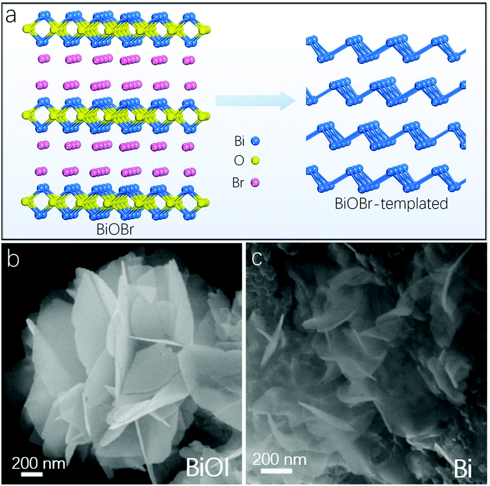
| Fig. 9 Characterization of Bi(111), Bi(110) and fully-planar bismuthene using ARPES, STM, and STS. (a) STS map of 1-bilayer Bi(111) on Bi2Te3 with the step edge marked by the red dashed line (reproduced from ref. 135 with permission from the American Physical Society, copyright 2012).135 (b) Shows the STS spectrum performed at 77 K from the edge to inside of terrace of 1-bilayer Bi(110) on the HOPG substrate. The dashed lines represent the gap size determined far away from the edges (reproduced from ref. 92 with permission from the American Chemical Society, copyright 2015).92 (c) Close-up of ARPES illustrating a valence band maximum at the K point with large SOC-induced splitting of the fully-planar bismuthene on SiC(0001), with the sketch in the top-right corner showing the orientation of the cut (black lines) in the momentum space of the surface Brillouin zone.55 (d) Differential conductivity of fully-planar bismuthene at different distances to the edge. The inset shows the STS measurement locations (color-coded dots relate to spectrum color) at the uphill substrate step causing the boundary (reproduced from ref. 55 with permission from Science, copyright 2017).55 | ||
The breakthrough work in terms of a room-temperature operated 2D TI was recently carried out by Reis et al., in which the combination of theoretical and experimental results based on a fully-planar bismuthene on SiC(0001) demonstrates an experimentally determined wide bulk gap of 800 meV, showing great potential to obtain a large gap TI in monolayer-substrate composites.55 A large band splitting of 0.43 eV was derived from the close-up of ARPES (Fig. 9c), which is the distinct Rashba characteristics of this system. Importantly, they excluded the existence of double layer bismuthene films and confirmed the realization of a single fully-planar bismuthene via a combination of ARPES measurement and DFT calculations. The bismuthene surface was covered by flakes with a typical diameter of 25 nm, and the flakes can be terminated by steps of the SiC substrate. Moreover, the differential tunneling conductivity curves shown in Fig. 9d can reflect the local density of states, and a large bulk gap of approximately 800 meV can be directly observed from the spectrum. The large 2D Bi bulk gap induced by the strong SOC and the effective coupling with the underlying substrate are also of vital importance for the manipulation of spins, which can pave the way towards the combination of spin transport and spin-to-charge conversion in 2D systems, if further coupled with other 2D materials with low intrinsic SOC for efficient spin transport.202–204
Apart from the aforementioned experimental achievements of 2D Bi for energy-dissipationless implementations, more innovative energy-related studies on 2D Bi might be inspired by the recent pioneering experimental work performed by Cao et al. on bilayer graphene, in which gate-tunable superconducting and correlated insulating phases can be further obtained by twisting the layers to a “magic angle” of 1.1°.205,206 It could be optimistically speculated that a magic angle might also be possible between two layers of closely packed 2D Bi if coupled with more advanced material fabrication and transfer techniques.
4.2. Energy storage: batteries
The intercalation-based lithium-ion battery is popular in the current energy storage market, and it might be replaced by the more appealing sodium-ion battery, which is based on much more low-cost and abundant sodium.207,208 Areal capacities with high mass loading are important for a sodium-ion battery in practical applications, which leads to the requirement of developing new electrode materials with high areal capacities.75,209–212 In this aspect, Bi is an intriguing anode candidate material due to its high theoretical volumetric capacity of approximately 3800 mA h cm−3 and favorable sodium alloy potential.54,63,75 The sodiation mechanism of Bi generally consists of two steps, namely, the intercalation and alloying process.213,214 The huge volume change during the intercalation and alloying reactions is the most severe problem hindering the development of this type of battery. In comparison, 2D Bi can provide much better reversibility owing to the enhanced gaps between the exfoliated nanosheets, leading to penetration of more sodium ions into the crystal structure without structure pulverization.54,171In order to explore the sodiation dynamics of the 2D Bi by a time-resolved process inside TEM, an all-solid nanosized sodium-ion battery is constructed, as shown in the schematic illustration in Fig. 10a.63 This nanosized battery is composed of a 2D Bi electrode dispersing on the carbon film-supported TEM grid, and a metal sodium counter electrode on a sharp tungsten probe, as well as a solid electrolyte of Na2O layer grown on the metal sodium surface. A piezo-positioner was used to drive the tungsten probe to make the contact of Na/Na2O with the 2D Bi. After the connection, a constant negative potential was applied to 2D Bi to drive the sodium ions through the Na2O layer. As compared in Fig. 10b and c, the intrinsic contrast of the 2D Bi becomes light upon sodiation, which is highlighted by the white dashed line in Fig. 10c. This can be due to the sodium ion insertion into the host structure of 2D Bi. It should be noted that these sodium ions intercalate into the 2D Bi layers without collapsing the crystal structure, indicated by the unchanged lattice fringes at the locations where sodium ions have swept. Fig. 10c shows that the intercalation reaction propagates forward gradually, accompanied by a newly formed reaction front corresponding to the alloying reaction marked by the yellow dashed line. Furthermore, as illustrated in Fig. 10d–g, the atomic structure models schematically demonstrate the alloying process with sodium ions inserting into the interlayer or in-plane space of Bi planes.63 Therefore, 2D Bi with better flexibility can sustain larger volume expansion compared with its bulk counterpart.
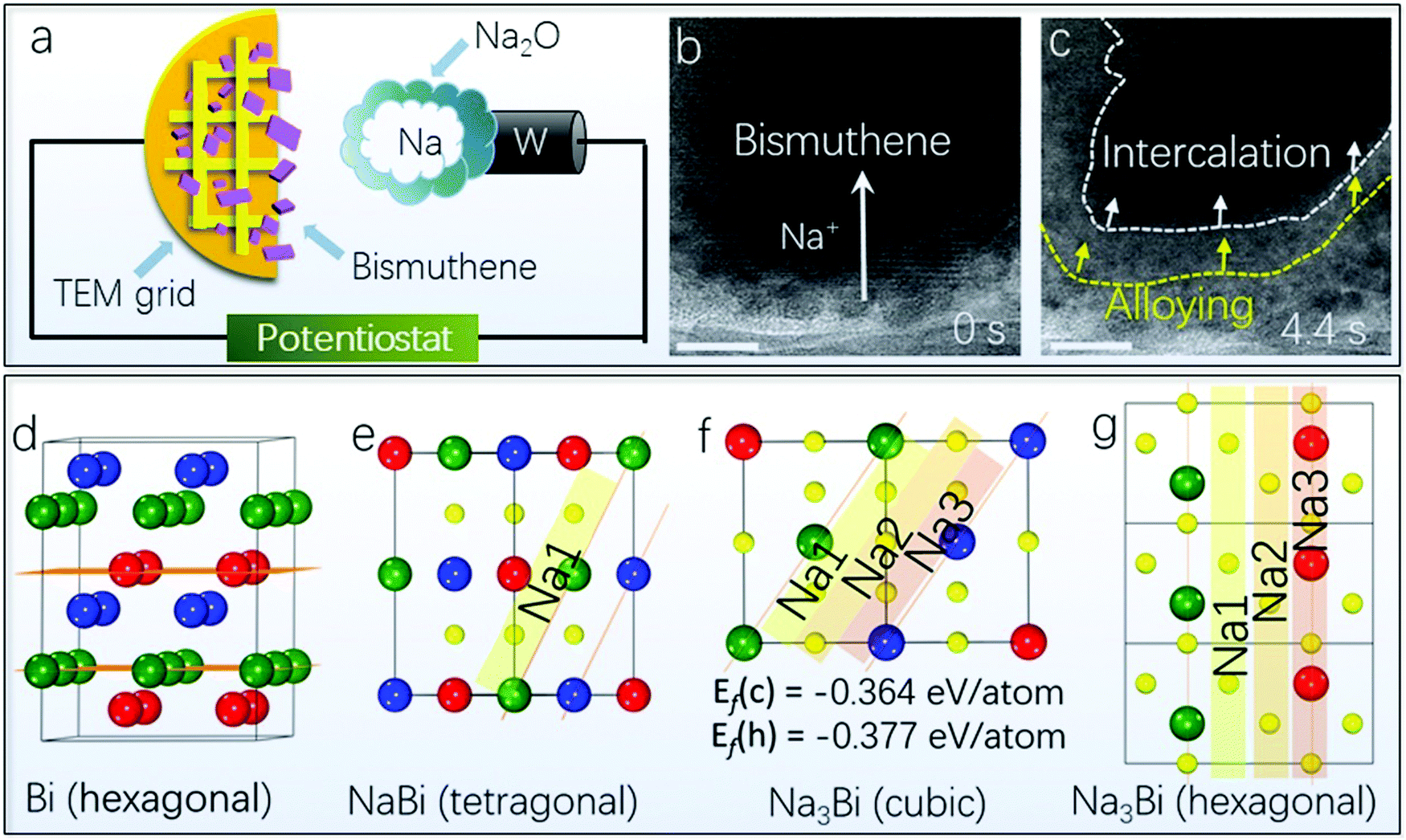 | ||
| Fig. 10 (a) Schematic depiction of the experimental setup for in situ sodiation/desodiation of 2D Bi. (b) and (c) Time-resolved HRTEM images of 2D Bi during sodiation. Scale bar: 10 nm. (d–g) Atomic structure models for different stages of phase evolutions and their plane distances. The red, green and blue spheres represent Bi atoms in different layers, whereas the yellow spheres represent Na ions (reproduced from ref. 63 with permission from the American Chemical Society, copyright 2019).63 | ||
In a parallel research, via a combination of in situ TEM and XRD characterization, Zhou et al. discovered that a large anisotropic volume expansion of 142% occurs along the z-axis due to the alloy reaction during the sodiation process. In contrast, ultrathin 2D Bi with a large aspect ratio can relieve this expansion strain.75Fig. 11a demonstrates that 2D Bi can deliver long-term cyclability with a reversible capacity of 317 mA h g−1 after 1000 cycles at a current density of 1.2 mA cm−2, indicating the good stability of 2D Bi during the charge–discharge process. Fig. 11b shows the excellent rate performance indicated by the stable capacity of 381 mA h g−1 at a current density of 0.2 mA cm−2, and it can still maintain a high reversible capacity of 263.2 mA h g−1 at a high current density of 2 mA cm−2, which is significantly higher than the low specific capacity (3.4 mA h g−1) of pure graphene at such a high current density. Remarkably, a stable and high areal sodium storage capacity as high as 12.1 mA h cm−2 can be achieved from a Bi/graphene composite electrode with tunable thickness. Moreover, the similar potential profiles of the electrodes suggest that the increased areal loading could not lead to ion diffusion obstacles owing to the highly interconnected network structure, as illustrated in Fig. 11c.75
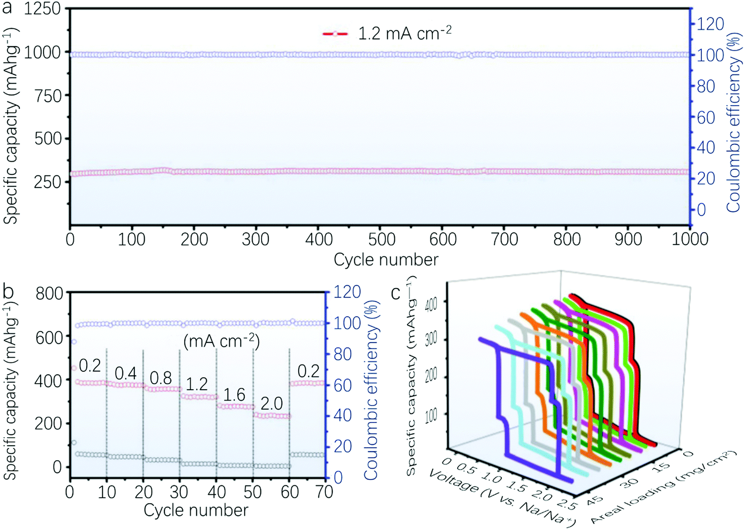 | ||
| Fig. 11 (a) Cycling performance of 2D Bi/graphene at a current density of 1.2 mA cm−2 after electrochemical pretreatment of 20 cycles at 0.05 mA cm−2. (b) Rate performance of 2D Bi/graphene and graphene films at various current densities. (c) 5th cycle potential profiles of the 2D Bi/graphene electrode samples in a range from 0.1 to 2.1 V versus Na/Na+ (reproduced from ref. 75 with permission from Wiley, copyright 2019).75 | ||
4.3. Energy conversion: CO2 reduction and N2 fixation
Electrocatalytic CO2 reduction to formate as well as N2 fixation to ammonia (NH3) have drawn increased research attention in an attempt to store renewable energy and reduce greenhouse gas emission.215–218 To be specific, CO2 can be transformed into chemical fuels by the CO2 reduction reaction (CO2RR), thereby converting electrical and solar energy in chemical bonds. Likewise, N2 can be used to produce NH3 under ambient conditions via the N2 reduction reaction (NRR). In the following, we will focus on the recent rapid development of energy-efficient environmentally friendly CO2RR and NRR processes based on 2D Bi. Besides, it should be noted that the catalytic activity of 2D Bi has also been recently investigated for the hydrogen evolution reaction (HER), oxygen evolution reaction (OER) and oxygen reduction reaction (ORR), which are important for the development of water splitting applications.20The Yanguang Li group recently conducted the CO2RR based on 2D Bi from conversion of BiOI nanosheets via a combination of theoretical and experimental studies.61Fig. 12a provides the schematic illustration of the optimized geometric structures of different states in the catalytic pathway, with the corresponding energy profiles summarized in Fig. 12b. The CO2 reduction starts with a proton-coupled electron transfer, which results in the protonation of a C or O atom. It was found that the protonation of the C atom to the OCHO* intermediate is mildly endothermic. This intermediate can be transformed into HCOO− upon the second proton-coupled electron transfer. Finally, it is released from the catalyst surface as the formate. As shown in Fig. 12b, the protonation of the O atom in CO2 to COOH* is significantly high in energy, i.e., +1.16 eV, and the free energy of H adsorption on 2D Bi is likely to be adequately positive to prohibit active HER.61 This is in accordance with the experimental results. The authors investigated the CO2RR performance of 2D Bi within a gas-tight two-compartment electrochemical cell. It was found that formate was the dominant reduction product, which is accompanied by the generation of a small amount of CO and H2. The corresponding faradaic efficiencies of different products in Fig. 12c show that the initial faradaic efficiency of formate is 16%, which increases and remains at 100% at −1.7 V. In comparison, the faradaic efficiencies of the two gaseous products remain very small at a wide spectrum of overpotentials.61 Besides, the faradaic efficiency of formate on commercial Bi nanopowder is also presented in Fig. 12c for reference. Another experimental study of the CO2RR based on 2D Bi from conversion of Bi2O2CO3 also demonstrates impressive CO2RR activity for selective CO2 reduction to formate with a large cathodic current density (∼18 mA cm−2 at −1.1 V) and a high faradaic efficiency of nearly 100% over a broad potential window.80 Furthermore, the BiOBr-templated 2D Bi catalyst can allow the CO2RR to achieve a high selectivity toward formate of over 90% and a current density as high as 200 mA cm−2, which is more than a twofold increase compared to the Bi catalysts as a comparison.169 In addition, Wang et al. have recently demonstrated a thickness-dependent activity of 2D Bi for CO2 reduction, in which the bilayer Bi exhibits the best catalytic performance among all studied 2D Bi due to the considerable stabilization energy contributed by the SOC effect.218
 | ||
| Fig. 12 CO2 and N2 reduction reactions. (a) Optimized geometric structure of CO2, OCHO* adsorbate and HCOO− in sequence used in the DFT simulations of CO2 reduction reaction processes on 2D Bi. The purple, gray, red and green spheres represent Bi, C, O and H atoms, respectively.61 (b) Free-energy diagrams of HCOO−, CO and H2 formation on 2D Bi. (c) Potential-dependent faradaic efficiencies of HCOO−, CO and H2 on 2D Bi in comparison with the faradaic efficiency of HCOO− on commercial Bi nanopowder (reproduced from ref. 61 with permission from Nature Publishing Group, copyright 2018).61 (d) NH3 formation rate and faradaic efficiency of cycles at −0.8 V versus reversible hydrogen electrode. Below: comparison of NH3 yield and faradaic efficiency of 2D Bi and Bi nanoparticles (reproduced from ref. 62 with permission from the American Chemical Society, copyright 2019).62 | ||
Regarding the N2 fixation to NH3, a mosaic 2D Bi has been recently fabricated through an in situ electrochemical reduction process, and exhibited an average NH3 yield of 2.54 ± 0.16 μg cm−2 h−1 and a faradaic efficiency of 10.46 ± 1.45% at −0.8 V versus reversible hydrogen electrode.62 The schematic illustration of the NRR activity and N2 absorption mode on mosaic 2D Bi has been previously provided in Fig. 1c, and the Bi atoms with delocalized p-electrons near the edge sites could offer abundant catalytic active sites for the adsorption and activation of N2. The stability of the 2D Bi electrocatalyst is investigated by cycling and chronoamperometric measurements at −0.8 V versus reversible hydrogen electrode. It was found that there was no significant current density loss during the electrolysis process for 25 hours. Besides, after six cycling tests, the NH3 yield and the faradaic efficiency did not decrease obviously, as shown in the upper part of Fig. 12d.62 In addition, the NRR performance of mosaic 2D Bi and Bi nanoparticles is compared in the lower panel of Fig. 12d, demonstrating that the NH3 yield and the faradaic efficiency of Bi nanoparticles are significantly inferior to those of mosaic 2D Bi under the same experimental conditions. However, it bears mentioning that the faradaic efficiency can also be remarkably increased by a strategy using a combination of 2D nanoparticles and potassium cations, in which the potassium cations can stabilize key N2-reduction intermediates and regulate proton transfer to increase the selectivity.219 In addition, 2D Bi array on a Cu foil can be treated as a stable 3D catalyst electrode with a high faradaic efficiency of 10.26%.220
5. Conclusions and outlook
Derived from the last element of the group VA column, 2D Bi has exhibited superior properties for energy-related applications, such as the largest SOC-induced bulk gap, large charge carrier mobility, highest theoretical volume capacity among group VA materials, and high intrinsic CO2RR and NRR activity. Its excellent structure stability, thermodynamic stability, experimentally confirmed air stability as well as non-toxicity and environmental friendliness bring more optimism in developing reliable low-cost state-of-the-art devices for energy applications.Various fabrication techniques have been gradually improved in the past several years to obtain high-quality 2D Bi, mainly including liquid exfoliation, hot-pressing, PVD, PLD and wet chemical methods. These fabrication methods of 2D Bi so far excel in different aspects of energy-related applications. For instance, the accurate control of the 2D Bi ultrathin thickness used for TI investigations requires ultrahigh vacuum conditions, resulting in the requirement of an expensive MBE system coupled with advanced in situ characterization apparatus that further brings high experimental cost and low fabrication efficiency. In comparison, 2D Bi used for battery and energy conversion applications is usually obtained via low-cost and efficient liquid exfoliation as well as wet chemical methods, which are indeed more straightforward to apply, but problems still exist such as how to further improve the yield and how to completely remove solvent from the final products. These pros and cons of different fabrication methods to obtain 2D Bi somehow resemble the initial development of organic semiconductors more than two decades ago, for which MBE and solution processes have been mainly targeted for small-molecule and polymer organic semiconductors, respectively.221 Combining the high-quality and low-cost characteristics, the future fabrication methods of 2D Bi could be further significantly improved and optimized even for mass production, assisted by the development experience from other material systems.
The unique superior properties of 2D Bi make it suitable for the fabrication of state-of-the-art devices in energy sciences, such as energy-dissipationless topological insulators for energy-saving purposes, newly-designed batteries for energy storage as well as electrochemistry-involved devices aiming at CO2 reduction and N2 fixation. In terms of TI investigation, fully-planar 2D Bi on a SiC(0001) substrate has exhibited the largest experimentally determined bulk gap of 800 meV so far, which renders 2D Bi the most promising candidate for constructing cryogenic-free TI-based devices. Moreover, if 2D Bi is further coupled with graphene, beneficial for long distance spin transport, more reliable spin-to-charge conversion could be realized for next-generation spintronic devices.222 A programmed vacuum stack process could be applied to realize this vertical composition of 2D Bi and other 2D building blocks with atomic-scale precision even on an entire wafer.223 A major bottleneck to the investigation of 2D Bi TI is the requirement of complicated characterization techniques combining ARPES, STM and STS, and more intensive research efforts should be devoted to further figuring out systematic and comprehensive fabrication and characterization procedures, assisted by which the research focus in future can be shifted to direct transport measurements directly on 2D Bi-based devices.224 As for energy storage, especially for sodium-ion batteries, the intercalation and alloying processes of few-layer 2D Bi for sodium storage have been recently revealed using in situ characterization methods. Moreover, the improved areal capacity of a newly-designed 2D Bi-integrated unit can open up new opportunities to develop high-performance batteries. Regarding energy conversion, the experimental achievements in terms of CO2 reduction and N2 fixation based on 2D Bi stand out in front of the other electrochemistry-involved applications. The corresponding large cathodic current density and high faradaic efficiency based on 2D Bi in the CO2RR and NRR clearly demonstrate great opportunities for more advanced energy conversion systems. Apart from the aforementioned scenarios in energy saving-, storage- and conversion-devices, the excellent investigations based on 2D Bi have also planted the seeds of tremendous innovation around other intriguing applications, such as thermoelectricity, optoelectronics and photonics,84,173 representing another step toward a brighter future to explore 2D Bi for more reliable potential applications.
Furthermore, the recent research forefront, i.e., unconventional electronic and optical properties, originated from the moiré superlattice of 2D materials,206,225–229 could inspire further intriguing studies on 2D Bi in energy sciences. The improved fabrication and manipulation techniques of bismuthene, along with its unique properties, might enable 2D Bi to play an important role in the newly-developed research field of twistronics.230–232 It can be optimistically speculated that the future research outcomes of 2D Bi in energy sciences could make its existing encouraging studies appear to be low-hanging fruits. We hope that this review article will inspire further investigations regarding 2D Bi for more valuable energy-related applications.
Conflicts of interest
There are no conflicts to declare.Acknowledgements
The authors acknowledge financial support from the Fundamental Research Funds for the Central Universities (No. 30919011109), the Natural Science Foundation of Jiangsu Province (BK20180071), the Qing Lan Project of Jiangsu Province, the Six Talent Peaks Project of Jiangsu Province (Grant No. XCL-035), and Martin Pumera acknowledges the financial support of Grant Agency of the Czech Republic (EXPRO: 19-26896X). We also thank Dr Yaxin Huang for valuable discussions.References
- A. J. Mannix, B. Kiraly, M. C. Hersam and N. P. Guisinger, Nat. Rev. Chem., 2017, 1, 0014 CrossRef CAS.
- K. S. Novoselov, A. Mishchenko, A. Carvalho and A. H. Castro Neto, Science, 2016, 353, 9439 CrossRef.
- K. S. Novoselov, A. K. Geim, S. V. Morozov, D. Jiang, Y. Zhang, S. V. Dubonos, I. V. Grigorieva and A. A. Firsov, Science, 2004, 306, 666–669 CrossRef CAS.
- R. Mas-Balleste, C. Gomez-Navarro, J. Gomez-Herrero and F. Zamora, Nanoscale, 2011, 3, 20–30 RSC.
- J. Liu and X.-W. Liu, Adv. Mater., 2012, 24, 4097–4111 CrossRef CAS PubMed.
- M. Zhou, X. W. Lou and Y. Xie, Nano Today, 2013, 8, 598–618 CrossRef CAS.
- G. Fiori, F. Bonaccorso, G. Iannaccone, T. Palacios, D. Neumaier, A. Seabaugh, S. K. Banerjee and L. Colombo, Nat. Nanotechnol., 2014, 9, 768–779 CrossRef CAS PubMed.
- G. R. Bhimanapati, Z. Lin, V. Meunier, Y. Jung, J. Cha, S. Das, D. Xiao, Y. Son, M. S. Strano, V. R. Cooper, L. Liang, S. G. Louie, E. Ringe, W. Zhou, S. S. Kim, R. R. Naik, B. G. Sumpter, H. Terrones, F. Xia, Y. Wang, J. Zhu, D. Akinwande, N. Alem, J. A. Schuller, R. E. Schaak, M. Terrones and J. A. Robinson, ACS Nano, 2015, 9, 11509–11539 CrossRef CAS PubMed.
- C. Tan, Z. Liu, W. Huang and H. Zhang, Chem. Soc. Rev., 2015, 44, 2615–2628 RSC.
- Z. Lin, A. McCreary, N. Briggs, S. Subramanian, K. Zhang, Y. Sun, X. Li, N. J. Borys, H. Yuan, S. K. Fullerton-Shirey, A. Chernikov, H. Zhao, S. McDonnell, A. M. Lindenberg, K. Xiao, B. J. LeRoy, M. Drndic, J. C. M. Hwang, J. Park, M. Chhowalla, R. E. Schaak, A. Javey, M. C. Hersam, J. Robinson and M. Terrones, 2D Mater., 2016, 3, 042001 CrossRef.
- C. Tan, X. Cao, X.-J. Wu, Q. He, J. Yang, X. Zhang, J. Chen, W. Zhao, S. Han, G.-H. Nam, M. Sindoro and H. Zhang, Chem. Rev., 2017, 117, 6225–6331 CrossRef CAS PubMed.
- Z. Cai, B. Liu, X. Zou and H.-M. Cheng, Chem. Rev., 2018, 118, 6091–6133 CrossRef CAS PubMed.
- H. Jin, C. Guo, X. Liu, J. Liu, A. Vasileff, Y. Jiao, Y. Zheng and S.-Z. Qiao, Chem. Rev., 2018, 118, 6337–6408 CrossRef CAS PubMed.
- Z. Wang, J. Qiu, X. Wang, Z. Zhang, Y. Chen, X. Huang and W. Huang, Chem. Soc. Rev., 2018, 47, 6128–6174 RSC.
- F. Yi, H. Ren, J. Shan, X. Sun, D. Wei and Z. Liu, Chem. Soc. Rev., 2018, 47, 3152–3188 RSC.
- P. Zhang, F. Wang, M. Yu, X. Zhuang and X. Feng, Chem. Soc. Rev., 2018, 47, 7426–7451 RSC.
- N. Mounet, M. Gibertini, P. Schwaller, D. Campi, A. Merkys, A. Marrazzo, T. Sohier, I. E. Castelli, A. Cepellotti, G. Pizzi and N. Marzari, Nat. Nanotechnol., 2018, 13, 246–252 CrossRef CAS PubMed.
- Y. Liu, F. Xu, Z. Zhang, E. S. Penev and B. I. Yakobson, Nano Lett., 2014, 14, 6782–6786 CrossRef CAS PubMed.
- P. Perumal, R. K. Ulaganathan, R. Sankar, Y.-M. Liao, T.-M. Sun, M.-W. Chu, F. C. Chou, Y.-T. Chen, M.-H. Shih and Y.-F. Chen, Adv. Funct. Mater., 2016, 26, 3630–3638 CrossRef CAS.
- R. Gusmao, Z. Sofer, D. Bousa and M. Pumera, Angew. Chem., Int. Ed., 2017, 56, 14417–14422 CrossRef CAS.
- T. Low, A. Chaves, J. D. Caldwell, A. Kumar, N. X. Fang, P. Avouris, T. F. Heinz, F. Guinea, L. Martin-Moreno and F. Koppens, Nat. Mater., 2017, 16, 182–194 CrossRef CAS.
- L. Britnell, R. M. Ribeiro, A. Eckmann, R. Jalil, B. D. Belle, A. Mishchenko, Y. J. Kim, R. V. Gorbachev, T. Georgiou, S. V. Morozov, A. N. Grigorenko, A. K. Geim, C. Casiraghi, A. H. Castro Neto and K. S. Novoselov, Science, 2013, 340, 1311–1314 CrossRef CAS PubMed.
- H. Li, Y. Li, A. Aljarb, Y. Shi and L.-J. Li, Chem. Rev., 2018, 118, 6134–6150 CrossRef CAS PubMed.
- X. Duan, C. Wang, A. Pan, R. Yu and X. Duan, Chem. Soc. Rev., 2015, 44, 8859–8876 RSC.
- J. Sun, C. Lu, Y. Song, Q. Ji, X. Song, Q. Li, Y. Zhang, L. Zhang, J. Kong and Z. Liu, Chem. Soc. Rev., 2018, 47, 4242–4257 RSC.
- Z. Y. Al Balushi, K. Wang, R. K. Ghosh, R. A. Vila, S. M. Eichfeld, J. D. Caldwell, X. Y. Qin, Y. C. Lin, P. A. DeSario, G. Stone, S. Subramanian, D. F. Paul, R. M. Wallace, S. Datta, J. M. Redwing and J. A. Robinson, Nat. Mater., 2016, 15, 1166–1171 CrossRef CAS PubMed.
- S. T. Ha, X. F. Liu, Q. Zhang, D. Giovanni, T. C. Sum and Q. H. Xiong, Adv. Opt. Mater., 2014, 2, 838–844 CrossRef CAS.
- X. Liu, D. Yu, C. Huo, X. Song, Y. Gao, S. Zhang and H. Zeng, Adv. Opt. Mater., 2018, 6, 1800206 CrossRef.
- X. Liu, D. Yu, X. Song and H. Zeng, Small, 2018, 14, 1801460 CrossRef PubMed.
- E. Shi, Y. Gao, B. P. Finkenauer, Akriti, A. H. Coffey and L. Dou, Chem. Soc. Rev., 2018, 47, 6046–6072 RSC.
- K. S. Novoselov, Rev. Mod. Phys., 2011, 83, 837–849 CrossRef CAS.
- K. S. Novoselov, V. I. Fal'ko, L. Colombo, P. R. Gellert, M. G. Schwab and K. Kim, Nature, 2012, 490, 192–200 CrossRef CAS PubMed.
- Y. Liu, X. Duan, Y. Huang and X. Duan, Chem. Soc. Rev., 2018, 47, 6388–6409 RSC.
- W. Han, K. Pi, K. M. McCreary, Y. Li, J. J. I. Wong, A. G. Swartz and R. K. Kawakami, Phys. Rev. Lett., 2010, 105, 167202 CrossRef PubMed.
- W. Han, R. K. Kawakami, M. Gmitra and J. Fabian, Nat. Nanotechnol., 2014, 9, 794–807 CrossRef CAS PubMed.
- L. Tao, E. Cinquanta, D. Chiappe, C. Grazianetti, M. Fanciulli, M. Dubey, A. Molle and D. Akinwande, Nat. Nanotechnol., 2015, 10, 227–231 CrossRef CAS PubMed.
- A. Acun, L. Zhang, P. Bampoulis, M. Farmanbar, A. van Houselt, A. N. Rudenko, M. Lingenfelder, G. Brocks, B. Poelsema, M. I. Katsnelson and H. J. W. Zandvliet, J. Phys.: Condens. Matter, 2015, 27, 443002 CrossRef CAS PubMed.
- F.-f. Zhu, W.-j. Chen, Y. Xu, C.-l. Gao, D.-d. Guan, C.-h. Liu, D. Qian, S.-C. Zhang and J.-f. Jia, Nat. Mater., 2015, 14, 1020–1025 CrossRef CAS PubMed.
- S. J. Zaveh, M. R. Roknabadi, T. Morshedloo and M. Modarresi, Superlattices Microstruct., 2016, 91, 383–390 CrossRef.
- R. John and B. Merlin, J. Phys. Chem. Solids, 2017, 110, 307–315 CrossRef CAS.
- B. Mortazavi, O. Rahaman, M. Makaremi, A. Dianat, G. Cuniberti and T. Rabczuk, Physica E, 2017, 87, 228–232 CrossRef CAS.
- A. Molle, C. Grazianetti, L. Tao, D. Taneja, M. H. Alam and D. Akinwande, Chem. Soc. Rev., 2018, 47, 6370–6387 RSC.
- A. Bansil, H. Lin and T. Das, Rev. Mod. Phys., 2016, 88, 021004 CrossRef.
- L. Li, Y. Yu, G. J. Ye, Q. Ge, X. Ou, H. Wu, D. Feng, X. H. Chen and Y. Zhang, Nat. Nanotechnol., 2014, 9, 372–377 CrossRef CAS PubMed.
- F. Ersan, E. Akturk and S. Ciraci, Phys. Rev. B, 2016, 94, 245417 CrossRef.
- S.-S. Li, W.-X. Ji, P. Li, S.-J. Hu, T. Zhou, C.-W. Zhang and S.-S. Yan, Sci. Rep., 2017, 7, 6126 CrossRef PubMed.
- F. Dominguez, B. Scharf, G. Li, J. Schaefer, R. Claessen, W. Hanke, R. Thomale and E. M. Hankiewicz, Phys. Rev. B, 2018, 98, 161407 CrossRef CAS.
- S. Cui, H. Pu, S. A. Wells, Z. Wen, S. Mao, J. Chang, M. C. Hersam and J. Chen, Nat. Commun., 2015, 6, 8632 CrossRef CAS PubMed.
- J. Ji, X. Song, J. Liu, Z. Yan, C. Huo, S. Zhang, M. Su, L. Liao, W. Wang, Z. Ni, Y. Hao and H. Zeng, Nat. Commun., 2016, 7, 13352 CrossRef CAS PubMed.
- P. Chen, N. Li, X. Chen, W.-J. Ong and X. Zhao, 2D Mater., 2018, 5, 014002 CrossRef.
- K. Zhang, B. Jin, C. Park, Y. Cho, X. Song, X. Shi, S. Zhang, W. Kim, H. Zeng and J. H. Park, Nat. Commun., 2019, 10, 2001 CrossRef.
- L. Li, L. Chen, S. Mukherjee, J. Gao, H. Sun, Z. Liu, X. Ma, T. Gupta, C. V. Singh, W. Ren, H.-M. Cheng and N. Koratkar, Adv. Mater., 2017, 29, 1602734 CrossRef PubMed.
- W. Tian, S. Zhang, C. Huo, D. Zhu, Q. Li, L. Wang, X. Ren, L. Xie, S. Guo, P. K. Chu, H. Zeng and K. Huo, ACS Nano, 2018, 12, 1887–1893 CrossRef CAS PubMed.
- S. M. Beladi-Mousavi and M. Pumera, Chem. Soc. Rev., 2018, 47, 6964–6989 RSC.
- F. Reis, G. Li, L. Dudy, M. Bauernfeind, S. Glass, W. Hanke, R. Thomale, J. Schafer and R. Claessen, Science, 2017, 357, 287–290 CrossRef CAS PubMed.
- S. Zhang, M. Xie, F. Li, Z. Yan, Y. Li, E. Kan, W. Liu, Z. Chen and H. Zeng, Angew. Chem., Int. Ed., 2016, 55, 1666–1669 CrossRef CAS.
- E. Saitoh, M. Ueda, H. Miyajima and G. Tatara, Appl. Phys. Lett., 2006, 88, 182509 CrossRef.
- J. C. Rojas Sanchez, L. Vila, G. Desfonds, S. Gambarelli, J. P. Attane, J. M. De Teresa, C. Magen and A. Fert, Nat. Commun., 2013, 4, 2944 CrossRef PubMed.
- S. Manipatruni, D. E. Nikonov and I. A. Young, Nat. Phys., 2018, 14, 338–343 Search PubMed.
- E. S. Walker, S. R. Na, D. Jung, S. D. March, J.-S. Kim, T. Trivedi, W. Li, L. Tao, M. L. Lee, K. M. Liechti, D. Akinwande and S. R. Bank, Nano Lett., 2016, 16, 6931–6938 CrossRef CAS PubMed.
- N. Han, Y. Wang, H. Yang, J. Deng, J. Wu, Y. Li and Y. Li, Nat. Commun., 2018, 9, 1320 CrossRef PubMed.
- L. Li, C. Tang, B. Xia, H. Jin, Y. Zheng and S.-Z. Qiao, ACS Catal., 2019, 9, 2902–2908 CrossRef CAS.
- Y. Huang, C. Zhu, S. Zhang, X. Hu, K. Zhang, W. Zhou, S. Guo, F. Xu and H. Zeng, Nano Lett., 2019, 19, 1118–1123 CrossRef PubMed.
- Y. M. Koroteev, G. Bihlmayer, J. E. Gayone, E. V. Chulkov, S. Blugel, P. M. Echenique and P. Hofmann, Phys. Rev. Lett., 2004, 93, 046403 CrossRef PubMed.
- T. Hirahara, T. Nagao, I. Matsuda, G. Bihlmayer, E. V. Chulkov, Y. M. Koroteev, P. M. Echenique, M. Saito and S. Hasegawa, Phys. Rev. Lett., 2006, 97, 146803 CrossRef CAS PubMed.
- L. Kou, X. Tan, Y. Ma, H. Tahini, L. Zhou, Z. Sun, A. Du, C. Chen and S. C. Smith, 2D Mater., 2015, 2, 045010 CrossRef.
- X. Wang, C. Xu, H. Hu, P. Wang, G. Bian, W. Tan, S. A. Brown and T. C. Chiang, EPL, 2017, 119, 27002 CrossRef.
- S.-C. Chen, J.-Y. Wu and M.-F. Lin, New J. Phys., 2018, 20, 062001 CrossRef.
- J. Kim and R. Wu, Phys. Rev. B, 2018, 97, 115151 CrossRef CAS.
- L. Kou, H. Fu, Y. Ma, B. Yan, T. Liao, A. Du and C. Chen, Phys. Rev. B, 2018, 97, 075429 CrossRef.
- Y. Guo, F. Pan, M. Ye, X. Sun, Y. Wang, J. Li, X. Zhang, H. Zhang, Y. Pan, Z. Song, J. Yang and J. Lu, ACS Appl. Mater. Interfaces, 2017, 9, 23128–23140 CrossRef CAS PubMed.
- P. Zhao, W. Wei, Q. Sun, L. Yu, B. Huang and Y. Dai, Nanotechnology, 2017, 28, 255201 CrossRef PubMed.
- J. D. Yao, J. M. Shao and G. W. Yang, Sci. Rep., 2015, 5, 12320 CrossRef CAS PubMed.
- H. Hao, R. Xiaohui, L. Zhongjun, W. Huide, H. Zongyu, Q. Hui, T. Pinghua, Z. Jinlai, L. Weiyuan, G. Yanqi, L. Jie, L. Jianqing, Q. Xiang and Z. Han, Nanotechnology, 2018, 29, 235201 CrossRef PubMed.
- J. Zhou, J. Chen, M. Chen, J. Wang, X. Liu, B. Wei, Z. Wang, J. Li, L. Gu, Q. Zhang, H. Wang and L. Guo, Adv. Mater., 2019, 31, 1807874 CrossRef PubMed.
- S. Kim, W. J. Dong, S. Gim, W. Sohn, J. Y. Park, C. J. Yoo, H. W. Jang and J.-L. Lee, Nano Energy, 2017, 39, 44–52 CrossRef CAS.
- S. He, F. Ni, Y. Ji, L. Wang, Y. Wen, H. Bai, G. Liu, Y. Zhang, Y. Li, B. Zhang and H. Peng, Angew. Chem., Int. Ed., 2018, 57, 16114–16119 CrossRef CAS.
- W. Oh, C. K. Rhee, J. W. Han and B. Shong, J. Phys. Chem. C, 2018, 122, 23084–23090 CrossRef CAS.
- P. Su, W. Xu, Y. Qiu, T. Zhang, X. Li and H. Zhang, ChemSusChem, 2018, 11, 848–853 CrossRef CAS PubMed.
- H. Yang, N. Han, J. Deng, J. Wu, Y. Wang, Y. Hu, P. Ding, Y. Li, Y. Li and J. Lu, Adv. Energy Mater., 2018, 8, 1801536 CrossRef.
- W. Zhang, Y. Hu, L. Ma, G. Zhu, P. Zhao, X. Xue, R. Chen, S. Yang, J. Ma, J. Liu and Z. Jin, Nano Energy, 2018, 53, 808–816 CrossRef CAS.
- Y. Zhang, X. Zhang, Y. Ling, F. Li, A. M. Bond and J. Zhang, Angew. Chem., Int. Ed., 2018, 57, 13283–13287 CrossRef CAS PubMed.
- J. Zhang, S.-X. Guo, Y. Zhang, X. Zhang, C. D. Easton and D. R. MacFarlane, ChemSusChem, 2019, 1802409 Search PubMed.
- L. Lu, Z. Liang, L. Wu, Y. Chen, Y. Song, S. C. Dhanabalan, J. S. Ponraj, B. Dong, Y. Xiang, F. Xing, D. Fan and H. Zhang, Laser Photonics Rev., 2018, 12, 1700221 CrossRef.
- H. L. Chia, N. M. Latiff, R. Gusmao, Z. Sofer and M. Pumera, Chem. – Eur. J., 2019, 25, 2242–2249 CrossRef CAS PubMed.
- M. Jankowski, D. Kaminski, K. Vergeer, M. Mirolo, F. Carla, G. Rijnders and T. R. J. Bollmann, Nanotechnology, 2017, 28, 155602 CrossRef.
- S. Zhang, S. Guo, Z. Chen, Y. Wang, H. Gao, J. Gomez-Herrero, P. Ares, F. Zamora, Z. Zhu and H. Zeng, Chem. Soc. Rev., 2018, 47, 982–1021 RSC.
- M. Pumera and Z. Sofer, Adv. Mater., 2017, 29, 1605299 CrossRef PubMed.
- H. Iwasaki and T. Kikegawa, Acta Crystallogr., Sect. B: Struct. Sci., 1997, 53, 353–357 CrossRef.
- T. Nagao, J. T. Sadowski, M. Saito, S. Yaginuma, Y. Fujikawa, T. Kogure, T. Ohno, Y. Hasegawa, S. Hasegawa and T. Sakurai, Phys. Rev. Lett., 2004, 93, 105501 CrossRef CAS.
- P. J. Kowalczyk, O. Mahapatra, M. Le Ster, S. A. Brown, G. Bian, X. Wang and T. C. Chiang, Phys. Rev. B, 2017, 96, 205434 CrossRef.
- Y. Lu, W. Xu, M. Zeng, G. Yao, L. Shen, M. Yang, Z. Luo, F. Pan, K. Wu, T. Das, P. He, J. Jiang, J. Martin, Y. P. Feng, H. Lin and X.-S. Wang, Nano Lett., 2015, 15, 80–87 CrossRef CAS PubMed.
- K. Yamada, S. Souma, K. Yamauchi, N. Shimamura, K. Sugawara, C. X. Trang, T. Oguchi, K. Ueno, T. Takahashi and T. Sato, Nano Lett., 2018, 18, 3235–3240 CrossRef CAS PubMed.
- H.-H. Sun, M.-X. Wang, F. Zhu, G.-Y. Wang, H.-Y. Ma, Z.-A. Xu, Q. Liao, Y. Lu, C.-L. Gao, Y.-Y. Li, C. Liu, D. Qian, D. Guan and J.-F. Jia, Nano Lett., 2017, 17, 3035–3039 CrossRef CAS PubMed.
- C.-H. Hsu, Z.-Q. Huang, F.-C. Chuang, C.-C. Kuo, Y.-T. Liu, H. Lin and A. Bansil, New J. Phys., 2015, 17, 025005 CrossRef.
- T. D. Huan, M. Amsler, R. Sabatini, V. N. Tuoc, N. B. Le, L. M. Woods, N. Marzari and S. Goedecker, Phys. Rev. B: Condens. Matter Mater. Phys., 2013, 88, 024108 CrossRef.
- B. T. Wang, P. Zhang, R. Lizarraga, I. Di Marco and O. Eriksson, Phys. Rev. B: Condens. Matter Mater. Phys., 2013, 88, 104107 CrossRef.
- J. Dai and X. C. Zeng, Angew. Chem., Int. Ed., 2015, 54, 7572–7576 CrossRef CAS PubMed.
- E. Akturk, O. U. Akturk and S. Ciraci, Phys. Rev. B, 2016, 94, 014115 CrossRef.
- H. Liu, Y. C. Du, Y. X. Deng and P. D. Ye, Chem. Soc. Rev., 2015, 44, 2732–2743 RSC.
- C. Hao, F. Wen, J. Xiang, S. Yuan, B. Yang, L. Li, W. Wang, Z. Zeng, L. Wang, Z. Liu and Y. Tian, Adv. Funct. Mater., 2016, 26, 2016–2024 CrossRef CAS.
- J. Pei, X. Gai, J. Yang, X. Wang, Z. Yu, D.-Y. Choi, B. Luther-Davies and Y. Lu, Nat. Commun., 2016, 7, 10450 CrossRef CAS PubMed.
- M. Serrano-Ruiz, M. Caporali, A. Ienco, V. Piazza, S. Heun and M. Peruzzini, Adv. Mater. Interfaces, 2016, 3, 1500441 CrossRef PubMed.
- G. Wang, W. J. Slough, R. Pandey and S. P. Karna, 2D Mater., 2016, 3, 025011 CrossRef.
- A. A. Kistanov, S. K. Khadiullin, K. Zhou, S. V. Dmitriev and E. A. Korznikova, J. Mater. Chem. C, 2019, 7, 9195–9202 RSC.
- A. Ziletti, A. Carvalho, D. K. Campbell, D. F. Coker and A. H. C. Neto, Phys. Rev. Lett., 2015, 114, 046801 CrossRef CAS PubMed.
- D. Cahen and A. Kahn, Adv. Mater., 2003, 15, 271–277 CrossRef CAS.
- P. I. Djurovich, E. I. Mayo, S. R. Forrest and M. E. Thompson, Org. Electron., 2009, 10, 515–520 CrossRef CAS.
- K. Premasiri and X. P. A. Gao, J. Phys.: Condens. Matter, 2019, 31, 193001 CrossRef CAS PubMed.
- I. Gierz, T. Suzuki, E. Frantzeskakis, S. Pons, S. Ostanin, A. Ernst, J. Henk, M. Grioni, K. Kern and C. R. Ast, Phys. Rev. Lett., 2009, 103, 046803 CrossRef CAS PubMed.
- D. V. Khomitsky, Phys. Rev. B: Condens. Matter Mater. Phys., 2009, 79, 205401 CrossRef.
- J. Zhao, W. L. Guo and J. Ma, Nano Res., 2017, 10, 491 CrossRef CAS.
- Y. M. Koroteev, G. Bihlmayer, E. V. Chulkov and S. Blügel, Phys. Rev. B: Condens. Matter Mater. Phys., 2008, 77, 045428 CrossRef.
- R. R. Q. Freitas, R. Rivelino, F. de Brito Mota, C. M. C. de Castilho, A. Kakanakova-Georgieva and G. K. Gueorguiev, J. Phys. Chem. C, 2015, 119, 23599–23606 CrossRef CAS.
- Z. Yang, Z. Wu, Y. Lyu and J. Hao, InfoMat, 2019, 1, 98–107 CrossRef.
- S. Coe-Sullivan, W. Liu, P. Allen and J. S. Steckel, ECS J. Solid State Sci. Technol., 2013, 2, R3026–R3030 CrossRef CAS.
- Z. Liu, K. Zhao, A. Tang, Y. Xie, L. Qian, W. Cao, Y. Yang, Y. Chen and F. Teng, Org. Electron., 2016, 36, 97–102 CrossRef CAS.
- H. C. Wang, H. Zhang, H. Y. Chen, H. C. Yeh, M. R. Tseng, R. J. Chung, S. Chen and R. S. Liu, Small, 2017, 13, 1603962 CrossRef PubMed.
- D. H. Kim, S. H. Lee, J. K. Kim and G. H. Lee, Appl. Surf. Sci., 2006, 252, 3525–3531 CrossRef CAS.
- S. E. Rodil, O. Garcia-Zarco, E. Camps, H. Estrada, M. Lejeune, L. Bourja and A. Zeinert, Thin Solid Films, 2017, 636, 384–391 CrossRef CAS.
- Y. Zhou, W. Li, Q. Zhang, S. Yan, Y. Cao, F. Dong and F. Wang, Phys. Chem. Chem. Phys., 2017, 19, 25610–25616 RSC.
- I. K. Drozdov, A. Alexandradinata, S. Jeon, S. Nadj-Perge, H. Ji, R. J. Cava, B. A. Bernevig and A. Yazdani, Nat. Phys., 2014, 10, 664–669 Search PubMed.
- Z. Guo, H. Zhang, S. Lu, Z. Wang, S. Tang, J. Shao, Z. Sun, H. Xie, H. Wang, X.-F. Yu and P. K. Chu, Adv. Funct. Mater., 2015, 25, 6996–7002 CrossRef CAS.
- C. Gibaja, D. Rodriguez-San-Miguel, P. Ares, J. Gomez-Herrero, M. Varela, R. Gillen, J. Maultzsch, F. Hauke, A. Hirsch, G. Abellan and F. Zamora, Angew. Chem., Int. Ed., 2016, 55, 14343–14347 Search PubMed.
- S. M. Beladi-Mousavi, A. M. Pourrahimi, Z. Sofer and M. Pumera, Adv. Funct. Mater., 2019, 29, 1807004 Search PubMed.
- L. Lu, W. Wang, L. Wu, X. Jiang, Y. Xiang, J. Li, D. Fan and H. Zhang, ACS Photonics, 2017, 4, 2852–2861 CrossRef CAS.
- T. Chai, X. Li, T. Feng, P. Guo, Y. Song, Y. Chen and H. Zhang, Nanoscale, 2018, 10, 17617–17622 RSC.
- B. Guo, S.-H. Wang, Z.-X. Wu, Z.-X. Wang, D.-H. Wang, H. Huang, F. Zhang, Y.-Q. Ge and H. Zhang, Opt. Express, 2018, 26, 22750–22760 CrossRef CAS PubMed.
- Y. Wang, W. Huang, J. Zhao, H. Huang, C. Wang, F. Zhang, J. Liu, J. Li, M. Zhang and H. Zhang, J. Mater. Chem. C, 2019, 7, 871–878 RSC.
- Q.-Q. Yang, R.-T. Liu, C. Huang, Y.-F. Huang, L.-F. Gao, B. Sun, Z.-P. Huang, L. Zhang, C.-X. Hu, Z.-Q. Zhang, C.-L. Sun, Q. Wang, Y.-L. Tang and H.-L. Zhang, Nanoscale, 2018, 10, 21106–21115 RSC.
- C. C. Mayorga-Martinez, R. Gusmao, Z. Sofer and M. Pumera, Angew. Chem., Int. Ed., 2019, 58, 134–138 CrossRef CAS.
- N. Hussain, T. Liang, Q. Zhang, T. Anwar, Y. Huang, J. Lang, K. Huang and H. Wu, Small, 2017, 13, 1701349 CrossRef PubMed.
- T. Nagao, S. Yaginuma, M. Saito, T. Kogure, J. T. Sadowski, T. Ohno, S. Hasegawa and T. Sakurai, Surf. Sci., 2005, 590, L247–L252 CrossRef CAS.
- T. Hirahara, G. Bihlmayer, Y. Sakamoto, M. Yamada, H. Miyazaki, S. Kimura, S. Blugel and S. Hasegawa, Phys. Rev. Lett., 2011, 107, 166801 CrossRef PubMed.
- F. Yang, L. Miao, Z. F. Wang, M. Y. Yao, F. F. Zhu, Y. R. Song, M. X. Wang, J. P. Xu, A. V. Fedorov, Z. Sun, G. B. Zhang, C. H. Liu, F. Liu, D. Qian, C. L. Gao and J. F. Jia, Phys. Rev. Lett., 2012, 109, 016801 CrossRef PubMed.
- M. Chen, J. P. Peng, H. M. Zhang, L. L. Wang, K. He, X. C. Ma and Q. K. Xue, Appl. Phys. Lett., 2012, 101, 081603 CrossRef.
- S. A. Scott, M. V. Kral and S. A. Brown, Surf. Sci., 2005, 587, 175–184 CrossRef CAS.
- D. N. McCarthy, D. Robertson, P. J. Kowalczyk and S. A. Brown, Surf. Sci., 2010, 604, 1273–1282 CrossRef CAS.
- P. J. Kowalczyk, O. Mahapatra, D. N. McCarthy, W. Kozlowski, Z. Klusek and S. A. Brown, Surf. Sci., 2011, 605, 659–667 CrossRef CAS.
- P. J. Kowalczyk, O. Mahapatra, D. Belic, S. A. Brown, G. Bian and T. C. Chiang, Phys. Rev. B: Condens. Matter Mater. Phys., 2015, 91, 045434 CrossRef.
- F. Song, J. W. Wells, Z. Jiang, M. Saxegaard and E. Wahlstrom, ACS Appl. Mater. Interfaces, 2015, 7, 8525–8532 CrossRef CAS.
- N. Kawakami, C. L. Lin, K. Kawahara, M. Kawai, R. Arafune and N. Takagi, Phys. Rev. B, 2017, 96, 205402 CrossRef.
- H. Hattab, E. Zubkov, A. Bernhart, G. Jnawali, C. Bobisch, B. Krenzer, M. Acet, R. Möller and M. Horn-vonHoegen, Thin Solid Films, 2008, 516, 8227 CrossRef CAS.
- L. M. Canonico, T. G. Rappoport and R. B. Muniz, Phys. Rev. Lett., 2019, 122, 196601 CrossRef CAS PubMed.
- A. Fang, C. Adamo, S. Jia, R. J. Cava, S.-C. Wu, C. Felser and A. Kapitulnik, Sci. Adv., 2018, 4, eaaq0330 CrossRef PubMed.
- K. K. Kim, A. Hsu, X. Jia, S. M. Kim, Y. Shi, M. Hofmann, D. Nezich, J. F. Rodriguez-Nieva, M. Dresselhaus, T. Palacios and J. Kong, Nano Lett., 2012, 12, 161–166 CrossRef.
- S. M. Kim, A. Hsu, M. H. Park, S. H. Chae, S. J. Yun, J. S. Lee, D.-H. Cho, W. Fang, C. Lee, T. Palacios, M. Dresselhaus, K. K. Kim, Y. H. Lee and J. Kong, Nat. Commun., 2015, 6, 8662 CrossRef CAS.
- F. Hui, M. A. Villena, W. Fang, A.-Y. Lu, J. Kong, Y. Shi, X. Jing, K. Zhu and M. Lanza, 2D Mater., 2018, 5, 031011 CrossRef.
- C. Huo, X. Liu, X. Song, Z. Wang and H. Zeng, J. Phys. Chem. Lett., 2017, 8, 4785–4792 CrossRef CAS.
- C. Huo, X. Liu, Z. Wang, X. Song and H. Zeng, Adv. Opt. Mater., 2018, 6, 1800152 CrossRef.
- Z. Lin, Y. Liu, U. Halim, M. Ding, Y. Liu, Y. Wang, C. Jia, P. Chen, X. Duan, C. Wang, F. Song, M. Li, C. Wan, Y. Huang and X. Duan, Nature, 2018, 562, 254–258 CrossRef CAS PubMed.
- J. Zhou, J. Lin, X. Huang, Y. Zhou, Y. Chen, J. Xia, H. Wang, Y. Xie, H. Yu, J. Lei, D. Wu, F. Liu, Q. Fu, Q. Zeng, C.-H. Hsu, C. Yang, L. Lu, T. Yu, Z. Shen, H. Lin, B. I. Yakobson, Q. Liu, K. Suenaga, G. Liu and Z. Liu, Nature, 2018, 556, 355–359 CrossRef CAS.
- J. Coraux, A. T. N‘Diaye, C. Busse and T. Michely, Nano Lett., 2008, 8, 565–570 CrossRef CAS.
- K. S. Kim, Y. Zhao, H. Jang, S. Y. Lee, J. M. Kim, K. S. Kim, J.-H. Ahn, P. Kim, J.-Y. Choi and B. H. Hong, Nature, 2009, 457, 706–710 CrossRef CAS PubMed.
- S. Lee, K. Lee and Z. Zhong, Nano Lett., 2010, 10, 4702–4707 CrossRef CAS PubMed.
- D. Lu, S. Luo, S. Liu, H. Yao, X. Ren, W. Zhou, D. Tang, X. Qi and J. Zhong, J. Phys. Chem. C, 2018, 122, 24459–24466 CrossRef CAS.
- A. Barvat, N. Prakash, B. Satpati, S. S. Singha, G. Kumar, D. K. Singh, A. Dogra, S. P. Khanna, A. Singha and P. Pal, J. Appl. Phys., 2017, 122, 015304 CrossRef.
- A. Mohammed, H. Nakamura, P. Wochner, S. Ibrahimkutty, A. Schulz, K. Mueller, U. Starke, B. Stuhlhofer, G. Cristiani, G. Logvenov and H. Takagi, Appl. Phys. Lett., 2017, 111, 073101 CrossRef.
- Z. Yang, W. Jie, C.-H. Mak, S. Lin, H. Lin, X. Yang, F. Yan, S. P. Lau and J. Hao, ACS Nano, 2017, 11, 4225–4236 CrossRef CAS PubMed.
- Y. Bleu, F. Bourquard, T. Tite, A.-S. Loir, C. Maddi, C. Donnet and F. Garrelie, Front. Chem., 2018, 6, 572 CrossRef CAS PubMed.
- L. Jiao, W. Jie, Z. Yang, Y. Wang, Z. Chen, X. Zhang, W. Tang, Z. Wu and J. Hao, J. Mater. Chem. C, 2019, 7, 2522–2529 RSC.
- M. O. Boffoué, B. Lenoir, H. Scherrer and A. Dauscher, Thin Solid Films, 1998, 322, 132–137 CrossRef.
- Y. Li, J. Wang, Z. Deng, Y. Wu, X. Sun, D. Yu and P. Yang, J. Am. Chem. Soc., 2001, 123, 9904–9905 CrossRef CAS PubMed.
- P. Kumar, J. Singh and A. C. Pandey, RSC Adv., 2013, 3, 2313–2317 RSC.
- L. Wang, C. Wang, F. Li, F. Cheng and J. Chen, Chem. Commun., 2018, 54, 38–41 RSC.
- D. Kang, T. W. Kim, S. R. Kubota, A. C. Cardiel, H. G. Cha and K.-S. Choi, Chem. Rev., 2015, 115, 12839–12887 CrossRef CAS PubMed.
- M. G. Lee, D. H. Kim, W. Sohn, C. W. Moon, H. Park, S. Lee and H. W. Jang, Nano Energy, 2016, 28, 250–260 CrossRef CAS.
- P. Grosse, D. F. Gao, F. Scholten, I. Sinev, H. Mistry and B. Roldan Cuenya, Angew. Chem., Int. Ed., 2018, 57, 6192–6197 CrossRef CAS PubMed.
- F. P. G. de Arquer, O. S. Bushuyev, P. De Luna, D. Cao-Thang, A. Seifitokaldani, M. I. Saidaminov, C.-S. Tan, L. N. Quan, A. Proppe, M. G. Kibria, S. O. Kelley, D. Sinton and E. H. Sargent, Adv. Mater., 2018, 30, 1802858 CrossRef PubMed.
- F. Ersan, D. Kecik, V. O. Özçelik, Y. Kadioglu, O. Ü. Aktürk, E. Durgun, E. Aktürk and S. Ciraci, Appl. Phys. Rev., 2019, 6, 021308 Search PubMed.
- J. Sturala, Z. Sofer and M. Pumera, Angew. Chem., Int. Ed., 2019, 58, 7551–7557 CrossRef CAS PubMed.
- W. Tao, N. Kong, X. Y. Ji, Y. P. Zhang, A. Sharma, J. Ouyang, B. W. Qi, J. Q. Wang, N. Xie, C. Kang, H. Zhang, O. C. Farokhzad and J. S. Kim, Chem. Soc. Rev., 2019, 48, 2891–2912 RSC.
- K. Xu, L. Wang, X. Xu, S. X. Dou, W. Hao and Y. Du, Energy Storage Mater., 2019, 19, 446–463 CrossRef.
- X. Zhu and Y. Li, Wiley Interdiscip. Rev.: Comput. Mol. Sci., 2019, 9, e1416 CAS.
- X.-L. Qi and S.-C. Zhang, Rev. Mod. Phys., 2011, 83, 1057 CrossRef CAS.
- X.-L. Qi and S.-C. Zhang, Phys. Today, 2010, 63, 33–38 CrossRef CAS.
- B. A. Bernevig, T. L. Hughes and S.-C. Zhang, Science, 2006, 314, 1757–1761 CrossRef CAS PubMed.
- P. Roushan, J. Seo, C. V. Parker, Y. S. Hor, D. Hsieh, D. Qian, A. Richardella, M. Z. Hasan, R. J. Cava and A. Yazdani, Nature, 2009, 460, 1106 CrossRef CAS PubMed.
- Y. L. Chen, J. G. Analytis, J. H. Chu, Z. K. Liu, S. K. Mo, X. L. Qi, H. J. Zhang, D. H. Lu, X. Dai, Z. Fang, S. C. Zhang, I. R. Fisher, Z. Hussain and Z. X. Shen, Science, 2009, 325, 178 CrossRef CAS PubMed.
- H. Peng, K. Lai, D. Kong, S. Meister, Y. Chen, X.-L. Qi, S.-C. Zhang, Z.-X. Shen and Y. Cui, Nat. Mater., 2009, 9, 225–229 CrossRef PubMed.
- Y. Ando, J. Phys. Soc. Jpn., 2013, 82, 102001 CrossRef.
- J. L. Deng, B. Y. Xia, X. C. Ma, H. Q. Chen, H. Shan, X. F. Zhai, B. Li, A. D. Zhao, Y. Xu, W. H. Duan, S. C. Zhang, B. Wang and J. G. Hou, Nat. Mater., 2018, 17, 1081–1086 CrossRef CAS PubMed.
- J. W. F. Venderbos, Y. C. Hu and C. L. Kane, Phys. Rev. B, 2018, 98, 235160 CrossRef CAS.
- S. Murakami, N. Nagaosa and S.-C. Zhang, Science, 2003, 301, 1348 CrossRef CAS PubMed.
- J. Sinova, D. Culcer, Q. Niu, N. A. Sinitsyn, T. Jungwirth and A. H. MacDonald, Phys. Rev. Lett., 2004, 92, 126603 CrossRef PubMed.
- C. L. Kane and E. J. Mele, Phys. Rev. Lett., 2005, 95, 226801 CrossRef CAS PubMed.
- M. König, S. Wiedmann, C. Brüne, A. Roth, H. Buhmann, L. W. Molenkamp, X.-L. Qi and S.-C. Zhang, Science, 2007, 318, 766 CrossRef PubMed.
- I. Knez, R.-R. Du and G. Sullivan, Phys. Rev. Lett., 2011, 107, 136603 CrossRef PubMed.
- I. Knez, R.-R. Du and G. Sullivan, Phys. Rev. Lett., 2012, 109, 186603 CrossRef PubMed.
- D. Huertas-Hernando, F. Guinea and A. Brataas, Phys. Rev. B: Condens. Matter Mater. Phys., 2006, 74, 155426 CrossRef.
- H. Min, J. E. Hill, N. A. Sinitsyn, B. R. Sahu, L. Kleinman and A. H. MacDonald, Phys. Rev. B: Condens. Matter Mater. Phys., 2006, 74, 165310 CrossRef.
- C.-C. Liu, W. Feng and Y. Yao, Phys. Rev. Lett., 2011, 107, 076802 CrossRef PubMed.
- J. Zhao, H. Liu, Z. Yu, R. Quhe, S. Zhou, Y. Wang, C. C. Liu, H. Zhong, N. Han, J. Lu, Y. Yao and K. Wu, Prog. Mater. Sci., 2016, 83, 24–151 CrossRef CAS.
- Y. Xu, B. Yan, H.-J. Zhang, J. Wang, G. Xu, P. Tang, W. Duan and S.-C. Zhang, Phys. Rev. Lett., 2013, 111, 136804 CrossRef.
- P. Ares, J. Jose Palacios, G. Abellan, J. Gomez-Herrero and F. Zamora, Adv. Mater., 2018, 30, 1703771 CrossRef.
- S. Murakami, Phys. Rev. Lett., 2006, 97, 236805 CrossRef PubMed.
- M. Bieniek, T. Wozniak and P. Potasz, J. Phys.: Condens. Matter, 2017, 29, 155501 CrossRef PubMed.
- F. Schindler, Z. J. Wang, M. G. Vergniory, A. M. Cook, A. Murani, S. Sengupta, A. Y. Kasumov, R. Deblock, S. Jeon, I. Drozdov, H. Bouchiat, S. Gueron, A. Yazdani, B. A. Bernevig and T. Neupert, Nat. Phys., 2018, 14, 918–924 Search PubMed.
- Y. Lu, D. Zhou, G. Chang, S. Guan, W. Chen, Y. Jiang, J. Jiang, X.-S. Wang, S. A. Yang, Y. P. Feng, Y. Kawazoe and H. Lin, npj Comput. Mater., 2016, 2, 16011 Search PubMed.
- D. Hsieh, D. Qian, L. Wray, Y. Xia, Y. S. Hor, R. J. Cava and M. Z. Hasan, Nature, 2008, 452, 970 CrossRef CAS PubMed.
- C. Xiao, F. Wang, S. A. Yang, Y. Lu, Y. Feng and S. Zhang, Adv. Funct. Mater., 2018, 28, 1707383 CrossRef.
- R. Hanson and D. D. Awschalom, Nature, 2008, 453, 1043 CrossRef CAS PubMed.
- B. Dlubak, M.-B. Martin, C. Deranlot, B. Servet, S. Xavier, R. Mattana, M. Sprinkle, C. Berger, W. A. De Heer, F. Petroff, A. Anane, P. Seneor and A. Fert, Nat. Phys., 2012, 8, 557 Search PubMed.
- J. Ingla-Aynés, R. J. Meijerink and B. J. V. Wees, Nano Lett., 2016, 16, 4825–4830 CrossRef PubMed.
- Y. Cao, V. Fatemi, A. Demir, S. Fang, S. L. Tomarken, J. Y. Luo, J. D. Sanchez-Yamagishi, K. Watanabe, T. Taniguchi, E. Kaxiras, R. C. Ashoori and P. Jarillo-Herrero, Nature, 2018, 556, 80 CrossRef CAS PubMed.
- Y. Cao, V. Fatemi, S. Fang, K. Watanabe, T. Taniguchi, E. Kaxiras and P. Jarillo-Herrero, Nature, 2018, 556, 43 CrossRef CAS PubMed.
- D. Larcher and J. M. Tarascon, Nat. Chem., 2014, 7, 19–29 CrossRef PubMed.
- C. Vaalma, D. Buchholz, M. Weil and S. Passerini, Nat. Rev. Mater., 2018, 3, 18013 CrossRef.
- S. Zhao, R. Fang, Z. Sun, S. Wang, J.-P. Veder, M. Saunders, H.-M. Cheng, C. Liu, S. P. Jiang and F. Li, Small Methods, 2018, 2, 1800067 CrossRef.
- L. Gao, S. Chen, L. Zhang and X. Yang, ChemElectroChem, 2019, 6, 947–952 CrossRef CAS.
- Z. Xiao, Z. Yang, Z. Li, P. Li and R. Wang, ACS Nano, 2019, 13, 3404–3412 CrossRef CAS PubMed.
- S. Guo, X. Hu, W. Zhou, X. Liu, Y. Gao, S. Zhang, K. Zhang, Z. Zhu and H. Zeng, J. Phys. Chem. C, 2018, 122, 29559–29566 CrossRef CAS.
- C.-H. Lim, B. Selvaraj, Y.-F. Song, C.-C. Wang, J.-T. Jin, S.-S. Huang, C.-H. Chuang, H.-S. Sheu, Y.-F. Liao and N.-L. Wu, J. Mater. Chem. A, 2017, 5, 21536–21541 RSC.
- E. Edison, S. Sreejith, C. T. Lim and S. Madhavi, Sustainable Energy Fuels, 2018, 2, 2567–2582 RSC.
- M. Mikkelsen, M. Jørgensen and F. C. Krebs, Energy Environ. Sci., 2010, 3, 43–81 RSC.
- M. Kitano, Y. Inoue, Y. Yamazaki, F. Hayashi, S. Kanbara, S. Matsuishi, T. Yokoyama, S.-W. Kim, M. Hara and H. Hosono, Nat. Chem., 2012, 4, 934–940 CrossRef CAS PubMed.
- Q. Gong, P. Ding, M. Xu, X. Zhu, M. Wang, J. Deng, Q. Ma, N. Han, Y. Zhu, J. Lu, Z. Feng, Y. Li, W. Zhou and Y. Li, Nat. Commun., 2019, 10, 2807 CrossRef PubMed.
- Y. Wang, X. Zhu and Y. Li, J. Phys. Chem. Lett., 2019, 10, 4663–4667 CrossRef CAS PubMed.
- Y.-C. Hao, Y. Guo, L.-W. Chen, M. Shu, X.-Y. Wang, T.-A. Bu, W.-Y. Gao, N. Zhang, X. Su, X. Feng, J.-W. Zhou, B. Wang, C.-W. Hu, A.-X. Yin, R. Si, Y.-W. Zhang and C.-H. Yan, Nat. Catal., 2019, 2, 448–456 CrossRef CAS.
- R. Zhang, L. Ji, W. Kong, H. Wang, R. Zhao, H. Chen, T. Li, B. Li, Y. Luo and X. Sun, Chem. Commun., 2019, 55, 5263–5266 RSC.
- O. Ostroverkhova, Chem. Rev., 2016, 116, 13279–13412 CrossRef CAS.
- C. K. Safeer, J. Ingla-Aynés, F. Herling, J. H. Garcia, M. Vila, N. Ontoso, M. R. Calvo, S. Roche, L. E. Hueso and F. Casanova, Nano Lett., 2019, 19, 1074–1082 CrossRef CAS.
- K. Kang, K.-H. Lee, Y. Han, H. Gao, S. Xie, D. A. Muller and J. Park, Nature, 2017, 550, 229–233 CrossRef.
- Y. W. Wang, K. Q. Chen, H. Hao, G. N. Yu, B. W. Zeng, H. Wang, F. Zhang, L. M. Wu, J. Q. Li, S. Xiao, J. He, Y. P. Zhang and H. Zhang, Nanoscale, 2019, 11, 2637–2643 RSC.
- S. S. Sunku, G. X. Ni, B. Y. Jiang, H. Yoo, A. Sternbach, A. S. McLeod, T. Stauber, L. Xiong, T. Taniguchi, K. Watanabe, P. Kim, M. M. Fogler and D. N. Basov, Science, 2018, 362, 1153 CrossRef CAS PubMed.
- M. Yankowitz, S. Chen, H. Polshyn, Y. Zhang, K. Watanabe, T. Taniguchi, D. Graf, A. F. Young and C. R. Dean, Science, 2019, 363, 1059 CrossRef CAS PubMed.
- C. Jin, E. C. Regan, A. Yan, M. Iqbal Bakti Utama, D. Wang, S. Zhao, Y. Qin, S. Yang, Z. Zheng, S. Shi, K. Watanabe, T. Taniguchi, S. Tongay, A. Zettl and F. Wang, Nature, 2019, 567, 76–80 CrossRef CAS PubMed.
- K. L. Seyler, P. Rivera, H. Yu, N. P. Wilson, E. L. Ray, D. G. Mandrus, J. Yan, W. Yao and X. Xu, Nature, 2019, 567, 66–70 CrossRef CAS PubMed.
- K. Tran, G. Moody, F. Wu, X. Lu, J. Choi, K. Kim, A. Rai, D. A. Sanchez, J. Quan, A. Singh, J. Embley, A. Zepeda, M. Campbell, T. Autry, T. Taniguchi, K. Watanabe, N. Lu, S. K. Banerjee, K. L. Silverman, S. Kim, E. Tutuc, L. Yang, A. H. MacDonald and X. Li, Nature, 2019, 567, 71–75 CrossRef CAS PubMed.
- S. Carr, D. Massatt, S. Fang, P. Cazeaux, M. Luskin and E. Kaxiras, Phys. Rev. B, 2017, 95, 075420 CrossRef.
- L. J. Wang, S. Zihlmann, M. H. Liu, P. Makk, K. Watanabe, T. Taniguchi, A. Baumgartner and C. Schonenberger, Nano Lett., 2019, 19, 2371–2376 CrossRef CAS.
- S. Z. Zhu, P. Pochet and H. T. Johnson, ACS Nano, 2019, 13, 6925–6931 CrossRef CAS.
| This journal is © The Royal Society of Chemistry 2020 |