
Understanding of carrier dynamics, heterojunction merits and device physics: towards designing efficient carrier transport layer-free perovskite solar cells
Jin-Feng
Liao†
a,
Wu-Qiang
Wu†
 *ab,
Yong
Jiang
a,
Jun-Xing
Zhong
a,
Lianzhou
Wang
*b and
Dai-Bin
Kuang
*a
*ab,
Yong
Jiang
a,
Jun-Xing
Zhong
a,
Lianzhou
Wang
*b and
Dai-Bin
Kuang
*a
aMOE Key Laboratory of Bioinorganic and Synthetic Chemistry, Lehn Institute of Functional Materials, School of Chemistry, Sun Yat-sen University, Guangzhou 510275, P. R. China. E-mail: wuwq36@mail.sysu.edu.cn; kuangdb@mail.sysu.edu.cn
bNanomaterials Centre, School of Chemical Engineering and Australian Institute for Bioengineering and Nanotechnology, The University of Queensland, Brisbane, QLD 4072, Australia. E-mail: wuqiang.wu@uq.edu.au; l.wang@uq.edu.au
First published on 20th December 2019
Abstract
The power conversion efficiencies (PCEs) of perovskite solar cells (PSCs) are already higher than those of other thin-film photovoltaic technologies, but the high-efficiency cells are based on complicated device architectures with multiple layers of coating. A promising strategy to commercialize this emerging technology is to simplify the device structure while simultaneously maintaining high-efficiency. Charge transport layers (CTLs) are generally indispensable for achieving high-performance PSCs, but the high cost and possibility of instability hinder the mass production of efficient, stable PSCs in a cost-effective manner. The ambipolar carrier transfer characteristic of perovskite materials makes it possible to fabricate efficient PSCs even in the absence of electron and/or hole transport layers. Encouragingly, the reported PCEs of CTL-free PSCs are already over 20%. However, it is still a mystery about why and how CTL-free devices can work efficiently. Here, we summarize the recent strategies developed to improve the performance of CTL-free PSCs, aiming at strengthening the comprehensive understanding of the fundamental carrier dynamics, heterojunction merits and device physics behind these mysteriously simple yet efficient devices. This review sheds light on identifying the limiting and determining factors in achieving high-efficiency CTL-free devices, and proposes some empirical charge transport models (e.g. p-type doping of perovskites for HTL-free PSCs, n-type doping of perovskites for ETL-free PSCs, constructing efficient p–n heterojunctions and/or homojunctions at one side/interface or employing perovskite single crystal-based lateral geometry for both HTL and ETL-free PSCs, etc.) that are useful to further improve device performance. In addition, an insightful perspective for the future design and commercial development of large-scale, efficient and stable optoelectronic devices by employing carbon electrodes is provided.
 Jin-Feng Liao | Jin-Feng Liao is a PhD candidate advised by Professor Dai-Bin Kuang at the School of Chemistry of Sun Yat-sen University. She received her bachelor's degree from Sun Yat-sen University in 2015. Her current research interests are focused on all-inorganic perovskites and their application in perovskite solar cells. |
 Wu-Qiang Wu | Wu-Qiang Wu received his PhD degree from the University of Melbourne in 2017. He received his Bachelor's and Master's degrees from Sun Yat-sen University in 2011 and 2013, respectively. His current research interests lie in the fabrication of functional semiconducting materials and their applications in thin-film optoelectronic devices, such as dye- and quantum dot-sensitized solar cells and perovskite solar cells. |
 Yong Jiang | Yong Jiang is a PhD candidate advised by Professor Dai-Bin Kuang at the School of Chemistry of Sun Yat-sen University. He received his master's degree from Heilongjiang University in 2017. His current research interests are focused on lead halide perovskites and their application in photocatalytic conversion of CO2 into solar fuel. |
 Jun-Xing Zhong | Jun-Xing Zhong is a PhD candidate advised by Professor Dai-Bin Kuang at the School of Chemistry of Sun Yat-sen University. He received his bachelor's degree from South China Normal University in 2017. His current research interests are focused on high-efficiency and stable perovskite solar cells. |
 Lianzhou Wang | Lianzhou Wang is a Professor at the School of Chemical Engineering, and the Director of the Nanomaterials Centre, the University of Queensland (UQ), Australia. He received his PhD degree from the Chinese Academy of Sciences in 1999. Before joining UQ in 2004, he worked at two national institutes of Japan (NIMS and AIST) for five years. Wang's research interests include the design and application of semiconductor nanomaterials for solar energy conversion and storage systems including photocatalysis and photoelectrochemical devices. |
 Dai-Bin Kuang | Dai-Bin Kuang is a professor at the School of Chemistry of SYSU. Dr Kuang received his PhD from SYSU in 2003. He worked at the Max Planck Institute of Colloids and Interfaces (Germany) from 2003 to 2004 and then at Ecole Polytechnique Fédérale de Lausanne (Switzerland) from 2004 to 2008 as a postdoctoral researcher. His current research interests are in the field of new energy materials, focusing on functional nanostructured materials and their applications in dye-sensitized/quantum dot-sensitized solar cells, perovskite solar cells, perovskite photodetectors, photocatalysis and photoelectrochemical cells. |
1. Introduction
Over the past few years, the emergence of the seemingly magical organic–inorganic lead halide perovskite (OIHP) material has revolutionized the way of constructing high-performance optoelectronic devices, including solar cells, light emitting diodes (LEDs), photodetectors, etc.1–4 Of particular interest worldwide is perovskite solar cells (PSCs) with a certified record efficiency of up to 25.2%,5 outperforming crystalline silicon solar cells and thus being at the forefront of next-generation thin-film photovoltaic technologies. To date, almost all reported state-of-the-art PSCs have been based on a layer-by-layer stacking architecture with a perovskite layer sandwiched between two carrier charge transport layers (CTLs), namely, the hole transport layer (HTL) and the electron transport layer (ETL), and completed with a metal electrode on top.6–8 Tremendous effort has been devoted into the development and optimization of CTLs of high electronic quality. For instance, inorganic metal oxides (e.g. titanium dioxide (TiO2), tin dioxide (SnO2)) and organic molecules (e.g. spiro-OMeTAD, thiopheneacetic acid (PTAA)) have been widely employed as ETLs and HTLs, respectively. Metal oxide ETLs normally require high-temperature annealing (>450 °C) to ensure good charge transport characteristics, but this energy intensive route will inevitably increase production costs while limiting compatibility with the roll-to-roll process on flexible substrates.9,10 Conversely, state-of-the-art hole transport materials (HTMs) for HTLs are very expensive, despite perovskite materials being cheap.11 In addition, some CTLs are criticized as pathways for inducing instability issues in PSCs. For example, ultraviolet photocatalytic or chemical reactions between the CTL and perovskite, the hydrophilicity, aggregation or structural distortion of some CTLs, the diffusion of metal atoms through the CTL to the perovskite layer or the migration of halide ions through the CTL to the metal electrode are all responsible for accelerating the performance degradation in PSCs under extremely harsh operational conditions.12–14 To tackle these challenges, simplifying the device structure by elimination of the ETL or HTL to construct CTL-free PSCs has been proposed, which is of great potential for the scalable implementation. By reducing just one step of the CTL coating process, at least one third or even half of the manufacturing costs and time can be saved, in addition to savings of material cost for the CTLs.In 2012, the first HTL-free PSC was demonstrated with a device structure of FTO/TiO2 nanosheet/CH3NH3PbI3 (MAPbI3)/Au, delivering a power conversion efficiency (PCE) of 5.5% accompanied by a short-circuit photocurrent density (JSC) of 16.1 mA cm−2, an open-circuit photovoltage (VOC) of 0.631 V and a fill factor (FF) of 0.57.15 Despite the inferior VOC and FF, this work proved that the photogenerated holes in MAPbI3 could be directly collected by the metal back contact. In this case, MAPbI3 itself served as the HTL to conduct the holes owing to its p-type semiconducting properties. MAPbI3 was found to be either n-doped or p-doped by changing the stoichiometric ratio of methylammonium iodide (MAI) and lead iodine (PbI2). Specifically, MAI-rich or PbI2-rich MAPbI3 perovskite films are characterized as self p-doped or n-doped, respectively.16 Compared with the gold metal electrode, a carbon (C) electrode with a work function of −5.0 eV is a better match with the valence band maximum of the MAPbI3 material, which favors more efficient hole collection. In 2014, a new concept of a low-cost and printable HTL-free device was demonstrated with mesoscopic TiO2/zirconium dioxide (ZrO2)/C infiltrated by perovskite materials, showing an improved PCE of over 12% and impressively good stability.17 That same year, ETL-free PSCs were reported with a device structure of indium tin oxide (ITO)/MAPbI3/poly(3-hexylthiophene-2,5-diyl) (P3HT)/Au, yielding an impressive PCE of 13.5%, which outperformed the device with an ETL (11.7%).18 The following few years have witnessed significant progress in achieving CTL-free PSCs, with PCEs of HTL-free or ETL-free PSCs exceeding 20%, owing to the rapid development of technology in terms of fabrication process optimization, composition engineering and interfacial engineering in perovskite photovoltaics.19–21 Though promising, the performances of the CTL-free PSCs still lag behind those of conventional PSCs with both ETL and HTL due to a great number of significant scientific challenges (e.g. severe interfacial charge recombination, unbalanced charge extraction and collection as well as mismatched energy levels within the devices, etc.) and a lack of understanding of fundamental mechanisms. Although there are a number of excellent reviews summarizing the progress of the state-of-the-art PSCs in every regard, especially highlighting the advantages and necessity of employing CTLs,3,6,7,9,22 a timely review focused on the understanding of the intrinsic carrier dynamics, heterojunction merits and device physics behind the reasonably high efficiency achieved in those CTL-free devices is still rare but essential.
In this review, the recent development of the CTL-free PSCs is summarized, with a particular emphasis on explaining the beneficial effects of various strategies on improving the device performance, such as transparent conducting oxide (TCO) substrate/electrode modification, perovskite morphology optimization, bulk or gradient heterojunction engineering, carrier dynamic tuning via perovskite composition engineering or doping, device geometrical engineering or using a low work function carbon electrode, etc. Also elucidated are working mechanisms and empirical charge transfer models of CTL-free devices, limiting and determining factors in achieving high-efficiency CTL-free devices, as well as establishing an in-depth understanding of the fundamental carrier dynamics, heterojunction merits and device physics associated with the mysteriously high-performance of CTL-free PSCs. The review concludes with the remaining challenges and future directions toward the design of commercially viable, large-scale, simple yet efficient solar cell devices.
2. Theoretical basis, device structures, working principles, current status and limitations of CTL-free PSCs
2.1 Structures and working principles of conventional PSCs
Hybrid organic–inorganic metal halide perovskites with an ABX3 crystal structure, where A is an organic ammonium ion, CH3NH3+ (MA+) or NH2CHNH2+ (FA+), B is Pb2+ or Sn2+, and X is a halogen ion of Cl−, Br− or I−, have been widely employed as efficient light harvesters in solar cells (Fig. 1a). Conventional PSCs are assembled with a layer-by-layer stacking architecture, consisting of a TCO, a light absorbing perovskite (PVK) layer, an ETL, a HTL and a counter electrode (CE). The perovskite layer is typically sandwiched between the two CTLs. The two predominant device geometries for PSCs are n–i–p and p–i–n structures with stacking of either regular ETL/perovskite/HTL or inverted HTL/perovskite/ETL (Fig. 1b and c). Conventional PSCs are typical exciton-based photovoltaic devices. Specifically, the TCO substrate covered with a thin CTL layer allows the light to transmit and be absorbed by the perovskite material, resulting in the charge separation in the photo-excited perovskite layer. Owing to the energy level alignment at the ETL/perovskite or perovskite/HTL interface, the photo-generated electrons in the perovskite are extracted by the neighboring ETL, while the holes are collected by the adjacent HTL. Finally, the charges are collected and transferred to the external circuit via the TCO front electrode and conductive CE back contact (Fig. 1b and c). CTLs are normally engineered to be mesoporous or compact, enabling the assembly of mesoscopic or planar structured PSCs. Mesoporous CTLs can serve as a nanostructured scaffold for anchoring perovskite precursors, and act as the charge extraction, transport and collection medium. In another case, the thin and compact CTL (i.e., ETL) placed between the perovskite and TCO could serve as a hole-blocking layer (HBL) to prevent direct contact between the TCO and HTL, thus forming an energy barrier at the interface. State-of-the-art conventional PSCs are promising, but require high-quality CTLs. For instance, an ideal CTL needs to have a suitable energy level that is well-matched to that of the perovskite material for efficient charge extraction, and thus reduced energy loss, and possess a high carrier mobility to ensure rapid charge transport. In most cases, the CTL layer should be thin and dense, as well as defectless, so that it is able to suppress interfacial charge recombination and prevent device shunting and current leakage.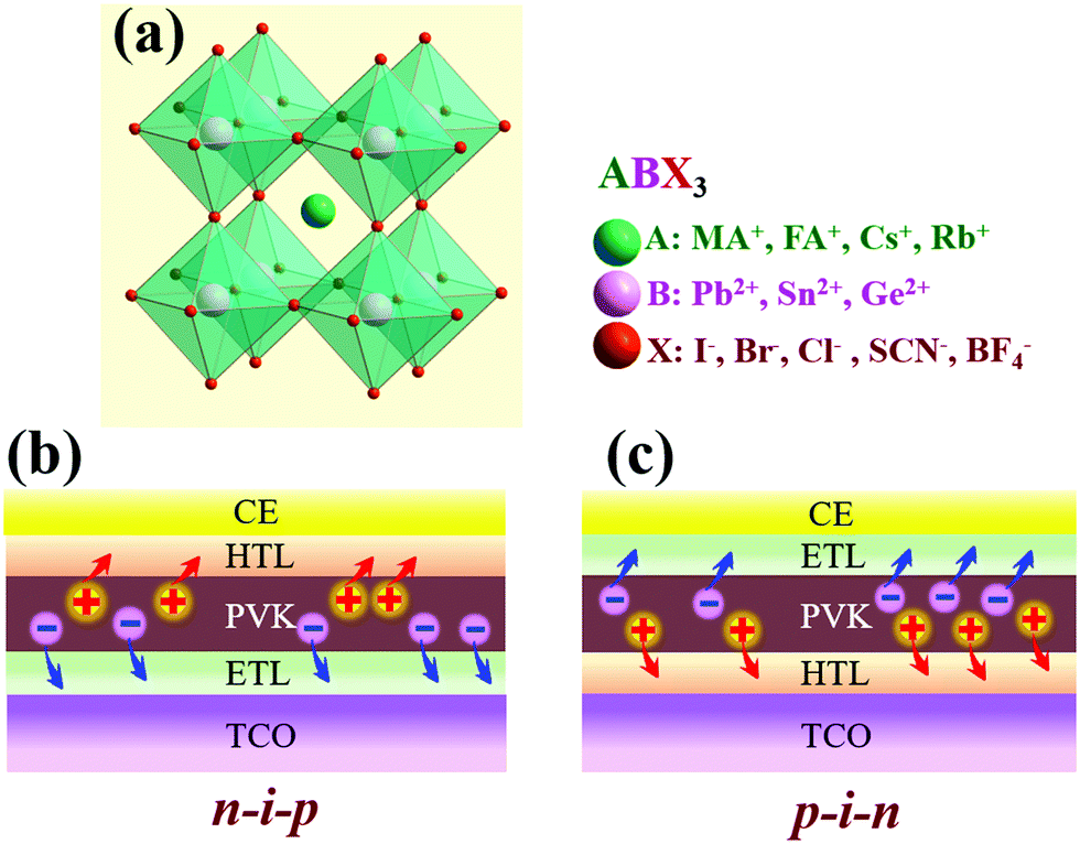 | ||
| Fig. 1 (a) Schematic diagram of the ABX3 perovskite crystal structure and the indication of compositional elements and groups for A, B and X. Structure diagram of the two predominant device geometries for conventional PSCs with (b) ETL/PVK/HTL n–i–p or (c) inverted HTL/PVK/ETL p–i–n structures. | ||
2.2 Theoretical basis of CTL-free PSCs
The perovskite layer, which is mainly responsible for light harvesting, is regarded as one of the most important parts in determining the performance of PSCs. Beyond acting as an efficient light absorber, it has been proven that the perovskite material itself can efficiently transport charge carriers, laying a solid foundation for constructing high-performance optoelectronic devices.23,24 Accordingly, a great deal of research has been devoted to unveiling the photo-physical processes in lead halide perovskites and corresponding devices, including carrier generation, transport to contacts, diffusion and recombination, etc. (Fig. 2a).1,25–27 Furthermore, charge transport and recombination processes are strongly related to the intrinsic optoelectronic properties of perovskite materials, such as carrier concentration, trap position and density, carrier mobility, carrier lifetime and diffusion length.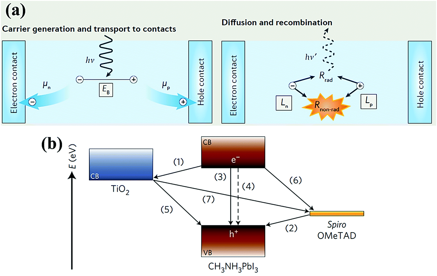 | ||
| Fig. 2 (a) Schematic diagram of the charge carrier dynamics in perovskite-based devices, such as carrier generation, transportation, diffusion and recombination.1 Reproduced from ref. 1 with permission from Springer Nature, copyright 2016. (b) Schematic illustration of the energy levels, as well as charge transfer and recombination processes in PSCs employing the conventional TiO2/MAPbI3/spiro-OMeTAD structure.28 Reproduced from ref. 28 with permission from Springer Nature, copyright 2014. | ||
Upon light illumination of a PSC, free carriers (i.e., electrons and holes) together with excitons will be generated and separated in the perovskite layer. Then the carriers diffuse across the perovskite layer to the perovskite/CTL interface. This gives rise to subsequent competition between interfacial charge injection and recombination, and only the survivors can be extracted by the CTL. To date, time-resolved ultrafast spectroscopy and electrical property measurements (e.g., transient laser spectroscopy, transient absorption and transient microwave photoconductivity measurements, etc.) have been conducted to quantify the time scale of different carrier dynamic processes within PSCs, which is of paramount importance for understanding the fundamental photo-physical processes, namely, photo-induced charge transfer and recombination that occur in an operational PSC device.
Taking the stereotyped TiO2/MAPbI3/spiro-OMeTAD structure as an example, there are at least seven routes for charge transport and recombination within the bulk perovskite layer and related interfaces (Fig. 2b).28 First, the free carriers and excitons (a ratio of 10![[thin space (1/6-em)]](https://www.rsc.org/images/entities/char_2009.gif) :1) can be excited and generated within picoseconds (<2 ps).29,30 It was reported that the exciton in MAPbI3 is assigned to the Wannier–Mott type with a weak binding energy of approximately 20–30 meV, which is comparable to the thermal energy kBT (kB is the Boltzmann constant and T is the temperature) of 26 meV and thus readily dissociates into free carriers at room temperature. A time scale of ∼20 fs has been observed for an ultrafast dissociation process from localized hot excitons to free carriers.31 This finding suggests that an ETL or HTL is not necessary to form a heterojunction with the perovskite layer for the purpose of facilitating exciton dissociation at the interface.32,33 The photo-generated carriers need to diffuse and travel across the perovskite layer before extraction by the CTL contact (routes 1 and 6). This diffusion process is largely dependent on the carrier diffusion length (Ln) of the perovskite material, which is a key parameter to evaluate the charge transport capability of the perovskite. Specifically, Ln can be calculated as Ln = (Dnτn)1/2, where Dn is the carrier diffusion coefficient defined as Dn = μq/kBT (q is the elementary charge and μ is the mobility), and τn is the recombination lifetime. Clearly, the diffusion length is determined by the carrier mobility and recombination lifetime of the perovskite material, which is related to its composition. For instance, Snaith and co-workers reported a long diffusion length exceeding 1 μm for a MAPbI3−xClx mixed halide perovskite thin film, which was an order of magnitude greater than that of its MAPbI3-based counterpart (∼100 nm).23 Our group reported that the mixed cation MA0.45FA0.55PbI3 perovskite single crystal exhibited a vastly longer diffusion length of 254 μm, together with an enhanced carrier mobility of 270 cm2 V−1 s−1, compared to both MAPbI3 (a Ln of 115 μm and a μ of 65 cm2 V−1 s−1) and FAPbI3 (a Ln of 118 μm and a μ of 150 cm2 V−1 s−1).34 Recent results have shown that mixed cation and halide perovskites with prolonged diffusion lengths are beneficial to further improving the device performance owing to their superior charge transport properties.
:1) can be excited and generated within picoseconds (<2 ps).29,30 It was reported that the exciton in MAPbI3 is assigned to the Wannier–Mott type with a weak binding energy of approximately 20–30 meV, which is comparable to the thermal energy kBT (kB is the Boltzmann constant and T is the temperature) of 26 meV and thus readily dissociates into free carriers at room temperature. A time scale of ∼20 fs has been observed for an ultrafast dissociation process from localized hot excitons to free carriers.31 This finding suggests that an ETL or HTL is not necessary to form a heterojunction with the perovskite layer for the purpose of facilitating exciton dissociation at the interface.32,33 The photo-generated carriers need to diffuse and travel across the perovskite layer before extraction by the CTL contact (routes 1 and 6). This diffusion process is largely dependent on the carrier diffusion length (Ln) of the perovskite material, which is a key parameter to evaluate the charge transport capability of the perovskite. Specifically, Ln can be calculated as Ln = (Dnτn)1/2, where Dn is the carrier diffusion coefficient defined as Dn = μq/kBT (q is the elementary charge and μ is the mobility), and τn is the recombination lifetime. Clearly, the diffusion length is determined by the carrier mobility and recombination lifetime of the perovskite material, which is related to its composition. For instance, Snaith and co-workers reported a long diffusion length exceeding 1 μm for a MAPbI3−xClx mixed halide perovskite thin film, which was an order of magnitude greater than that of its MAPbI3-based counterpart (∼100 nm).23 Our group reported that the mixed cation MA0.45FA0.55PbI3 perovskite single crystal exhibited a vastly longer diffusion length of 254 μm, together with an enhanced carrier mobility of 270 cm2 V−1 s−1, compared to both MAPbI3 (a Ln of 115 μm and a μ of 65 cm2 V−1 s−1) and FAPbI3 (a Ln of 118 μm and a μ of 150 cm2 V−1 s−1).34 Recent results have shown that mixed cation and halide perovskites with prolonged diffusion lengths are beneficial to further improving the device performance owing to their superior charge transport properties.
Simultaneously with the carrier generation and transfer processes, undesired charge recombination within the bulk perovskite layer and related interfaces occurs. For instance, intrinsic electron–hole pair recombination and the trap-assisted recombination in bulk perovskite films (routes 3 and 4, at a time scale of nanoseconds) severely compete with the charge transfer process. It is believed that trap-assisted (non-radiative) charge recombination results in VOC loss and is adverse to device performance. In general, passivation or elimination of these defects or trap states in bulk perovskite films is of critical significance toward high-performance PSCs.35,36 Additionally, for the so-called “back reaction” at related interfaces, i.e. the ETL/perovskite interface, there is a chance that the photo-injected electrons will further recombine with the holes in the perovskite or HTL (routes 5 and 7). Furthermore, the injected carriers will be possibly quenched by the surface trap states existing in the CTLs (routes 2 and 5, in microseconds). These adverse recombination processes can severely spoil the device performance of PSCs by lowering the JSC, VOC and FF. It is worth pointing out that both the TiO2/MAPbI3 and MAPbI3/spiro-OMeTAD interfaces witness a rapid charge transfer process with a timescale of ∼3 ps (routes 1 and 6), which is dramatically faster than that of the interfacial charge recombination process (routes 2 and 5) that occurs on a microsecond timescale (i.e., 15 μs and 99 μs at the ETL/perovskite and perovskite/HTL interfaces, respectively). Compared with the slower, nano- to microsecond-scale carrier recombination process at a nanosecond or even a microsecond-scale, the faster picosecond carrier generation, injection and transport processes emphasize the importance of employing both the ETL and HTL for rapid, efficient charge separation and extraction, thus suppressing interfacial charge recombination and achieving high device performance. This result imposes a great challenge of constructing high-performance CTL-free PSCs owing to severe and dominant interfacial charge recombination. However, success may be found by letting the charge transport process outcompete the interfacial charge recombination process. Encouragingly, Snaith and co-workers have demonstrated that charge collection in insulating Al2O3-based devices is more efficient than in the electron-injecting TiO2-based counterparts, indicating that the perovskite material itself is even more efficient in transporting electrons than the TiO2 ETL.24 This exciting finding has opened a new era in the research of perovskite materials and devices, which make PSCs feasible and versatile in diverse device architectures, especially emerging CTL-free PSCs with simplified device structures.
Overall, perovskite materials enjoy multiple advantages, such as fast exciton dissociation, high absorption coefficients, ambipolar carrier transport and long charge diffusion lengths. First, excitons in the perovskite layer can be dissociated into free electrons and holes spontaneously in the absence of CTLs. Second, ambipolar carrier transport means the perovskite itself is capable of transporting electrons and holes simultaneously, which, to some extent, weakens the necessity of employing ETL or HTL layers. Finally, owing to excellent defect-tolerant capability, perovskite materials exhibit long carrier diffusion lengths and high carrier mobility, enabling the efficient transport of free electrons and holes through the thin perovskite film being collected by the contact electrode. Collectively, these aspects inform the solid theoretical basis to support the successful implementation of CTL-free PSCs.
2.3 Structures and working principles of CTL-free PSCs
The development of CTL-free PSCs provides an “out-of-the-box” solution to reduce fabrication costs while simultaneously maintaining high efficiencies. In general, CTL-free PSCs can be classified into three categories, ETL-free, HTL-free and both ETL- and HTL-free, which are schematically illustrated in Fig. 3a. The underlying working mechanisms of the different types of CTL-free PSCs are dependent on the device geometries, interfaces and heterojunctions. For the n–i–p structured ETL-free device or the p–i–n structured HTL-free device, the first priority is the energy level alignment between TCO and the perovskite layer. In this case, the work function of the TCO (e.g. FTO, ITO or AZO) should match the energy level (i.e. conduction band (CB) or valence band (VB)) of the perovskite, which facilitates the extraction of one type of carrier while simultaneously blocking the transfer of another type of free carrier. In addition, it is anticipated that a metal–semiconductor contact is probably formed at the TCO/perovskite interface, which in some cases, provides a driving force for efficient charge transfer from the perovskite to TCO, provided favorable interfacial band bending occurs (Fig. 3b and c). In the case of n–i–p structured HTL-free PSCs, the driving force for the charge separation and transfer originates from the formation of the ETL/perovskite n–p heterojunction, which generates a beneficial depletion region at the interface. The resultant built-in potential can efficiently boost charge separation and extraction, as well as effectively suppress the back reaction of charge recombination (Fig. 3d). The depletion width at the ETL/perovskite interface is highly dependent on the ETL thickness, which is critical to controlling the carrier dynamics. For instance, an optimized depletion width of 395 nm for an approximately 620 nm thick TiO2 ETL leads to a champion PCE of 7.2% for a HTL-free PSC with a FTO/c-TiO2/m-TiO2/MAPbI3/Au structure.37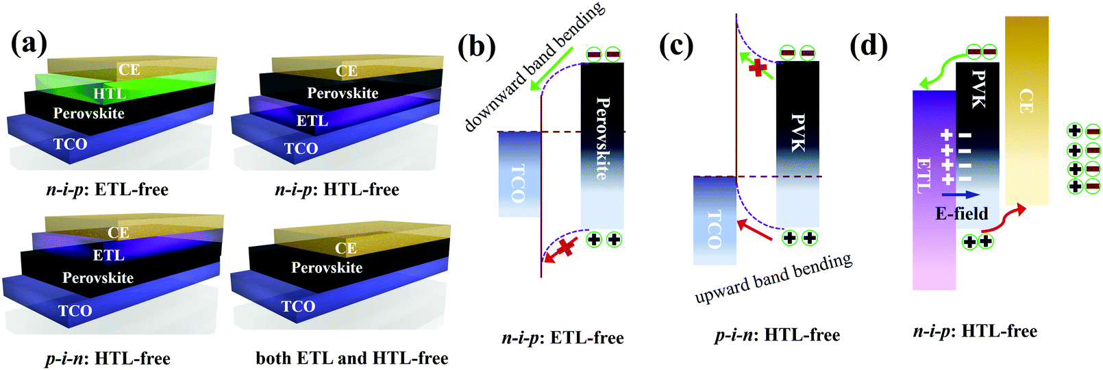 | ||
| Fig. 3 (a) Schematic illustration of the different representative CTL-free PSCs, including n–i–p structured ETL-free and HTL-free devices, p–i–n structured HTL-free devices and both ETL and HTL-free devices. Sketch showing the working mechanisms for different types of CTL-free PSCs, for instance. (b) A downward band bending at the TCO/perovskite interface for facilitated electron extraction in an n–i–p structured ETL-free device or (c) an upward band bending at the TCO/perovskite interface for boosted hole collection in a p–i–n structured HTL-free device or (d) the formation of ETL/perovskite n–p heterojunctions with a built-in electric field (E-field) for facilitated charge separation in n–i–p structured HTL-free PSCs. | ||
2.4 Current status of CTL-free PSCs
Despite increasing efforts, the currently reported PCEs of CTL-free PSCs still lag far behind those of conventional PSCs with CTLs. The reported PCEs for different types of CTL-free PSCs are compared in Fig. 4a. Unlike the conventional PSC with a record PCE of up to 25.2%, only a few ETL-free or HTL-free PSCs have achieved PCEs over 20% (Fig. 4b and c). Also, the development of both ETL and HTL-free PSCs still lags behind, despite being the simplest device structure (Fig. 4d). It is noticeable that the currently reported CTL-free PSCs are all fabricated on a lab-scale and small-area manner. The large-area demonstration of CTL-free PSCs is yet to be reported. This is mainly because the CTL-free device requires the highest standard of uniform perovskite film coverage on the underlying TCO substrate, otherwise, even a small pin-hole will result in device shunting and will be highly detrimental to the device performance. Besides, the operational mechanism is still unclear, and a fundamental understanding of the carrier dynamics, heterojunction merits and underlying device physics of the high-performance CTL-free PSCs is still lacking. Even though the study of CTL-free PSCs is still in its initial stages and the currently reported performances are still far from optimized, the great promise of commercializing high efficiency PSCs on the large-scale and in a cost-effective manner is undeniable and worthy of continued scientific efforts.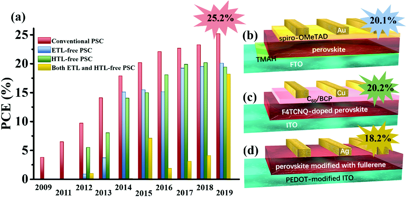 | ||
| Fig. 4 (a) Summary of the efficiency evolution of CTL-free PSCs with different device architectures. Schematic illustrations of the currently reported CTL-free device structures with record efficiencies: (b) ETL-free (TMAH-modified FTO/perovskite/spiro-OMeTAD/Au), (c) HTL-free (ITO/F4TCNQ-doped perovskite/C60/BCP/Cu) and (d) both ETL and HTL-free PSCs (ultra-thin PEDOT (1.6 nm)-modified ITO/MAPbI3−xClx modified with island-like fullerene (1 nm)/Ag). | ||
2.5 Limiting factors for CTL-free PSCs
Further improvement of the device performance of CTL-free PSCs is limited by several aspects, including insufficient surface coverage and uniformity, low-quality perovskite films with inferior carrier mobility, short diffusion length, high defect densities, mismatched energy level alignment and small built-in potential between the TCO and perovskite. These limiting factors are summarized: (1) direct deposition of perovskite films on pristine TCO substrates usually results in poor surface coverage and low uniformity with some amounts of pin holes due to either rough surface or hydrophobicity of the TCO substrate. This may result in the direct contact between TCO and other functional layers, thus causing device shunting and/or low device performance. (2) The polycrystalline perovskite films inevitably contain a high density of crystallographic defects, such as uncoordinated ions and dangling bonds at surfaces and grain boundaries, which can result in charge recombination via non-radiative channels, especially when the charges cannot be efficiently extracted out in the absence of CTLs, thus impairing the device performance. (3) In the absence of a CTL, the mismatched energy levels/work functions between TCO and the perovskite will cause significant interfacial recombination loss. This reduces efficiency owing to both electrons and holes migrating to the TCO/perovskite interface and recombining, leading to serious interfacial charge recombination and thus inferior charge collection. In addition, the perovskite may form an ohmic contact with the conductive TCO or metal electrode, which is less efficient at charge collection compared to the Schottky junction formed at the conventional CTL/perovskite interface. (4) The heterojunction formed at the TCO/perovskite interface normally does not have sufficient depletion width and built-in potential, thus lacking enough driving force to facilitate charge separation and extraction at the interface. (5) Upon front-side illumination, charge carriers are mainly generated at the TCO/perovskite interface. The photo-generated carriers must travel a long distance across the perovskite layer and reach the other side before being collected. Inferior charge collection is largely limited by the short diffusion length or insufficient carrier mobility (i.e. low crystallinity) of the commonly employed polycrystalline perovskite film, e.g. a diffusion length of only ∼100 nm for MAPbI3, much shorter than the film thickness (normally >500 nm). In this case, some photo-generated carriers may possibly recombine with other types of free carrier or become immobilized by numerous traps/defects in the bulk perovskite film before transporting to the interface. Overall, the under-optimized contacts for CTL-free devices are believed to dominate VOC and PCE losses, which hinder their potential to reach the Shockley–Queisser efficiency limit of 33.5%.383. Strategies for achieving high-performance CTL-free PSCs
In recent years, various strategies have been developed to improve the performance of CTL-free PSCs, such as TCO/electrode modification, perovskite morphology and composition optimization, bulk/interface heterojunction engineering, doping, device geometrical engineering and so on. In the following sections, progress of CTL-free PSCs by using different strategies is reviewed, with an emphasis on unveiling the fundamental carrier dynamics, heterojunction merits and device physics associated with different proposed models, and resolving controversies surrounding the competition between charge transport and recombination models. The pros and cons of different approaches are compared and evaluated, aiming at identifying the limitations of the proposed charge transport models, while also advancing some empirical models that could support the successful implementation of high-performance CTL-free PSCs.3.1 TCO/electrode modification
Most CTL-free PSCs, either n–i–p structured ETL-free devices or p–i–n structured HTL-free devices, are fabricated with perovskite films directly deposited on the bare TCO substrates. In the absence of the ETL or HTL, the photo-generated electrons or holes are expected to directly inject from the perovskite to TCO. The surface properties (e.g. work functions and wettability) and morphological characteristics (e.g. roughness and porosity) of TCO substrates are critical to determining the device performances of CTL-free PSCs. The first controversy over charge transport and recombination relates to which types of TCO substrates are suitable for CTL-free PSCs. Liu and co-workers systematically investigated the effects of different TCO substrates, fluorine-doped tin oxide (FTO), aluminum doped zinc oxide (AZO) and indium doped tin oxide (ITO), on the crystal growth of perovskite films, charge transport and recombination, as well as device performance of ETL-free PSCs. As expected, the three TCO substrates exhibited different work functions of −5.0 eV for FTO, −4.99 eV for AZO and −4.92 eV for ITO, thus incurring to different extents energy barriers for electron injection from the perovskite layer (Fig. 5a). In addition, the resultant perovskite films had different grain sizes, thicknesses and degrees of crystallinity when deposited on the different TCO substrates. Despite this diversity, similar device performances with PCEs of approximately 10% were achieved for all ETL-free PSCs, regardless of the different TCO substrates being employed.39 This result suggested that the choice of TCO substrates with only a small variation in work functions (i.e. <0.1 eV) has little effect on the device performance of ETL-free PSCs. Consequently, more focus should be put on TCO modification, aiming to improve the interfacial contact, optimize an interfacial energy level alignment, form the interfacial dipole between the perovskite and TCO for facilitated interfacial charge extraction and collection, and the suppression of charge recombination.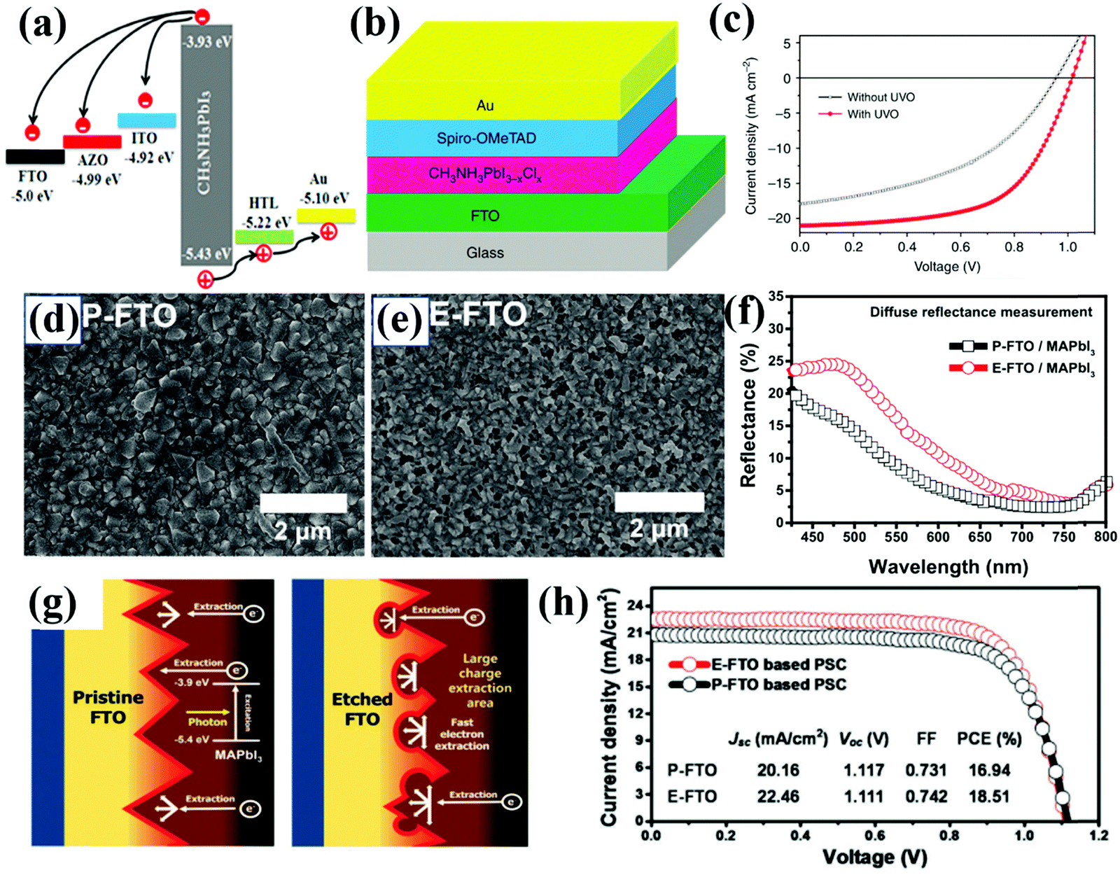 | ||
| Fig. 5 (a) Energy band diagram of the TCO/MAPbI3/HTL/Au device fabricated on different TCOs.39 Reproduced from ref. 39 with permission from Elsevier, copyright 2016. (b) Schematic view of the ETL-free PSC with a structure of FTO/MAPbI3−xClx/spiro-OMeTAD/Au and (c) J–V characteristics of ETL-free PSCs based on pristine FTO and UVO-treated FTO substrates.40 Reproduced from ref. 40 with permission from Springer Nature, copyright 2015. Surface SEM images of (d) pristine FTO (P-FTO) and (e) etched FTO (E-FTO). (f) UV-vis diffuse reflectance spectra for perovskite films deposited on different FTO substrates. (g) Schematic illustration of the charge extraction process from the perovskite to the P-FTO or E-FTO. (h) J–V curves of ETL-free PSCs fabricated on P-FTO or E-FTO substrates.42 Reproduced from ref. 42 with permission from John Wiley and Sons, copyright 2017. | ||
A uniform perovskite film with full surface coverage on a TCO substrate can, to a large extent, avoid device shunting, which benefits the fabrication of high-performance CTL-free PSCs. Yan and co-workers discovered that simple processing of a FTO substrate with ultraviolet ozone (UVO) treatment not only increased the wettability of the substrate (i.e. a decreased contact angle with DMF from 68.83° to 4.77°), but also removed residual organic species on the FTO substrates (Fig. 5b). The UVO-treated FTO substrates led to the formation of a high-quality MAPbI3−xClx perovskite film with improved smoothness and coverage, which inhibited direct contact between the FTO substrate and the HTL, yet improved interfacial contact at the perovskite/HTL interface for better hole extraction. Owing to the increased shunt resistance from 360 to 900 Ω cm2 and decreased series resistance from 7.19 to 3.90 Ω cm2, the ETL-free PSC had a superior PCE of 14.14%, which is higher than that of the control device fabricated on a pristine FTO substrate without UVO treatment (7.67%) (Fig. 5b and c). Notably, the PCE of the optimized ETL-free cell is comparable to that of a device with a TiO2 ETL (16.07%), proving that a TiO2 ETL is not indispensable for a high-performance PSC.40 Very recently, Chouhan and co-workers demonstrated that the reduction of superficial oxygen vacancies on an AZO surface via ozone treatment could result in a very thin doped region on top (6–9 nm). This induced favorable downward band bending at the TCO/perovskite interface, effectively facilitating carrier extraction while suppressing the back recombination with holes. As a result, the ETL-free PSCs based on the ozone-treated AZO substrate have an enhanced VOC of up to 1.05 V and significantly reduced J–V hysteresis.41
In addition to wettability, the roughness and/or morphology of the TCO substrate is crucial to the device performance of ETL-free PSCs. Inspired by the superior charge separation and extraction in mesoscopic structured PSCs owing to the enlarged interfacial contact between the perovskite and the mesoporous ETL, Jang and co-workers modified the surface of the FTO substrate to be porous via electrochemical etching, even though the pristine FTO substrate with a pyramid structure was already quite rough (Fig. 5d and e). The highly porous FTO substrate enhanced the scattering effect, thus boosting light capture (Fig. 5f). Significantly, the etched FTO increased the interfacial contact area between the perovskite and FTO, enabling fast charge extraction (Fig. 5g). As a result, the JSC was significantly improved from 20.16 to 22.26 mA cm−2, leading to an enhancement of PCE from 16.94% to 18.51% for ETL-free PSCs (Fig. 5h).42
Another benefit of TCO modification is to mitigate the mismatched energy level alignment between TCO and the perovskite. A common strategy is to deposit a thin layer of inorganic or organic materials on top of the TCO substrate, which can tune the surface work functions of the TCO, form an interfacial dipole and/or favorably influence the band bending direction at the TCO/perovskite interface for facilitated charge extraction and suppressed charge recombination. For instance, in the case of p–i–n structured HTL-free PSCs, there is a huge discrepancy between the work functions of TCO and the valence band maximum (VBM) of the perovskites, which leads to serious interfacial recombination, VOC loss, severe J–V hysteresis and ultimately instability in CTL-free PSCs. Gong and co-workers reported the surface modification of an ITO substrate with Cs2CO3; robust Cs–O bonding optimized the interfacial energy level alignment by up-shifting the work function of ITO upwards from −4.7 eV to −4.3 eV. The improved ohmic contact between the perovskite and ITO boosted electron extraction and collection at the TCO/perovskite interface (Fig. 6a and b). Surprisingly, the Cs2CO3-modified ITO itself could serve as an efficient electron-selective and hole-blocking contact, which enabled the fabrication of ETL-free PSCs with a PCE of 15.1% (Fig. 6c).43 Very recently, Ke and co-authors demonstrated that a surface modification agent, such as tetramethylammonium hydroxide (TMAH), can bond with FTO via N–O interactions. The TMAH modification up-shifted the work function of the FTO to form a dipole zone at the FTO/perovskite interface, which then favors interfacial electron transfer. In addition, unbound TMAH on the FTO surface helps facilitate the formation of highly crystalline perovskite films with reduced amounts of defects. Benefiting from the above-mentioned advantages, the PCE of the PSCs in the absence of ETLs has been elevated from 14.4% to 20.1% after TMAH surface modification, which is the highest reported value to date for the ETL-free PSCs.44 The concept of energy level matching between the TCO and perovskite has also been applied in inverted HTL-free PSCs. Very recently, Cheng and co-workers decorated an ITO surface with an organic monomolecular layer made of 4,4′-cyclohexylidenebis[N,N-bis(4-methylphenyl)benzenamine] (TAPC), which increased the work function of ITO and reduced the energy barrier for efficient hole extraction. In addition, the Sn–N bonding between TAPC and ITO fostered the formation of an interface dipole, which altered the band-bending direction at the ITO/perovskite interface from downward to upward (Fig. 6d–f), greatly enhancing the hole transfer from the perovskite to ITO. The presence of the interface dipole further enlarged the built-in potential, lifting the VOC from 0.75 V to 1.12 V and doubling the PCE of the HTL-free PSC from 10.26% to 19.42%. Additionally, the HTL-free PSC fabricated on TAPC-modified ITO showed significantly suppressed J–V hysteresis owing to the improved hole extraction efficiency at the ITO/perovskite interface (Fig. 6g).21
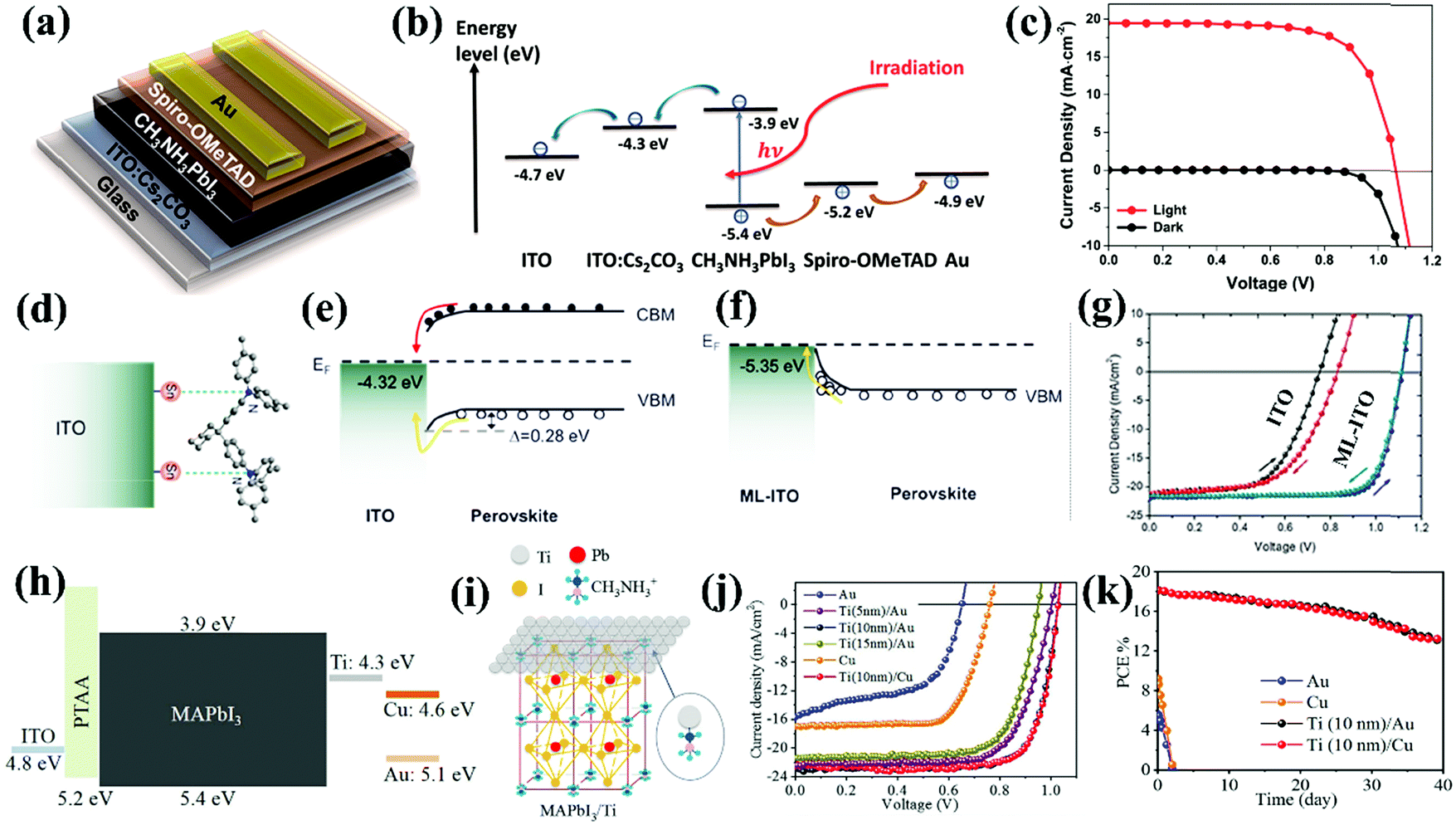 | ||
| Fig. 6 Schematic illustration of the (a) device structure and (b) energy level diagram of an ETL-free PSC based on Cs2CO3-modified ITO. (c) J–V curves of the ETL-free PSC fabricated on Cs2CO3-modified ITO substrates under one sun illumination and in the dark.43 Reproduced from ref. 43 with permission from American Chemical Society, copyright 2014. (d) Sketch showing the interaction of TAPC with the ITO substrate via the formation of Sn–N bonding. Charge transfer and extraction in HTL-free PSCs showing (e) downward band bending at the ITO/perovskite interface and (f) upward band bending at the metal liquid (ML)-ITO/perovskite interface. (g) J–V curves of HTL-free PSCs fabricated on ITO and ML-ITO measured under AM 1.5G one sun illumination in different scanning directions.21 Reproduced from ref. 21 with permission from American Chemical Society, copyright 2019. (h) Schematic energy level diagram of the ETL-free PSC employing a Ti interlayer. (i) Schematic illustration of the interaction between Ti and the MAPbI3 crystal structure. (j) J–V curves and (k) stability as a function of storage time in a N2-filled glove box (without encapsulation) of the inverted ETL-free PSCs based on different cathodes as indicated.53 Reproduced from ref. 53 with permission from John Wiley and Sons, copyright 2018. | ||
The conventional CTL-containing PSCs normally require a thin CTL with thickness >5 nm and sufficient surface coverage on the underlying substrate to avoid the direct contact of the perovskite layer with TCO or CE. Recently, Lunt et al. developed a very smart device structure design, where the ultrathin PEDOT and ultrathin incomplete fullerene layers are introduced to modify the TCO/perovskite and perovskite/CE interfaces. In their design, PEDOT is actually a TCO electrode material with metallic-like conduction. The incomplete layers of fullerene made of 1 nm islands of C60 are responsible for removing carrier barriers and enabling efficient carrier tunneling at the electrode interface, which makes this kind of device essentially a both HTL and ETL-free PSC.45,46 They comprehensively investigated the impact of the PEDOT thickness on the device performance of the corresponding PSC. Reducing the PEDOT thickness from 40 nm to 2 nm enabled the significant enhancement of the device performance up to 15%, accompanied by a decent VOC of 1.0 V, proving that the ultrathin PEDOT is able to eliminate the use of HTL, which showcases great potential to simplify the fabrication procedure and thus reduce the production cost.45 In the PSCs with an inverted p–i–n structure, the absence of fullerene ETL always resulted in poor PCE owing to the unfavorable electron injection at the perovskite/CE interface. In the follow-up work, the same group has introduced incomplete fullerene layers with only 1 nm islands of C60, which can modify the energy level alignment and guarantee efficient electron extraction from the perovskite to CE, thus suppressing the interfacial recombination. Combined with the aforementioned TCO and CE interfacial modification layers made of ultrathin (∼1.6 nm) PEDOT and ultrathin (∼1 nm) incomplete fullerene, an impressive PCE as high as 18.2% has been obtained for both HTL and ETL-free PSCs, which provides a new avenue for the future fulfillment of high-performance fully CTL-free PSCs.46
Overall, surface modification of the TCO substrate by introducing a thin non-CTL interlayer is promising for constructing ETL-free or HTL-free PSCs with high-performance; however, the complexity of device fabrication has not been sufficiently minimized, nor is the cost of materials or molecules currently explored. In addition, the thin layer is fabricated with a spin-coating technique, which is incompatible with large-scale manufacturing, unless this layer can be deposited via a rapid blade-coating or other self-assembly routes.
According to our experience and expertise, high-performance CTL-free PSCs should at least contain a favorable CTL/perovskite heterojunction on one side (or interface) to facilitate charge separation and extraction, thus suppressing charge recombination and minimizing the VOC loss. Similar to the modification of the TCO substrate, optimization of the remaining CTL and its related interface/heterojunction is equally important to ensure enhancement of device efficiency. Various researchers have demonstrated the use of submicron-sized TiO2 spheres,47 TiO2 nanosheets with exposed (001) facets,48 SnO2 or ZnO with high mobility as ETLs for constructing HTL-free PSCs,49 showing improved device performance as compared to TiO2 nanoparticle-based PSCs. For CTL/perovskite interface engineering, efforts such as introducing a self-assembled silane monolayer,50 an insulating Al2O3 layer51 or CsBr clusters52 have been reported. These interlayers play key roles in improving the interfacial contact between the CTL and the perovskite, passivating interface defects, forming an interface dipole and modifying the band alignment, leading to facilitated charge separation and extraction, retarded back reaction and suppressed interfacial charge recombination.
As a vital part of a monolithic PSC device, the CE which is either made of a noble metal or low-cost carbon is also worthy of optimization for achieving high-performance CTL-free PSCs. Xiao and co-workers modified the perovskite/cathode interface by introducing a Ti metal interlayer thereby avoiding the organic fullerene ETL commonly used in inverted PSCs. Ti has a work function of −4.3 eV that is close to the CB of the MAPbI3 perovskite (−3.9 eV), enabling electron transport while simultaneously blocking holes (Fig. 6h). It was found that a thermally evaporated Ti thin layer with a thickness of only ∼10 nm could form Ti–N bonding with the underlying perovskite layer, which not only passivated the surface defects of the perovskite layer, but also potentially retarded the degradation of the perovskite layer owing to ion immobilization (Fig. 6i). A PCE of up to 18.1% has been achieved for ETL-free PSCs with a structure of ITO/PTAA/perovskite/Ti/Au, which is significantly higher than those of their counterparts based on only an Au (5.6%) or Cu electrode (9.2%) without the Ti interlayer (Fig. 6j). Moreover, Ti efficiently inhibited the diffusion of metal atoms (Au or Cu) from the cathode into the perovskite layer, thus substantially improving device stability. As shown in Fig. 6k, the ETL-free devices using the Ti interlayer maintained nearly 90% of the original PCE after 15 days of storage in an N2-filled glove box without encapsulation, while performance degraded rapidly for the control devices without the Ti interlayer.53
3.2 Perovskite morphology optimization
It is generally believed that the morphology of the perovskite layer plays a crucial role in determining the device performance of PSCs.54,55 A great deal of effort has been invested in optimizing perovskite morphologies, which has led to the skyrocketing PCEs. The fabrication of a continuous, compact, smooth and flat perovskite film is a basic prerequisite towards high device performance. This requirement has become even more imperative in CTL-free devices, since even the presence of a small pinhole will raise the chances of current leakage or device shunting.Several reports have demonstrated that high-performance CTL-free PSCs are achievable as long as the resultant perovskite films are thick and dense enough to ensure efficient light absorption and block direct contact between the TCO and remaining CTL or between the TCO and CE owing to reduced shunting paths. High crystallinity, large grains and reduced defects are morphological bonuses. For instance, large grains are characterized by minimized grain boundaries, which corresponds to the reduction of surface defects and prolonged carrier lifetimes. Jang et al. investigated the effects of grain sizes and thicknesses of MAPbI3 perovskite films on the device performance of ETL-free PSCs. Grain sizes were enlarged from 200 nm to 1000 nm and the film thickness increased from 330 nm to 650 nm when the perovskite ink concentration was intentionally increased from 37 wt% to 58 wt%. In particular, the perovskite film prepared with the higher concentration of perovskite precursors featured dense packing of grains, in contrast to the observable pinholes in the film fabricated with lower ink concentration (Fig. 7a and b). As a result, the optimized ETL-free PSC based on a large-grain perovskite film delivered an improved PCE of 18.20%, accompanied by a JSC of 21.45 mA cm−2, a VOC of 1.127 V, and a FF of 0.751 (Fig. 7c). The large grain-based MAPbI3 film displayed an excellent blocking property, which inhibited the penetration of HTM through the perovskite film, further alleviating direct contact between the FTO and HTL. However, the penetration of a HTM through a small grain MAPbI3 film will cause severe charge recombination at the TCO/perovskite interface (Fig. 7d and e). Additionally, the smooth surface of the large grain-based MAPbI3 film is conductive to form a homogeneous interface with the HTL, which could facilitate interfacial hole extraction. Compared to a PSC with a TiO2 ETL, the ETL-free device exhibited stronger durability under ambient conditions, suggesting that elimination of the ETL improved device stability (Fig. 7f).56 Although a thick perovskite film is promising for constructing ETL-free PSCs, optimal film thickness should still be controlled, since too thick a perovskite film will hamper charge collection, thus impairing the device performance.
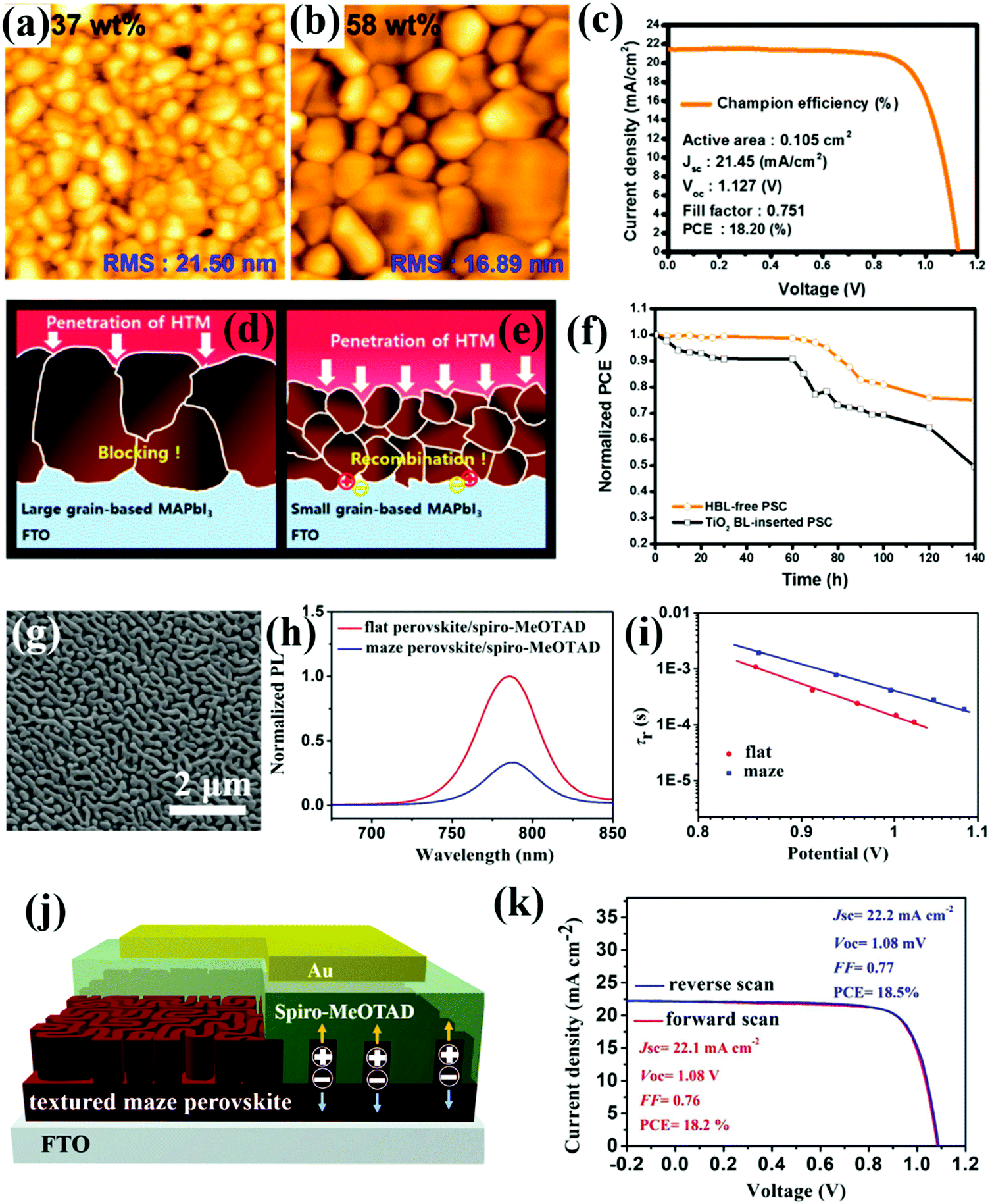 | ||
| Fig. 7 Surface AFM images of MAPbI3 films prepared by stock solutions with concentrations of (a) 37 wt% and (b) 58 wt%, respectively. (c) J–V curve of the champion cell based on large-grained perovskite films. Illustration depicting the penetration of the HTM and the behavior of charge recombination at the TCO/perovskite interface for (d) large-grain and dense perovskite films and (e) small-grain perovskite films with pinholes. (f) Long-term stability of the ETL-free or TiO2-inserted PSCs under ambient conditions (25 °C, 35% RH).56 Reproduced from ref. 56 with permission from American Chemical Society, copyright 2017. (g) SEM image of the maze-like MAPbI3 film. (h) PL spectra of the maze-like and flat perovskite films in contact with a spiro-OMeTAD layer. (i) Charge carrier lifetime as a function of voltage for the PSCs based on maze-like and flat perovskite films. (j) Schematic illustration of the charge separation and extraction in the ETL-free PSC based on a textured maze-like perovskite film. (k) J–V curves of the ETL-free PSC based on a maze-like perovskite film measured in reverse or forward scanning directions.57 Reproduced from ref. 57 with permission from John Wiley and Sons, copyright 2019. | ||
The rule for constructing a compact perovskite film with large grains for CTL-free PSCs is also applicable to other perovskite compositions, such as mixed cation and mixed halide perovskites or all-inorganic perovskites. The cesium-based all-inorganic perovskite has shown great potential to fabricate HTL-free PSCs in combination with a carbon electrode, owing to the matched energy level alignment within the device. However, unlike the well-developed techniques for depositing high-quality MAPbI3, the distinct solubility of CsX and PbX2 (X = Br, I) raw materials in organic solvents (e.g. DMF, DMSO) imposes a great challenge to preparing high-quality all-inorganic perovskite films on substrates. Typically, the CsPbX3 film prepared with a one-step spin-coating method normally suffers from inferior surface coverage and small grains, which provides numerous non-radiative channels for trap-assisted recombination and has even caused short-circuiting in the PSC device.58,59 Considerable effort has been made on enlarging the grain size, improving the surface coverage and enhancing the crystallinity of the all-inorganic perovskite films, for example by controlling the CsPbBr3 film crystallization kinetics by Sm3+ ion incorporation,60 surface reconstruction of the CsPbIBr2 film with CsI treatment,61 or a dual-source thermal evaporation of CsPbIBr2 perovskite films,62etc. Encouragingly, all-inorganic perovskite-based HTL-free PSCs have attained PCEs exceeding 10% via morphological optimization.
Distinguished from the conventional concept of constructing ETL-free PSCs by employing compact and dense perovskite films, a recent study demonstrated an “out-of-the-box” solution to simplify PSC device architectures by utilizing emerging textured perovskite morphology with a porous structure. Very recently, we fabricated a maze-like perovskite film through incorporating MACl as an additive (Fig. 7g) and applied it to fabricate ETL-free PSCs. The maze-like perovskite film is composed of a dense bottom layer and a porous top layer, which has shown exceptional promise to be used in ETL-free devices. Specifically, the dense bottom layer could prevent the possibility of direct contact between the HTL and TCO substrate. In contrast, the porous perovskite top layer could increase the interfacial contact with the HTL for facilitated charge separation and extraction, as is evidenced by dramatically quenched photoluminescence (PL) intensity compared to the flat perovskite (Fig. 7h). In this case, the photo-generated holes need only diffuse or travel through a very short distance before extraction by the CE, which could reduce the over-accumulation of free carriers at the TCO/perovskite interface and so suppress interfacial charge recombination, as indicated by the prolonged carrier lifetime (Fig. 7i) and high VOC of 1.08 V. Benefiting from accelerated charge separation and extraction at the HTL/perovskite interface, as well as suppressed interfacial charge recombination (Fig. 7j), the ETL-free PSC based on maze-like perovskite film had an impressive PCE of up to 18.5% and negligible J–V hysteresis (Fig. 7k).57 Considering that the textured perovskite morphology can facilitate charge separation and boost charge extraction to one side of a charge-selective contact, we believe it can be a versatile and powerful strategy to design other simplified device structures in HTL-free or both ETL- and HTL-free configuration optoelectronic devices. Similar to the textured perovskite film, it was reported that the presence of moderate amounts of pinholes in a perovskite film is good for accelerating charge separation. Very recently, Zhang and co-workers discovered the benign effect of pinholes in a CsPbIBr2 film, which would not form detrimental shunting paths when the film thickness increased from 340 nm to 710 nm. In the case of the thin CsPbIBr2 film, carbon paste completely permeated the pinholes, and directly contacted the TiO2 ETL. By contrast, the sticky nature of the carbon paste limits its penetration through the thick CsPbIBr2 film, preventing direct contact between the carbon and ETL, thus avoiding device shunting. In addition, the pinholes at the top surface of the perovskite layer effectively enlarge the contact area with the carbon, thus boosting charge separation and transfer. As a result, a PCE of 9.05% was achieved based on the CsPbIBr2 perovskite film, outperforming the pinhole-free counterpart (5.05%).63
3.3 Heterojunction engineering
A compromised yet practical strategy to simplify the fabrication process of PSCs while simultaneously retaining the functions of the CTL is to construct a perovskite–CTL bulk heterojunction (BHJ) via a co-deposition strategy. Wu and co-workers were the first to report a BHJ-based PSC by incorporating PCBM into perovskite films, which played a beneficial role in enhancing the device performance. Specifically, the incorporated PCBM can modulate the crystal growth and crystallization of the perovskite, inducing the growth of a more continuous and denser film with large grains and reduced defect densities, which retarded trap-assisted recombination. The perovskite–PCBM BHJ film exhibited much weaker PL emission than a pure perovskite film, because charge transfer from the perovskite to the PCBM quenched the PL, which suggested improved charge collection. In addition, a space-charge limited current (SCLC) study verified that the electron and hole mobility of the perovskite layer was significantly enhanced after the incorporation of 0.1 wt% PCBM into the perovskite films (Fig. 8a). As a proof-of-concept, an ETL-free PSC with a structure of ITO/PEDOT:PSS/MAPbI3 + 0.1 wt% PCBM BHJ/Ca/Al was created (Fig. 8b and c), yielding a PCE of 12.1%. This study presented a useful way to fabricate an ETL-free PSC via effective BHJ engineering.64 Very recently, Priya and co-workers discovered that introducing a polymethyl methacrylate (PMMA)–fullerene complex into the perovskite layer to form a BHJ not only facilitated charge extraction, but also enhanced the device stability. On the one hand, the incorporated fullerene promotes charge separation by forming a localized dipole-like electric field within the bulk perovskite layer, facilitating charge extraction and increasing the JSC. On the other hand, the hydrophobic PMMA distributed on the surface of the perovskite grains can effectively prevent incursion of molecular water, thus enhancing the device stability. As a result, the ETL-free PSC based on this PMMA–fullerene complex modified perovskite film achieved a PCE of 18.4% and superior stability for 250 days in ambient air (23–47% relative humidity).65 The concept of BHJ engineering has also been extended to HTL-free PSCs. Huang and co-workers mixed CuSCN HTMs into the perovskite precursor, which enabled the fabrication of inverted HTL-free PSCs (Fig. 8d). The introduced CuSCN not only passivated the defect grain boundaries of the perovskite, but also accelerated hole transfer from the perovskite to the ITO due to the better matched energy level between CuSCN (−5.3 eV) and the MAPbI3−xClx perovskite (−5.4 eV). Time-resolved photoluminescence (TRPL) revealed that the intensity decay of the ITO/MAPbI3−xClx (CuSCN) film was as fast as that of a glass/MAPbI3−xClx/C60 film, providing further evidence that the incorporation of CuSCN accelerates hole transfer and collection (Fig. 8e). In addition, the recombination resistance (Rrec) of the HTL-free PSC with CuSCN incorporated was much larger than that of the control device without CuSCN, meaning CuSCN was able to suppress charge recombination within the device even in the absence of a HTL. As a result, a more balanced charge (i.e. electrons and holes) transfer to the respective contact electrodes was realized, reducing the possibility of charge accumulation while charge recombination was suppressed, and yielded a PCE of 18.1% with negligible J–V hysteresis.66 In a follow-up work, the same group demonstrated incorporation of a novel p-type material Cu(thiourea)I [Cu(Tu)I] in the perovskite layer to form a BHJ, which enlarged the depletion width from 126 nm to 265 nm and thus boosted hole transfer. Additionally, the iodide in Cu(Tu)I can effectively alleviate halide vacancies by bonding with under-coordinated Pb cations. In particular, the incorporation of Cu(Tu)I diminished the trap state energy level of the perovskite from 0.35–0.45 eV to 0.25–0.35 eV, which effectively reduced the amount of trap densities and confirmed the beneficial role of Cu(Tu)I in defect passivation (Fig. 8f). Notably, Cu(Tu)I possesses an identical VBM to the perovskite, which completely eliminates potential wells for holes, facilitating hole extraction and suppressing charge recombination (Fig. 8g). Benefiting from these advantages, a PCE of 19.9% has been achieved for a HTL-free PSC employing the perovskite–Cu(Tu)I BHJ.67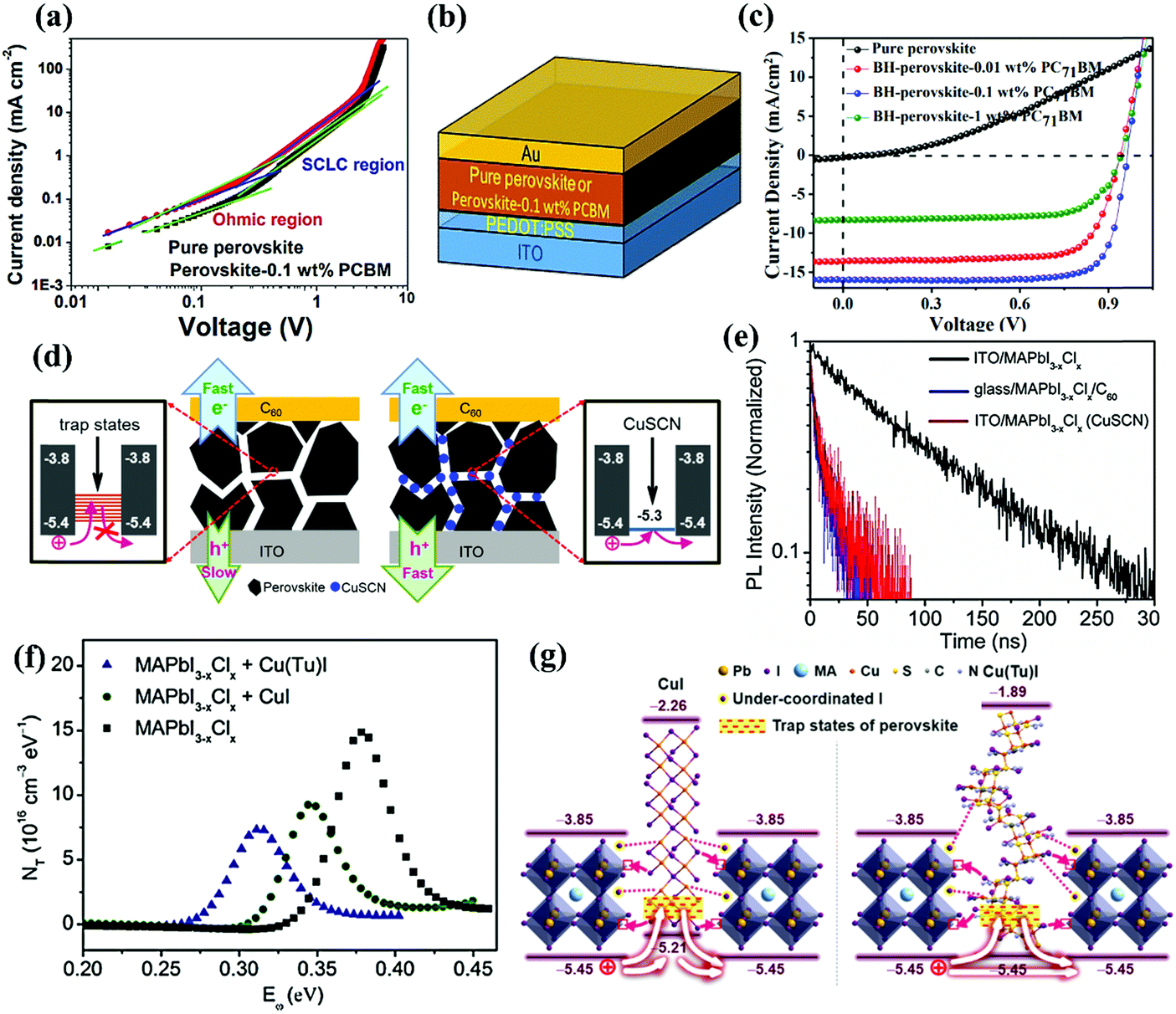 | ||
| Fig. 8 (a) Electron and hole mobility characterization of the perovskite–0.1 wt% PCBM BHJ film via a space-charge limited current (SCLC) test. (b) Device architecture of the inverted ETL-free PSC based on the perovskite–PCBM bulk heterojunction. (c) J–V curves of the inverted PSCs based on pure perovskite and perovskite–PCBM bulk heterojunction films with different PCBM contents.64 Reproduced from ref. 64 with permission from Springer Nature, copyright 2016. (d) Schematic illustration of the charge extraction and recombination processes in the devices with or without CuSCN incorporation. (e) Time-resolved photoluminescence (PL) decay of the ITO/MAPbI3−xClx, glass/MAPbI3−xClx/C60 and ITO/MAPbI3−xClx (CuSCN) films.66 Reproduced from ref. 66 with permission from John Wiley and Sons, copyright 2016. (f) Trap-state density (NT) of the PSCs based on MAPbI3−xClx, MAPbI3−xClx + CuI, MAPbI3−xClx + Cu(Tu)I. (g) Schematic illustration of the defect passivation and charge extraction mechanism for the perovskite with incorporated CuI or Cu(Tu)I.67 Reproduced from ref. 67 with permission from American Chemical Society, copyright 2017. | ||
Overall, direct incorporation of CTL materials into perovskite films to form a BHJ, which can modulate the crystal growth of perovskite film, passivate surface imperfections and facilitate charge extraction, is an ideal way to simplify the device structure while maintaining the high efficiency of CTL-free PSCs. Co-deposition is a promising strategy to reduce production costs and promote the practical application of CTL-free PSCs. However, the incorporated amounts of CTL materials should be carefully optimized, otherwise excess additives will in turn serve as recombination centers that will deteriorate the device performance. In addition, some CTL materials, especially inorganic candidates, exhibit poor solubility in perovskite ink, which limits the selection of alternative materials and narrows the scope for optimization.
Heterojunction engineering is not limited solely to the bulk; the concept can also be implemented in relevant interfaces, for instance, constructing an interfacial gradient heterojunction. Perovskite materials are much cheaper than the commonly used HTMs, such as spiro-OMeTAD. However, the elimination of the HTL in PSCs, more often than not, results in an unwanted electron flow to the CE, which will lead to severe charge recombination and performance degradation. Additionally, the absence of the HTL is always accompanied by inferior hole extraction, thus aggravating interfacial charge recombination and limiting the performance of HTL-free PSCs. In theory, the HTL can be replaced by another perovskite layer as long as its energy level is suitable, which favors cascade charge transfer. Yin and co-workers developed the concept of multi-graded-heterojunction (GHJ), featuring multi-layered inorganic perovskite CsPbBrxI3−x nanocrystal layers (i.e. CsPbI3, CsPbBr0.3I2.7, CsPbBr0.7I2.3) with gradient bandgap stacking onto the MAPbI3 (Fig. 9a). Via a rational halide composition tuning, an optimal energy level alignment between MAPbI3 and CsPbBrxI3−x has been achieved, which enabled a cascade hole extraction and conduction from MAPbI3 to the CE (Fig. 9b). The VBM offset between MAPbI3 and multiple CsPbBrxI3−x layers builds up a built-in electric field that provides a driving force to boost charge separation and extraction at the MAPbI3/CE interface. Specifically, the GHJ with three-grades showed the most efficient charge extraction, as characterized by the fastest TRPL decay (Fig. 9c). Additionally, the multiple layers of CsPbBrxI3−x achieved robust electron blocking, suppressing electron flow from the perovskite to the CE, in turn retarding the interfacial charge recombination. As a result, this well-designed three-grade MAPbI3–CsPbBrxI3−x GHJ enabled the construction of HTL-free PSCs with an improved PCE of 11.33%, compared to 8.16% based on pristine MAPbI3 (Fig. 9d). Introduced inorganic CsPbBrxI3−x multi-graded layers can effectively prevent the direct contact of MAPbI3 with permeating water molecules, and simultaneously enhance the thermal stability of the perovskite film (Fig. 9e).68 Very recently, Zhang and co-workers fabricated MAPbI3–MAPbIxBr3−x GHJ via an in situ reaction approach. Specifically, a layer of MABr was deposited onto the MAPbI3 surface to trigger in situ growth of a mixed-halide MAPbIxBr3−x thin layer (Fig. 9f), enabling the construction of a HTL-free PSC with a carbon CE directly deposited on top of the perovskite layer (Fig. 9g). Upon introduction of the MAPbIxBr3−x perovskite stacking layer, a faster PL decay was observed, suggesting that the photo-generated holes in the MAPbI3 layer can be efficiently extracted to the CE (Fig. 9h). Without modification, both photo-induced electrons and holes can transport to the carbon CE, and recombine there owing to the unfavorable energy level alignment between the MAPbI3 and carbon. In contrast, modification of the MAPbIxBr3−x layer on the surface can not only facilitate the hole extraction, but also block electron flow from the perovskite to the carbon CE (Fig. 9i). Such a GHJ modification has facilitated interfacial charge transport and suppressed interfacial charge recombination, thus contributing to an increased PCE from 11.3% to 16.2% with consistently high reproducibility, accompanied by a concurrent enhancement of the JSC from 18.9 to 20.8 mA cm−2 and FF from 0.60 to 0.73 (Fig. 9j).69 To our knowledge, this PCE is decent for carbon-based PSCs in the absence of a HTL.
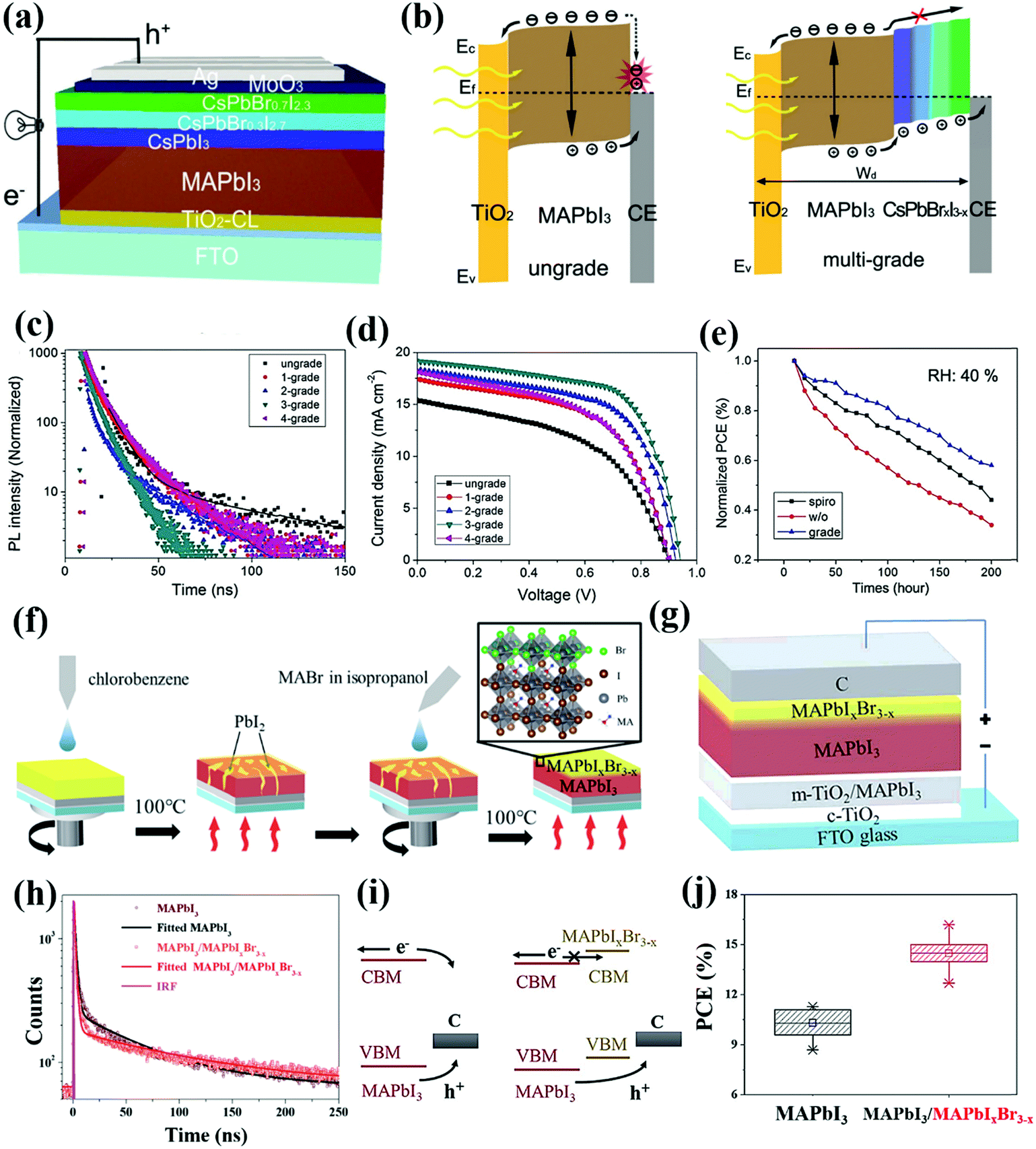 | ||
| Fig. 9 (a) Schematic illustration of the HTL-free PSC with multi-graded CsPbBrxI3−x films. (b) Sketch showing the charge transfer and recombination in the single grade or multi-grade HTL-free PSC. (c) TRPL spectra of semi-devices fabricated with MAPbI3, graded NC and Ag films. (d) J–V curves of the HTL-free PSCs based on single grade or multi-grade perovskite films. (e) Normalized PCE variation of PSCs stored under 40% humidity at room temperature.68 Reproduced from ref. 68 with permission from John Wiley and Sons, copyright 2017. (f) Schematic of the in situ reaction growth of a MAPbIxBr3−x thin layer on top of a pristine MAPbI3 layer. (g) Device structure of the HTL-free PSC based on MAPbI3/MAPbIxBr3−x GHJ. (h) TRPL decay of the MAPbI3 and MAPbI3/MAPbIxBr3−x perovskite films. (i) Illustration of the charge transfer at the MAPbI3/C interface and MAPbI3/MAPbIxBr3−x/C interface. (j) Statistical PCEs for the HTL-free PSCs based on the MAPbI3 or MAPbI3/MAPbIxBr3−x perovskite films.60 Reproduced from ref. 60 with permission from Royal Society of Chemistry, copyright 2019. | ||
Overall, the concept of GHJ provides an innovative route to fabricate CTL-free PSCs. Essentially, the perovskite layers with gradient bandgaps mainly serve as HTLs owing to suitable energy levels between the perovskite and the CE. Hence, this strategy holds promise for fabricating HTL-free PSCs, since most perovskite materials are found to be more efficient in conducting holes. Positive aspects of this strategy are a tunable bandgap, low cost and relatively better stability of the perovskite materials, which afford diverse possibilities to simplify the device structures and avoid the use of expensive and unstable CTL materials. Yet the GHL strategy also has negative aspects. For instance, unlike a HTL with specific energy levels and designated conductivity, the GHJ requires multiple layer-stacking between the perovskite and the CE, which not only makes the fabrication procedure complicated, but also increases the series resistance for charge transfer owing to the existence of multiple interfaces. We anticipate that this dilemma can be overcome if the offset between the VB of the perovskite and the work function of the CE are minimized, or a similar doping strategy can be applied to GHJ multi-graded perovskite layers like that for HTLs.
3.4 Carrier dynamics tuning via composition engineering or doping
As mentioned above, working CTL-free PSCs should at least contain one p–n junction that can facilitate charge separation and extraction. Although perovskite materials are capable of ambipolar charge transfer, severe carrier recombination remains a major concern in the absence of CTLs, because there is no preferred direction for carrier transport in the bulk perovskite film. In this case, the device performances of the CTL-free PSCs will be strongly related to whether the photo-generated carriers survive traveling long distances across the whole perovskite film to be collected by the electrode. The carrier dynamics are dominated by the carrier mobility, lifetime, diffusion length and doping levels of the perovskite materials. Controlling the carrier dynamics is of great importance to improving the device performance of CTL-free PSCs. The perovskite material, i.e., MAPbI3, is reported to have a self-doping property, which can be easily achieved by tailoring the composition stoichiometry, namely, the PbI2 and MAI ratio. Cui and co-workers realized the composition management of MAPbI3 perovskites by increasing the annealing temperature from 60 °C to 150 °C, which gradually shifted the Fermi level upwards and changed the doping levels from p-type to n-type (Fig. 10a and b). It is proposed that the doping feature of perovskite films originates from a change in the defect states. In this scenario, the high annealing temperature is believed to remove excess MAI while reducing the Pb vacancies and/or I interstitials. As a result, an n–p heterojunction was spontaneously formed at the heavily n-doped MAPbI3/p-type spiro-OMeTAD interface, which efficiently boosted charge separation and extraction, suppressing the charge recombination, and enabling the fabrication of an ETL-free PSC with a PCE of 15.69%.16,70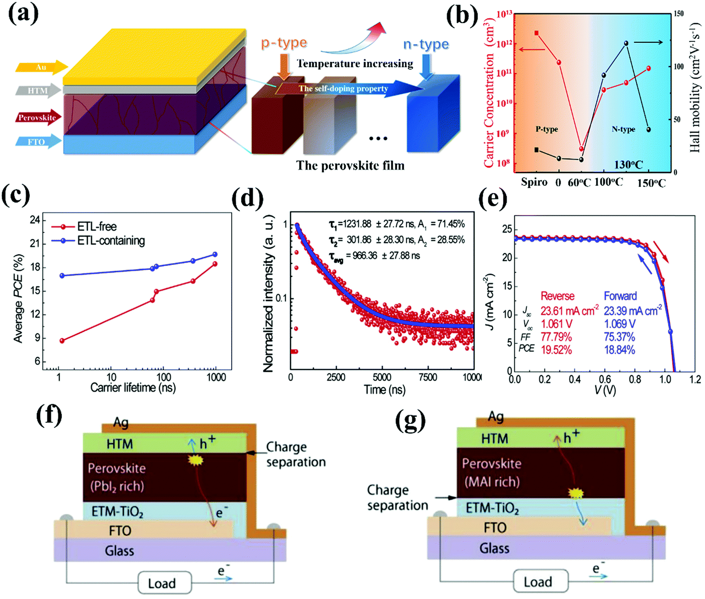 | ||
| Fig. 10 (a) Device architecture of the n–i–p structured ETL-free PSC, and illustration of the self-doping property of the perovskite film showing the change from p-type to n-type due to the increasing annealing temperature. (b) Annealing temperature dependent carrier concentration (red) and carrier mobility (black) in perovskite films (circle) and the spiro-OMeTAD film (square) by Hall measurements.70 Reproduced from ref. 70 with permission from John Wiley and Sons, copyright 2019. (c) Correlations between the carrier lifetimes of perovskite films and average PCE for both ETL-free and ETL-containing PSCs. (d) TRPL spectrum of a FA0.83Cs0.17Pb(I0.6Br0.4)3 perovskite film. (e) J–V characteristics of an ETL-free PSC device based on the FA0.83Cs0.17Pb(I0.6Br0.4)3 perovskite film with 5% excess PbI2 measured under AM 1.5G one sun illumination in different scanning directions.71 Reproduced from ref. 71 with permission from Elsevier, copyright 2018. Schematic of charge separation: at the (f) perovskite/HTL interface for a PSC based on a PbI2-rich perovskite film and (g) ETL/perovskite interface for a PSC based on a MAI-rich perovskite film.72 Reproduced from ref. 72 with permission from Springer Nature, copyright 2019. | ||
The carrier lifetime of the perovskite material is another important factor determining the device performances of CTL-free PSCs. Very recently, Hu and co-workers demonstrated that prolonging carrier lifetimes in the perovskite films can facilitate charge collection efficiency and enhance device performance in ETL-free PSCs (Fig. 10c). The prolonged carrier lifetime was realized by intentionally introducing excess PbI2 into the pristine perovskite composition. In addition, the carrier lifetime is quite sensitive to the perovskite compositions. The mixed cations and mixed halides, FA0.83Cs0.17Pb(I0.6Br0.4)3, exhibited a much longer carrier lifetime than the MAPbI3 counterpart (966 ns and 1.71 ns, respectively) (Fig. 10d). A longer carrier lifetime is beneficial for the higher device efficiency of ETL-free PSCs. For the ETL-free device based on FA0.83Cs0.17Pb(I0.6Br0.4)3 with 5% excess PbI2, the engineered carrier lifetime is approaching 1 μs. This resulted in a PCE of 19.5% with reduced hysteresis (Fig. 10e), and the performance was comparable to that of an ETL-containing PSC. Interestingly, the excess PbI2 only increased the carrier lifetime of the perovskite, and did not boost the electron injection rate at the ITO/MAPbI3 interface.47 This discovery indicated that the carrier lifetime is the key determining factor to achieve high-efficiency n–i–p structured ETL-free PSCs, rather than the efficacy of the electron extraction at the TCO/perovskite interface. This is quite reasonable, since there is already energy level alignment between ITO and pristine MAPbI3, which favors electron injection and extraction. Han and co-workers also discovered that the composition stoichiometry of the perovskite can affect the diode junction formed at different interfaces. For instance, excess PbI2, acting as an n-type dopant, could shift the diode junction to perovskite/HTL interface (Fig. 10f). In this case, the PbI2-rich perovskite film is conductive enough to form an efficient n–p heterojunction with the HTL for facilitated charge separation and extraction. This discovery, to an extent, explains why the electron-injection rate at the ITO/MAPbI3 interface was not changed in the presence of excess PbI2. To make an efficient ETL-free PSC, one should only consider enhancing the electron lifetime and/or mobility, which ensures that photo-generated electrons can travel rapidly through the perovskite film to be collected by the TCO in the absence of an ETL. Alternatively, excess MAI could increase the hole concentration, thus enabling p-doping of the perovskite and formation of an n–p junction at the ETL/perovskite interface.72 We anticipate that modulating the formation of diode junctions at different interfaces via tailoring the perovskite stoichiometry will be a versatile strategy to construct efficient CTL-free PSCs, namely, excess PbI2 for ETL-free devices and excess MAI for HTL-free devices (Fig. 10g). However, introducing too many raw materials will inevitably bring about additional charge recombination centers, which would be detrimental to device performance and adverse for the long-term stability of CTL-free PSCs. The necessity of forming a robust p–n junction to enhance the device performance of PSCs has been verified by other works. For instance, Luther and co-workers fabricated bi-layered Cs0.25FA0.75PbI3/CsPbI3 perovskite quantum dot (QD)-based films with abrupt compositional changes. This layer stacking of perovskite QDs with different compositions induced an internal p–n heterojunction, which efficiently facilitated the charge separation to achieve enhanced photo-carrier harvesting. The pristine Cs0.25FA0.75PbI3 films witnessed the trade-off between long free-carrier lifetimes and low effective mobility, which led to severe charge recombination. Fortunately, this drawback was overcome by introducing an additional CsPbI3 layer with superior mobility. This ingenious p–n junction engineering led to the fabrication of high-performance perovskite QD-based solar cells with a PCE of up to 17.39%.73 Very recently, Li and co-workers proposed the novel concept of a p–n homojunction, which formed in the perovskite film via stacking of a thermally evaporated, MAI-rich, p-type perovskite layer onto a solution-processed, PbI2-rich, n-type perovskite layer. The p–n homojunction generated a built-in electric field, which provided a strong driving force to promote the oriented, directional transport of photo-generated carriers within the bulk perovskite layer, thus effectively reducing carrier recombination losses. The rates of carrier generation were almost the same for both the standard p–i–n PSC and the homojunction PSC, whereas the carrier recombination rate for the p–n homojunction-based PSCs was dramatically reduced near the interface between the p-type and n-type perovskites owing to facilitated charge separation. Unsurprisingly, such a robust p–n homojunction enabled the construction of a simplified PSC in the absence of both ETL and HTL, yielding a PCE of over 8%, which is the highest reported value for PSCs with the simplest device structure without using any interfacial modification layers.74
Apart from the formation of p–n heterojunctions or homojunctions for facilitated charge separation and extraction, one should also tune the carrier dynamics by selecting appropriate perovskite compositions. Fig. 12 depicts the energy levels of perovskites of various compositions, TCOs, CTLs and CEs, providing a graphical overview to guide the selection of perovskite materials for efficient CTL-free PSCs. This is accompanied by a summary of the key charge-carrier properties of perovskites with different compositions (Table 1). Besides the commonly used MAPbI3, other perovskite compositions, such as mixed cation and mixed halide perovskites and all-inorganic perovskites have been explored for CTL-free PSCs. In general, for the ABX3 structured perovskite, changing the A site cation will affect the crystal structure and bandgap owing to the lattice expansion/contraction or PbX6 cage tilting, while altering the B site metal cation or X site halide anion will significantly affect the carrier dynamics (carrier mobility, diffusion length, etc.) of the perovskite materials. For instance, by replacing some portion of I with Cl, the MAPbI3−xClx perovskite exhibited higher carrier diffusion coefficients (0.042 cm2 s−1 for electrons and 0.054 cm2 s−1 for holes) and longer electron–hole diffusion length (1069 nm for electrons and 1213 nm for holes) than that of the MAPbI3 counterpart (129 nm for electrons and 105 nm for holes).23 It is anticipated that MAPbI3−xClx is more suitable for use in CTL-free PSCs with a planar device architecture. Recently, Han and co-workers replaced the I− with BF4− owing to the similar ionic radius between these two anions (i.e. 0.220 nm for I− and 0.218 nm for BF4−). Compared to the pristine MAPbI3, the MAPbI3−x(BF4)x becomes more p-type, showing remarkably enhanced hole mobility, and a device performance improvement from 10.54% to 13.24% for HTL-free PSCs.75 Tang and co-workers demonstrated the incorporation of lanthanide ions into the CsPbBr3 perovskite composition, which significantly reduced defects while prolonging the carrier lifetimes. As a result, the Sm3+ incorporated CsPbBr3-based, HTL-free PSC achieved a PCE of over 10%, accompanied by a high VOC of 1.594 V (corresponding to a VOC deficit of 0.7 V) and an extremely high FF of 0.851.60 This PSC without using a CTL annealed at high temperature shows the potential for full implementation of the low temperature fabrication, thus being compatible with flexible substrates. Yang and co-workers directly deposited a uniform and compact chlorine-incorporated CH(NH2)2PbI3 (Cl-FAPbI3) layer onto an ITO/polyethylene naphthalate (PET) flexible substrate, achieving a PCE of 12.70% for the flexible ETL-free PSC. This decent device performance can be attributed to heterojunction merits within the devices, in which the charge accumulation in the Cl-FAPbI3 perovskite layer results from the gradient distribution of electrons, and can generate an electric field along the Cl-FAPbI3/ITO heterojunction to provide a driving force for charge transfer from the absorber to the ITO electrode. The simplified device structure on a flexible substrate implies its compatibility for scaled-up fabrication, paving the way for commercialization of perovskite-based flexible photovoltaics and electronics.76
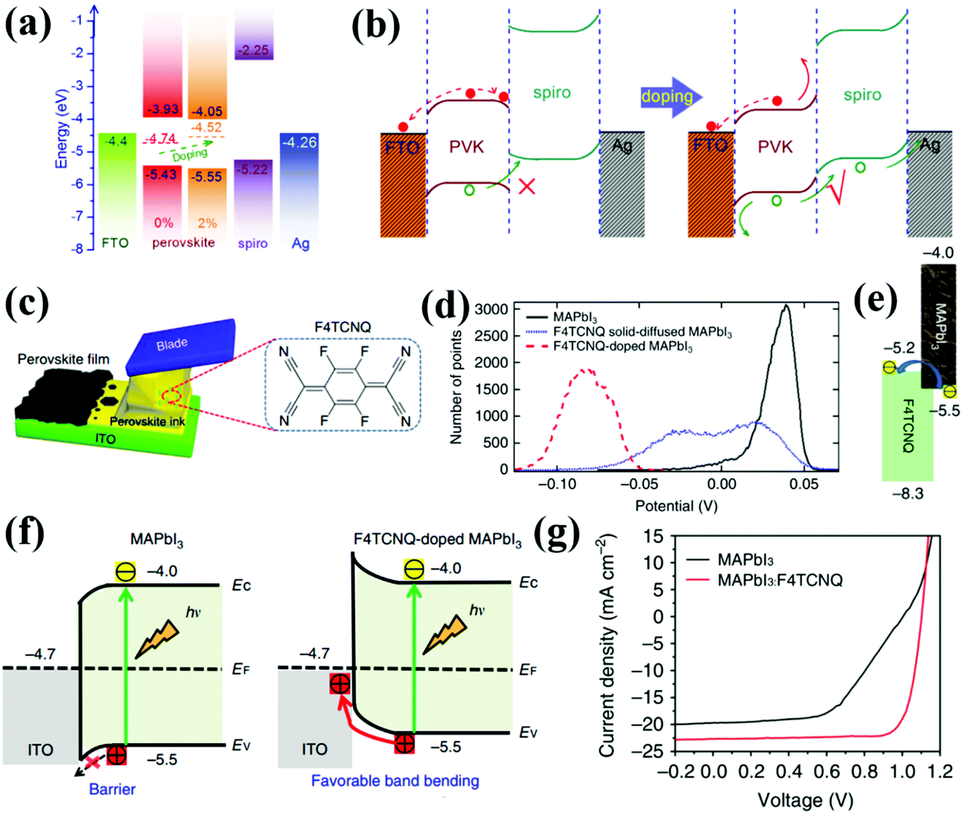 | ||
| Fig. 11 (a) Schematic energy level diagram of an ETL-free PSC with Sb doping. (b) Illustration of the interfacial charge transfer and band bending for ETL-free devices without or with Sb doping.77 Reproduced from ref. 77 with permission from John Wiley and Sons, copyright 2019. (c) Schematic of blade-coating of the F4TCNQ-doped perovskite film. (d) Surface potential profiles of MAPbI3, F4TCNQ-doped MAPbI3 and F4TCNQ solid-diffused MAPbI3 films. (e) Schematic illustration of the energy diagram and electron transfer process for MAPbI3:F4TCNQ blends. (f) Schematic illustration of hole transfer at the ITO/MAPbI3 or ITO/F4TCNQ-doped MAPbI3 interfaces. (g) J–V characteristics of HTL-free PSCs based on MAPbI3 and MAPbI3:F4TCNQ films.19 Reproduced from ref. 19 with permission from Springer Nature, copyright 2018. | ||
| Materials | Trap density (cm−3) | Mobility (cm2 V−1 s−1) | Diffusion length (μm) | Ref. |
|---|---|---|---|---|
| MAPbI3 | 1.4 × 10¹⁰ | 67.2 | 1.8–10 | 78 |
| MAPbBr3 | 3.0 × 10¹¹ | 24 | 1.3–4.3 | 78 |
| MAPbCl3 | 3.1 × 10¹⁰ | 42 | 3.0–8.5 | 79 |
| MAPbI3(Cl)x | 1.8 × 10⁹ | 167 | — | 80 |
| MAPbI3−xClx | — | — | 1.07 (electron) | 23 |
| — | — | 1.21 (hole) | 23 | |
| MA0.45FA0.55PbI3 | 2.6 × 10⁹ | 271 | 254 | 34 |
| CsPbBr3 | 1.1 × 10⁹ | 52 | 5.5 | 81 |
| FAPbBr3 | 9.6 × 10⁹ | 62 | 10.5 | 82 |
| FAPbI3 | 1.13 × 10¹⁰ | 35 | 1.7 | 82 |
Apart from composition engineering, the doping strategy has also been widely used in constructing efficient p–n heterojunctions to promote charge extraction in CTL-free PSCs. Doping can effectively tune the photoelectric properties (e.g., dopant levels, conductivity, carrier concentrations, Fermi levels and band bending directions) of semiconducting perovskite materials. Ge and co-workers have reported the n-type doping of MAPbI3 by Sb incorporation for ETL-free PSCs. Specifically, 2% Sb doping has shifted the Fermi level up from −4.74 eV to −4.52 eV, suggesting that the character of the perovskite changed from intrinsic to weak n-type (Fig. 11a). As mentioned above, electron injection from the intrinsic perovskite to FTO is energy favorable, whereas the hole extraction from the perovskite to the HTL is a limiting factor if there is no robust p–n junction. Without doping, downward band bending occurs at the perovskite/spiro-OMeTAD interface, which induces an energy barrier for hole extraction. After Sb-induced n-type doping, a Schottky-type p–n heterojunction is formed between the perovskite and spiro-OMeTAD, enabling upward interfacial band bending, which is beneficial for cascade hole extraction and electron blocking (Fig. 11b). As a result, an approximately 64% enhancement of PCE was achieved for the ETL-free PSC with Sb doping.77
The doping strategy has achieved exceptional success in HTL-free devices. In the case of p–i–n structured HTL-free PSCs with an inverted geometry, both electrons and holes can be transported to the ITO/perovskite interface and recombine there, leading to serious interfacial charge recombination and thus inferior charge collection. According to the energy level diagram (Fig. 12), downward band bending will occur at the ITO/perovskite interface, inducing an undesirable energy barrier for hole transfer from the perovskite to ITO. To tackle this obstacle, Huang and co-workers demonstrated the molecular doping of MAPbI3 with a strong electron-withdrawing molecule, 2,3,5,6-tetrafluoro-7,7,8,8-tetra-cyanoquinodimethane (F4TCNQ).19 F4TCNQ incorporation uniformly increases the work function of MAPbI3 to induce p-type doping (Fig. 11c and d). The doping mechanism can be explained by the fact that the deep lowest unoccupied molecular orbital (LUMO) level of F4TCNQ is close to the VBM of MAPbI3. The electrons in the VBM of MAPbI3 can be thermally activated into the LUMO level of F4TCNQ, which leaves holes in the MAPbI3 and thus causes it to be p-doped (Fig. 11e). Doping with F4TCNQ at 300 ppm significantly increased the carrier concentration up to 3 times, conductivity up to 10-fold, and induced upward band bending at the ITO/F4TCNQ-doped MAPbI3 interface, which then reduced the series resistance from 25.6 to 2.6 Ω cm2, and facilitated interfacial hole transfer and extraction from the perovskite to ITO (Fig. 11f). As a result, the PCE of the HTL-free PSCs doubled, showing an impressive PCE of 20.2% that completely outperformed pristine MAPbI3 (∼11%), along with high JSC, VOC and FF values of 22.7 mA cm−2, 1.10 V and 0.81, respectively (Fig. 11g).19 Further, this is the record efficiency for HTL-free PSCs, and the devices are made by the scalable blade-coating method. Similarly, Nakamura and co-workers doped MAPbI3 with a 0.03 wt% organic p-type semiconductor, fluorinated tetraarylbenzo[1,2-b:4,5-b′]dipyrrol-1,5-yl alkanediylsulfonate salt (BDPSO). The BDPSO-doped perovskite film enabled the fabrication of a HTL-free PSC with a PCE of 16.9%, which is 30% higher than that of a device without doping. BDPSO doping can not only efficiently facilitate charge separation and retard charge recombination, but also effectively passivate interfacial defects at the perovskite grain boundaries. In addition, HTL-free PSCs with BDPSO doping showed excellent operational stability with 93% of the initial PCE retained after continuous light soaking (1 sun with a 420 nm UV light cutoff filter) at the maximum power point for 1000 h. To take full advantage of the simplified device structure, a semitransparent HTL-free PSC was fabricated by reducing the thickness of the perovskite layer, striking a careful balance between the efficiency and transparency. PCEs of 10.3% and 8% were achieved when the device semitransparency was controlled at 22% and 30%, respectively.83
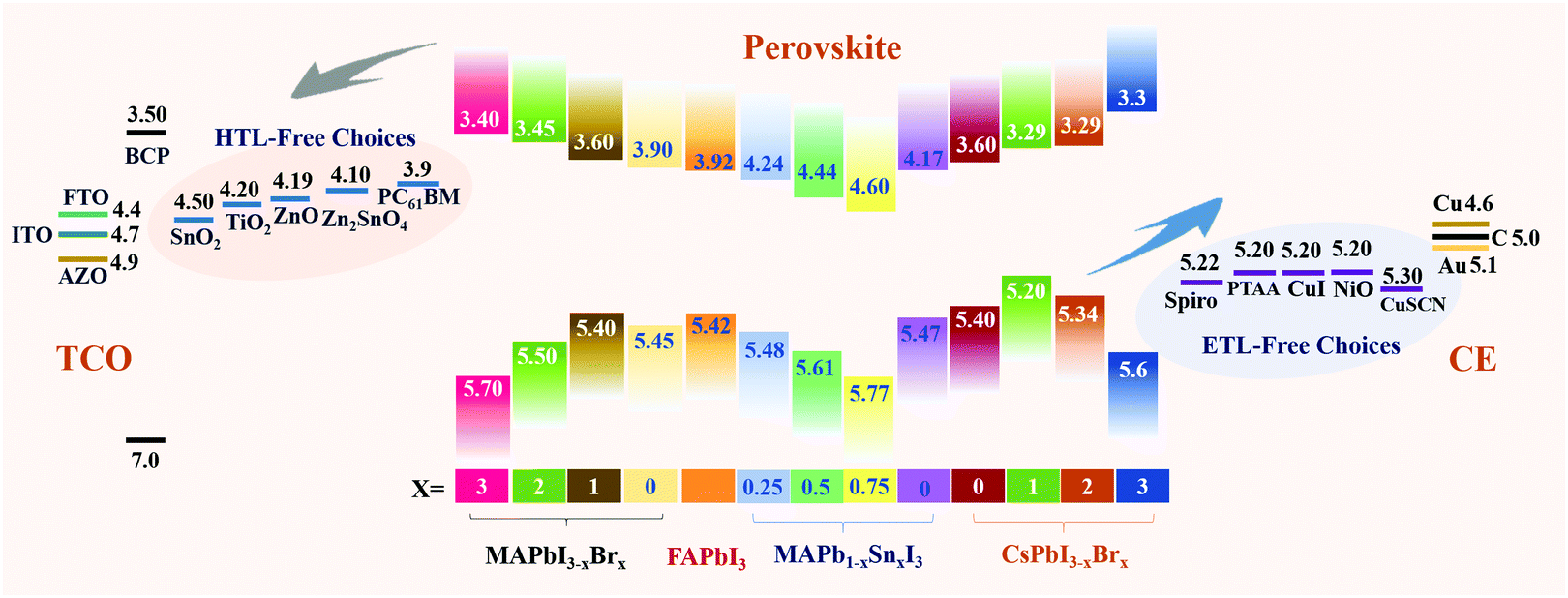 | ||
| Fig. 12 Schematic energy level diagram of perovskites of various compositions, TCO substrates, CTLs and CEs. | ||
In brief, the doping strategy prompts two rules for fabricating efficient CTL-free PSCs, namely, p-type doping of perovskites for HTL-free PSCs, and n-type doping of perovskites for ETL-free PSCs. However, the device performance is strongly related to the doping efficiency, which determines whether an effective p–n heterojunction has been formed. Superior to interfacial modification of the TCO substrate via additional material coating, the doping strategy really simplifies the fabrication procedure and device structure, simultaneously reducing the series resistance and boosting interfacial charge transfer within CTL-free PSC devices owing to the unique heterojunction merits. Choosing an appropriate dopant with suitable molecular or metal ion size is important. Owing to the ionic nature of the perovskite materials, doping with metal ions is more easily realized, with metal ions either replacing the B site cations in the perovskite or existing as heterogeneous impurities in the perovskite layer.84,85 In general, traditional doping of semiconductors will inevitably provoke charge recombination because the increased carrier concentration provides additional recombination centers. However, this phenomenon is not evident in doped perovskites because of the very good tolerance of defects by perovskite materials. On the other hand, it has been demonstrated that the trap sites within the organic–inorganic semiconductors can be reduced due to partial filling of crystal imperfections by doping, though typically at very low doping levels.
3.5 Device geometry engineering
Compared with polycrystalline perovskite thin films, bulk perovskite single crystals and thin-film perovskite single crystals are highly anticipated to achieve superior device performance in PSCs owing to their exceptional optoelectronic properties, such as high absorption coefficients and long charge-carrier diffusion lengths. With rapid development in preparing high-quality perovskite single cyrstals, the construction of lateral-structured devices has been achieved by directly growing perovskite single crystals on the grating electrode. A lateral PSC avoids the employment of an ETL and a HTL owing to the ultra-long charge diffusion length in the single crystal. Instead of collecting the charge carriers in a vertical direction (the carriers would need to travel across the crystal with a thickness of tens of micrometers), the carriers in the lateral PSC are collected laterally, and the charge transport pathway is shortened at least. Huang and co-workers designed a lateral-structured, single-crystal PSC with Au electrodes as both the cathode and anode (Fig. 13a), showing enhanced charge collection efficiency and yielding a PCE of 1.88% (Fig. 13b and c).86 The p and n regions were generated by ion migration through a piezoelectric poling process. However, the poling process would damage the crystals, thus deteriorating the device performance. To address this issue, the same group has demonstrated the use of a MAPbI3 single crystal wafer with thickness of only tens of micrometers. In addition, the ETL and hole blocking layer were introduced to facilitate the charge separation in the lateral device with a structure of Au/MAPbI3/C60/BCP/Au. As a result, a champion PCE of 5.9% has been attained for an HTL-free PSC with lateral geometry under 0.25 sun illumination.87 Bach and co-workers reported to grow a perovskite layer on two interdigitated, SAM-modified, gold back-contacts of opposite polarity (Fig. 13d). The SAM modification (4methoxythiophenol (OMeTP) and 4chlorothiophenol (ClTP)) resulted in the formation of a dipole field and Schottky junction at the respective metal/perovskite interfaces (Fig. 13e), which enabled selective charge extraction to the respective contacts. MAPbI3 films were deposited with four different cluster sizes denoted as large (L), mediate (M), small (S) and extra small (XS) (approximately 6.0, 2.0, 0.99, and 0.23 μm, respectively). Perovskite films with large cluster sizes exhibited longer charge recombination lifetimes, thus resulting in a higher VOC of 0.55 V. Simultaneously, charge injection from the large perovskite crystal to the electrode was also improved, which led to the highest PCE of 3.11% compared to the other devices (Fig. 13f).88 This work presented a new concept of constructing CTL-free PSCs, i.e. in the absence of both ETL and HTL. Specifically, the CTL-free PSC is composed of double Schottky junctions, which generate the built-in potentials for charge separation and extraction owing to the different work functions of the metal contacts modified by different functional molecules.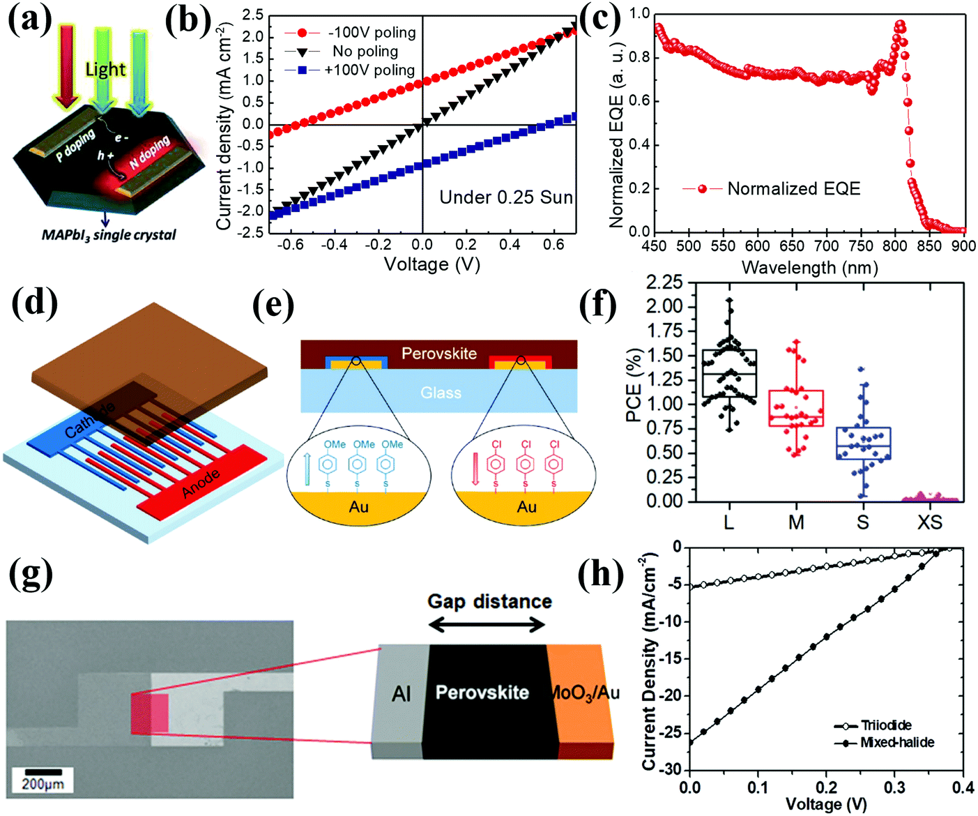 | ||
| Fig. 13 (a) Schematic device structure, (b) J–V curves measured under illumination of 0.25 sun and (c) charge collection efficiency of the lateral CTL-free PSC based on a MAPbI3 single-crystal.86 Reproduced from ref. 86 with permission from John Wiley and Sons, copyright 2016. (d) Schematic illustration of an interdigitated PSC. (e) Cross-section diagram of a dipole, SAM-modified, interdigitated, back-contact, CTL-free PSC with a device structure of Au/perovskite/Au. (f) PCE statistical distribution of back-contact PSCs based on perovskite films with large (L), media (M), small (S) and extra small (XS) cluster sizes (note: about 30 devices were measured for each condition).88 Reproduced from ref. 88 with permission from John Wiley and Sons, copyright 2018. (g) Optical microscopy image and the schematic of the lateral PSC with a structure of Al/MAPbI3−xClx/MoO3/Au. (h) J–V curves of lateral PSCs based on triiodide or mixed halide perovskites with a 500 nm gap under 1 sun illumination.89 Reproduced from ref. 89 with permission from John Wiley and Sons, copyright 2018. | ||
In the same way, this concept can also be realized by employing two different metals with different working functions, so that the asymmetric back-contacted device can be made. For example, Cho and co-workers demonstrated a lateral device with a structure of Al/MAPbI3−xClx/MoO3/Au. Different from the vertical PSC, the charges in the lateral PSC pass through multiple grain boundaries before being collected by the back-contacted metals (Fig. 13g). In this scenario, some portion of charge carriers will be consumed by the defects on the grain boundaries via trap-assisted recombination. However, the device performance is still limited by the inferior charge-carrier diffusion length in the polycrystalline perovskite film, which is relatively smaller than the spacing between the grating electrodes. It was found that the hole diffusion length in the mixed halide perovskite film (1.65 μm) was much longer than in a triiodide perovskite film (0.563 μm), despite similar electron diffusion lengths of 0.4–0.5 μm. As a result, the mixed halide perovskite-based lateral PSC achieved a PCE of 2.40%, which was three-fold higher than that of the triiodide perovskite-based counterpart (0.51%) (Fig. 13h).89
3.6 Carbon electrode for CTL-free PSCs
Though the construction of CTL-free PSCs can omit at least one preparation step and reduce by one third the fabrication cost, potential applications are still constrained by the utilization of highly priced metal CEs. For instance, one commonly used metal electrode, Au, is very expensive (about US$50 per gram), which is unrealistic and definitely limit the commercialization potential of CTL-free devices. We anticipate that future development trends of CTL-free PSCs will focus on employment of low-cost CE materials, such as copper or carbon, which have been predicted to improve the stability of PSCs up to 30 years or even life-long.90 Carbon is thought to be the most promising electrode candidate to achieve an optimal trade-off in the triangle of “efficiency–cost–stability”, which is advantageous for improving device efficiency and stability. To date, the most fashionable way to lower PSC production costs has been to forgo the expensive spiro-OMeTAD HTL, and replace the Au CE with a carbon electrode for the construction of HTL-free PSCs. Utilization of carbon electrodes in HTL-free PSCs is advantageous in three ways. First, the high work function of the carbon electrode (approximately −5.0 eV) enables the formation of a Schottky junction at the perovskite/carbon interface for efficient hole extraction. The built-in field at the perovskite/carbon interface facilitates the charge separation and contributes to achieving high VOC in carbon-based HTL-free PSCs. The type of interfacial junction observed is related to the work functions of the carbon electrode. The single-layered graphene (SG) has a lower working function than the multilayered graphene (MG), which forms an ohmic contact with the perovskite (Fig. 14a). In contrast, a Schottky junction was built at the interface between MG and perovskite, which was conducive to hole extraction and achieved a high PCE of 11.5% (Fig. 14b and c).91 This study highlighted the importance of tuning the work function and conductivity of the carbon electrode to improve the performance of HTL-free PSCs. The second advantage of using a carbon electrode is that the employment of a carbon electrode has significantly brought down the fabrication cost for PSCs, which makes viable the future commercialization of perovskite-based printed electronics. Yang and co-workers used C60 to replace TiO2 as the ETL, and a HTL-free all-carbon electrode-based PSC with a decent PCE of 15.38% has been achieved.92 Similarly, Guo and co-workers demonstrated the attractive and ideal concept of flexible HTL-free PSCs with both electrodes made of carbon: a graphene cathode and carbon nanotubes/carbon black anode.93 The third advantage of utilizing a carbon electrode in a HTL-free PSC is that the carbon electrode displays exceptionally good chemical inertness with the additional possibilities of self-encapsulation, water resistance, heat dissipation capability, all of which benefit the device stability. For instance, the demonstrated all-carbon electrode-based PSCs exhibit considerably enhanced stability when under thermal stress, retaining 89% of the initial PCE after 1570 h subjected to continuous treatment at 60 °C in the dark and in air. In sharp contrast, the PCEs for Ag- and Au-based control devices degraded to 26% and 52% of initial values, respectively.93 Though promising, the carbon electrode suffers from low conductivity and inferior contact with the perovskite layer. To tackle these drawbacks, one option to increase the electrode conductivity has been to incorporate the conductive carbon nanotubes or liquid metals (LMs) into the carbon electrode. Wang and co-workers incorporated single-walled carbon nanotubes into graphite/carbon black CEs. Benefiting from the improved conductivity, the carrier lifetime in the HTL-free devices was prolonged, leading to enhanced VOC and PCE.94 Liu and co-workers incorporated LM (Galinstan into the carbon electrode with different loading amounts of 0, 0.6, 1.2, and 2.0%). After LM incorporation, the interfacial charge transfer resistance decreased while charge recombination resistance increased (Fig. 14d), suggesting more efficient hole extraction and lower recombination rate at the perovskite/LM-incorporated carbon electrode interface. In particular, the incorporation of 1.2% LM resulted in an enhanced PCE of 13.51%, profiting from the greatly improved JSC and VOC (Fig. 14e). Additionally, the enhanced device performance can be ascribed to the high conductivity and superior fluidity of the LM, which improved the contact at the ZrO2/C interface and also facilitated hole extraction, thus reducing the possibility of carrier accumulation and recombination (Fig. 14f).95 Recently, Tang and co-workers reported a hypersimplified CTL-free PSC device with the stucture FTO/CsPbBr3/C, omitting both the ETL and HTL, suggesting great potential to further cut down the fabrication cost. Though only a sluggish PCE of 2.35% resulted, owing to severe recombination at the FTO/CsPbBr3 and CsPbBr3/C interfaces, this work paves the way for the development of next-generation CTL-free PSCs with a hypersimplified structure.96 We believe further enhancement in PCE can be achieved by combining optimization of composition, doping, p–n heterojunction and/or homojunction engineering, and improving the perovskite/C contact.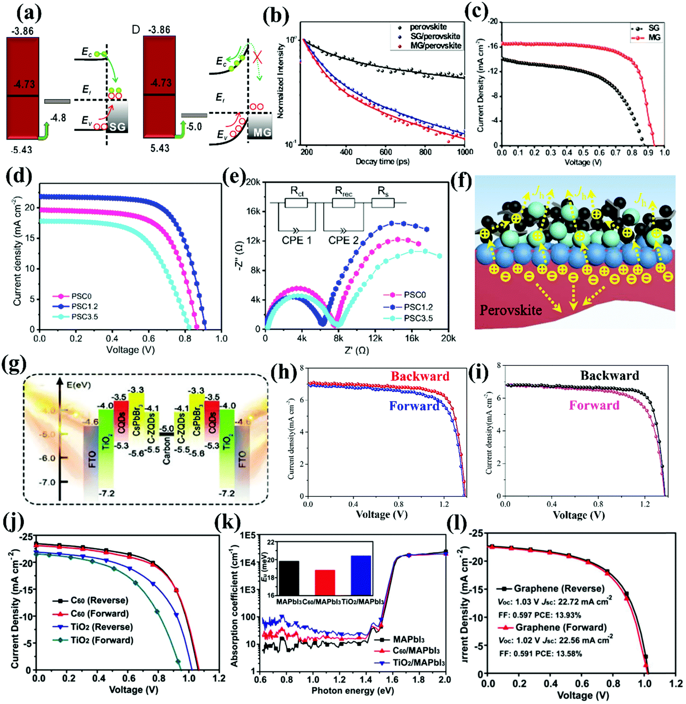 | ||
| Fig. 14 (a) Schematic diagram of ohmic contact at the SG/perovskite interface with possible recombination and Schottky junction at the MG/perovskite interface with directional hole transfer and electron blocking. (b) Hole extraction-induced TRPL decay of perovskite films in contact with SG or MG. (c) J–V curves of HTL-free PSCs based on a SG or MG electrode.91 Reproduced from ref. 91 with permission from John Wiley and Sons, copyright 2015. (d) J–V curves and (e) corresponding Nyquist plots of carbon-based HTL-free PSCs without (PSC0) LM, with LM contents of 1.2% (PSC1.2) and 3.5% (PSC3.5). (f) Schematic illustration of the hole extraction and transport at the perovskite/carbon interface with LMs.95 Reproduced from ref. 95 with permission from American Chemical Society, copyright 2018. (g) Energy band diagram of a bifacial PSC with a FTO/TiO2/CQDs/CsPbBr3/C-ZQDs/C/C-ZQDs/CsPbBr3/CQDs/TiO2/FTO configuration. J–V curves of CQDs/C-ZQDs modified, bifacial CTL-free PSCs measured in different scanning directions with irradiation from the (h) front and (i) rear.97 Reproduced from ref. 97 with permission from Royal Society of Chemistry, copyright 2018. (j) J–V curves of the PVSCs with C60 or TiO2 ETLs measured with the forward and reverse scans. (k) PDS absorbance spectra of MAPbI3 deposited on a C60 or TiO2 substrate (the inset compares the corresponding Urbach energies). (l) The stability of the PVSCs with C60 or TiO2 ETLs without encapsulation under ambient conditions with a relative humidity of 40–60% at room temperature.92 Reproduced from ref. 92 with permission from John Wiley and Sons, copyright 2018. | ||
Unlike the conventionally used thin layer of metal CEs, the carbon electrode normally needs to be thick enough (e.g. >25 μm) to ensure sufficient conductivity to collect charges. In carbon-based CTL-free PSCs, solar energy can only be harvested from the TCO glass side owing to the non-transparency of the carbon electrodes. Tang and co-workers developed the concept of a bifacial HTL-free PSC, which can absorb and convert incident light into electricity from both the front and rear sides. As illustrated in Fig. 14g, the device employs carbon quantum dots (CQDs) and ZnS quantum dots (C-ZQDs) in a mirrored configuration of FTO/TiO2/CQDs/CsPbBr3/C-ZQDs/C/C-ZQDs/CsPbBr3/CQDs/TiO2/FTO, where the front and rear cells share the same carbon electrode. The optimal PSC with this bifacial configuration yields a front efficiency of 7.55% and a rear efficiency of 7.44%, respectively, with a bifacial factor (BF) of up to 98.5% (Fig. 14h and i).97
Directly printing the carbon electrode on top of the perovskite layer is promising, but is still technically difficult to implement, since most of the commercially available carbon pastes and inks are not compatible with perovskites. To avoid undesirable damaging of the perovskite layer by carbon paste solvents, Meng and co-workers demonstrated the use of an as-prepared, free-standing carbon film which directly adheres to the surface of the PSC device with excellent interfacial contacts.98 In addition, a high-quality carbon electrode normally requires high temperature calcination to remove residual solvents and thus improve the conductivity. However, the underlying perovskite layer is vulnerable, to either high temperature or the polar organic solvents used with the carbon electrode. Zhou and co-workers have developed a low-temperature conductive carbon ink, which can be directly coated on top of the MAPbI3 film at 70 °C. The HTL-free PSC with a simplified structure of FTO/c-TiO2/m-TiO2/MAPbI3/C achieved a PCE of 9.08%.46
The most promising benefit of using a carbon electrode is to significantly reduce the fabrication cost, since the usage of the most expensive metal electrode has been avoided. It is worth mentioning that the carbon material can be fabricated as both the CE and front electrode. For instance, Yang and co-workers have fabricated a HTL-free PSC with a device structure of FTO/C60/MAPbI3/C. Surprisingly, a PCE of up to 15.38% was attained without J–V hysteresis, which is much higher than that of its TiO2 ETL-based counterpart (12.06%) (Fig. 14j). Photothermal deflection absorption spectroscopy (PDS) showed that C60 could reduce the number of trap states at the ETL/MAPbI3 interface (Fig. 14k), which is beneficial for suppressing the charge recombination and thus improving VOC. Further attempts to utilize graphene to replace the expensive TCO have been made to fabricate an all-carbon based HTL-free PSC, which yielded a decent PCE of 13.93% (Fig. 14l). The implementation of all-carbon based CTL-free PSCs has showcased the great potential for future commercialization on account of the favorable balance of cost, efficiency, and stability.92 Nevertheless, the PCEs of carbon electrode-based, CTL-free PSCs are still much lower than those of the conventional PSCs with CTLs and metal CEs, which could be ascribed to inferior contact, severe charge recombination at the perovskite/carbon interface, as well as insufficient sheet resistance of the carbon electrodes. Consequently, a deeper understanding of the charge transfer process at the perovskite/carbon interface is in high demand.
4. Conclusions and outlook
This review has highlighted recent advances in the development of strategies to assemble high-performance CTL-free PSCs with simplified device structures and reduced fabrication costs, including TCO/electrode modification, perovskite morphology optimization, heterojunction engineering, carrier dynamics tuning, device geometry engineering and employing low-cost carbon electrodes. The most plausible working mechanisms and a solid theory basis for CTL-free PSCs were elucidated. We also provided a fundamental understanding of the carrier dynamics, heterojunction merits and behind device physics associated with the leading CTL-free PSCs. The photovoltaic parameters for the different types of CTL-free PSCs including HTL-free, ETL-free, or both HTL- and ETL-free devices are summarized in Table 2.| Structure | PCE (%) | J SC (mA cm−2) | V OC (V) | FF | Ref. |
|---|---|---|---|---|---|
| HTL-free PSCs | |||||
| FTO/TiO2/MAPbI3/Au | 5.5 | 16.1 | 0.63 | 0.57 | 15 |
| FTO/TiO2/MAPbI3/Au | 8.04 | 18.8 | 0.71 | 0.60 | 99 |
| FTO/TiO2/MAPbI3/Au | 7.20 | 16.03 | 0.73 | 0.61 | 37 |
| FTO/TiO2/ZrO2/MAPbI3/C | 6.64 | 12.4 | 0.87 | 0.61 | 100 |
| ITO/ZnO/MAPbI3/Ag | 11.6 | 17.2 | 1.01 | 0.66 | 18 |
| FTO/TiO2/CsPbBr3/C | 6.7 | 7.4 | 1.24 | 0.73 | 101 |
| FTO/nanoporous TiO2 spheres/CsPbBr3/C | 14.3 | 22.5 | 0.99 | 0.64 | 45 |
| FTO/c-TiO2/TiO2 nanosheet/m-ZrO2/MAPbI3/C | 10.6 | 20.1 | 0.86 | 0.61 | 46 |
| FTO/TiO2/CsBr/CsPbBr3/C | 10.7 | 11.80 | 1.26 | 0.72 | 50 |
| FTO/c-TiO2/CsPbIBr2/C | 4.7 | 8.7 | 0.95 | 0.56 | 62 |
| FTO/c-TiO2/CsPbIBr2/C | 9.16 | 10.66 | 1.24 | 0.69 | 61 |
| FTO/c-TiO2/MAPbI3/CsPbBrxI3−x/Ag | 11.3 | 19.21 | 0.95 | 0.62 | 68 |
| ITO/c-TiO2/MAPbI3−xClx + (CuSCN)/Au | 18.1 | 22.8 | 1.04 | 0.76 | 66 |
| ITO/MAPbI3−xClx + Cu(Tu)I/C60/BCP/Ag | 20.0 | 22.3 | 1.12 | 0.80 | 67 |
| FTO/c-ZnO/MAPbI3/C | 8.73 | 19.98 | 0.81 | 0.54 | 102 |
| FTO/c-SnO2/(FAPbI3)0.97(MAPbBr3)0.03/C | 12.8 | 19.50 | 1.03 | 0.64 | 47 |
| FTO/c-TiO2/m-TiO2/m-Al2O3/MAPbI3/C/SWCNTs | 14.7 | 21.26 | 1.01 | 0.69 | 94 |
| FTO/c-TiO2/m-TiO2/MAPbI3–SWCNT/CWCNT-C | 15.7 | 22.36 | 0.97 | 0.72 | 103 |
| FTO/c-TiO2/MAPbI3/MG | 11.5 | 16.7 | 0.94 | 0.73 | 91 |
| FTO/c-TiO2/MAPbI3/SG | 6.7 | 14.2 | 0.87 | 0.54 | 91 |
| FTO/c-TiO2/m-TiO2/m-ZrO2/(5-AVA)xMA1−xPbI3/C + LM | 13.5 | 21.8 | 0.91 | 0.67 | 95 |
| FTO/c-TiO2/m-TiO2/MAPbI3/C | 9.08 | 21.0 | 0.80 | 0.54 | 104 |
| FTO/c-TiO2/m-TiO2/MAPbI3/C | 8.31 | 16.7 | 0.90 | 0.55 | 105 |
| FTO/c-TiO2/MAPbBr3/C | 8.7 | 7.83 | 1.46 | 0.78 | 106 |
| FTO/m-TiO2 + silane SAM/m-ZrO2/MAPbI3/C | 12.7 | 19.5 | 0.87 | 0.75 | 48 |
| FTO/m-TiO2/m-Al2O3/m-ZrO2/MAPbI3/C | 13.4 | 22.89 | 0.95 | 0.62 | 49 |
| FTO/m-TiO2/m-ZrO2/(5-AVA)xMA1−xPbI3/C | 12.8 | 22.8 | 0.85 | 0.66 | 17 |
| FTO/m-TiO2/m-ZrO2/MAPbI3−x(BF4)x/C | 13.2 | 18.15 | 0.95 | 0.76 | 75 |
| FTO/m-TiO2/m-Al2O3/MAPbI3(SrCl2)0.1/C | 15.9 | 20.18 | 1.05 | 0.75 | 107 |
| PEDOT (2 nm) modified-ITO/MAPbI3−xClx/C60/BCP/Ag | 19.3 | 22.7 | 1.05 | 0.80 | 45 |
| ITO/MAPbI3:F4TCNQ/C60/BCP/Cu | 20.2 | 22.7 | 1.10 | 0.81 | 19 |
| ETL-free PSCs | |||||
| FTO/MAPbI3/spiro-OMeTAD/Au | 14.1 | 19.76 | 1.06 | 0.67 | 40 |
| Etched-FTO/MAPbI3/spiro-OMeTAD/Au | 18.5 | 22.48 | 1.11 | 0.74 | 42 |
| FTO/MAPbI3/spiro-OMeTAD/Au | 18.2 | 21.45 | 1.12 | 0.75 | 56 |
| FTO/BCP/MAPbI3/spiro-OMeTAD/Au | 19.0 | 22.35 | 1.10 | 0.77 | 108 |
| ITO/ITO:Cs2CO3/MAPbI3/spiro-OMeTAD/Au | 15.1 | 19.9 | 1.07 | 0.71 | 43 |
| ITO/Cs0.05FA0.80MA0.15PbI2.55Br0.45/spiro-OMeTAD/Au | 19.5 | 23.61 | 1.06 | 0.77 | 71 |
| FTO/TMAH/MAPbI3/spiro-OMeTAD/Au | 20.1 | 23.22 | 1.17 | 0.73 | 44 |
| ITO/TAPC/MAPbI3/spiro-OMeTAD/Au | 19.4 | 22.07 | 1.12 | 0.78 | 21 |
| FTO/n-type MAPbI3/spiro-OMeTAD/Au | 15.6 | 23.21 | 1.03 | 0.61 | 70 |
| FTO/maze-like MAPbI3/spiro-OMeTAD/Au | 18.5 | 22.2 | 1.08 | 0.77 | 57 |
| FTO/FA0.83Cs0.17Pb(I0.6Br0.4)3/spiro-OMeTAD/Au | 13.3 | 18.54 | 1.04 | 0.71 | 20 |
| ITO/PEDOT:PSS/MAPbI3 + PCBM/Ca/Al | 12.1 | 16.0 | 0.96 | 0.79 | 64 |
| FTO/MAPbI3:C70/spiro-OMeTAD/Au | 13.6 | 16.1 | 1.044 | 0.71 | 109 |
| FTO/c-TiO2/m-TiO2/m-Al2O3/MAPb1−ySb2y/3I3−xClx/C | 12.6 | 18.24 | 1.01 | 0.68 | 77 |
| FTO/c-TiO2/m-TiO2/Sm3+–CsPbBr3/C | 10.1 | 7.48 | 1.59 | 0.85 | 60 |
| FTO/c-TiO2/m-TiO2/CsPbBr3/C | 9.72 | 8.12 | 1.45 | 0.82 | 110 |
| FTO/c-TiO2/MAPbI3:C60/Au | 11.7 | 15.4 | 1.03 | 0.73 | 111 |
| ITO/PTAA/MAPbI3/Ti/Au | 18.1 | 22.5 | 1.03 | 0.78 | 53 |
| FTO/MAPbI3/spiro-OMeTAD/Au | 10.0 | 17.03 | 0.9 | 0.65 | 39 |
| AZO/MAPbI3/spiro-OMeTAD/Au | 10.2 | 16.68 | 0.88 | 0.70 | 39 |
| ITO/MAPbI3/spiro-OMeTAD/Au | 10.0 | 18.92 | 0.84 | 0.63 | 39 |
| Both ETL- and HTL-free PSCs | |||||
| FTO/CsPbBr3/C | 2.35 | 4.64 | 1.05 | 0.48 | 96 |
| ITO/CsSnI3/Au/Ti | 0.88 | 4.80 | 0.42 | 0.22 | 112 |
| FTO/n-type MAPbI3/p-type MAPbI3/Au | 8.08 | 21.81 | 0.80 | 0.46 | 74 |
| Au/MAPbI3 single crystal/Au | 1.88 | 2.28 | 0.82 | 86 | |
| Al/MAPbI3−xClx/MoO3/Au | 2.40 | 26.24 | 0.38 | 0.24 | 89 |
| Al/MAPbI3/MoO3/Au | 0.51 | 5.32 | 0.40 | 0.24 | 89 |
| PEDOT (1.6 nm)-modified ITO/MAPbI3−xClx modified with islands-like C60 (1 nm)/BCP/Ag | 18.2 | 22.3 | 1.08 | 0.76 | 46 |
| Au/OMETP/MAPbI3/ClTP/Au | 3.11 | 11.93 | 0.55 | 0.48 | 88 |
| FTO/m-Al2O3/MAPbI3−xClx/Au | 7.1 | 18.6 | 0.80 | 0.47 | 113 |
| FTO/MAPbI3−xClx/Au | 3.2 | 7.11 | 0.77 | 0.53 | 113 |
Accordingly, several factors to achieve high-performance CTL-free PSCs are identified. (1) A uniform and dense perovskite film with large grains, fewer defects and high crystallinity is a prerequisite to avoid device shunting or current leakage, and retard the interfacial charge recombination. (2) A matched energy level alignment at the TCO/perovskite and/or perovskite/CE interface is required, which favors charge extraction and transport in a cascading manner. (3) In most CTL-free PSCs, the formation and presence of a perovskite–CTL bulk heterojunction, perovskite–perovskite interfacial graded heterojunction, perovskite–perovskite p–n homojunction or perovskite/CE Schottky junction is beneficial to the facilitation of charge separation and extraction, as well as suppressing charge recombination. (4) Prolonged carrier lifetime, extended carrier diffusion length and high carrier mobility together contribute to improving the charge collection efficiency in CTL-free PSCs, regardless of the charge generation and extraction rate at sub-optimal contact interfaces. (5) Enlarging the interfacial contact area between the perovskite and remaining CTL or changing the device geometry from the vertical to lateral direction may either facilitate charge separation or physically shorten the charge transfer pathway, both of which are promising for the fabrication of high-performance CTL-free PSCs.
This review gives indicative answers to controversies associated with some of the identified factors. For instance, the selection of the TCO substrates is not that critical, especially in ETL-free PSCs, since there is always a driving force to promote cascade charge transfer from the perovskite to TCO. Then there was the question that how to reduce interfacial recombination loss in the absence of a CTL. Surprisingly, the key was not to improve the charge extraction rate at the TCO/perovskite. Instead, several research studies proved that prolonging the carrier lifetime in the bulk perovskite film and/or facilitating an increase of the charge separation rate at the remaining CTL/perovskite heterojunction was more important. Another common controversy was which perovskite morphology was suitable to be used in CTL-free PSCs. There is also a competition between planar and bulk heterojunctions. With that in mind, a textured perovskite morphology, e.g. the maze-like perovskite, seems more promising to be used in CTL-free devices, because it has an enlarged interfacial contact with the remaining CTL materials, which strengthens the heterojunction merits of facilitated charge separation and extraction at the interface. It is addressed repeatedly that at least one robust junction should be formed for the successful implementation of high-performance CTL-free PSCs. Hence, we proposed some empirical models to guide the design of simplified device structures, for instance, PbI2-rich or n-doped perovskites for ETL-free PSCs, and MAI-rich or p-doped perovskites for HTL-free PSCs (Fig. 15a and b). The essence of these empirical models is to construct a p–n junction between an n-type perovskite/p-type HTL in an ETL-free PSC or between an n-type ETL and p-type perovskite in a HTL-free device, in order to facilitate charge separation and extraction at the respective interfaces.
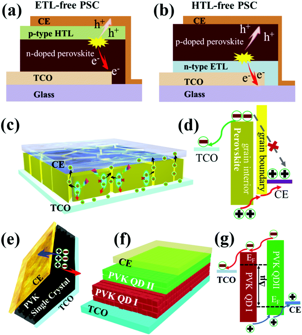 | ||
| Fig. 15 (a and b) Empirical models showing charge separation and the formation of n–p heterojunctions in (a) n-doped perovskites for ETL-free PSCs or (b) p-doped perovskites for HTL-free PSCs. (c and d) Schematic illustration of the proposed dopant-assisted charge dissociation at the interface between the grain interior and grain boundary owing to the difference in energy bands and conductivities. Both ETL and HTL-free PSCs based on (e) perovskite single crystals or (f) stacking of perovskite QDs with p–n homojunctions as well as (g) the cascade charge transport to the respective contacts via perovskite QD layers. | ||
In order to largely simplify the device structures, the ultimate goal is to construct CTL-free PSCs in the absence of both the ETL and the HTL. This is quite a challenge as two contacts/interfaces need to be optimized. We proposed several insightful strategies that can used to improve the performance of hyper-simplified CTL-free PSCs. First, through tuning the perovskite composition, doping or optimizing the film processing procedure, the dopant levels can convert the perovskite between p-type or n-type. Doping is the most direct way to achieve this. Specifically, a dopant of large molecular size prefers to stay at the grain boundaries of the perovskite, causing a huge discrepancy in conductivity between the grain interior and grain boundary (Fig. 15c). In this case, the dopant assists with charge dissociation at the interface between the grain interior and grain boundary. The highly conductive grain boundary is responsible for conducting one type of carrier depending on the doping levels of the perovskite (e.g. transporting holes in a p-doped perovskite), while another type of carrier will transport through the grain interior (Fig. 15d). This rational and effective charge separation and extraction model results in a more balanced transfer of electrons and holes to their respective electrodes, which decreases the possibility of charge accumulation and recombination. We anticipate that this charge separation and transport model can be used to guide the design and development of both ETL and HTL-free PSCs, since a rationally doped perovskite layer can itself perform light harvesting, charge separation and transport in a preferential manner. Third, perovskite single crystals possess superior charge carrier lifetime, stronger light absorption capability, and longer carrier diffusion length as compared to polycrystalline films. Therefore, it is reasonable to anticipate that perovskite single crystal thin films could be employed to fabricate high-performance both ETL and HTL-free PSCs as long as a favorable interface could be formed between the single crystalline perovskite and adjacent electrodes (Fig. 15e). The intentional stacking of two or multiple perovskite layers with gradient bandgaps that can form p–n homojunctions/heterojunctions and generate an electric field will be an efficient way to achieve charge separation and extraction in the perovskite film on its own without the assist of CTLs, which is promising to fabricate both HTL and ETL-free PSC. An optimal energy level alignment between multi-layered perovskites can be achieved, which enabled a cascade hole and electron extraction and conduction from the perovskite to the CE and TCO, respectively (Fig. 15f and g).
Considering the current status and challenges associated with the rapid developments in the field of CTL-free PSCs, we offer this insightful perspective on the future development and research directions of CTL-free PSCs, i.e. scalability, flexibility, non-toxicity and stability (Fig. 16). First, the currently reported CTL-free PSCs are all laboratory scale with a small area. Undoubtedly, fabrication of a large-area CTL-free PSC is highly desirable for the future practical application and commercialization. To achieve this, advanced scalable fabrication techniques need to be developed to print high-quality and uniform perovskite layers onto electrodes in a large-scale manner. Second, CTL-free PSCs can now be easily fabricated at low-temperatures. From a technical point of view, CTL-free PSCs can be implemented on flexible substrates, which is promising for flexible and light-weight printed electronics applications. Additionally, since flexible CTL-free PSCs have been rarely reported, this research direction is of great interest to the whole perovskite materials and devices community. Third, state-of-the-art CTL-free PSCs are all based on the lead-based perovskite materials, which has hindered their practical application in real life owing to the toxicity of Pb. Hence, it is meaningful to employ the low Pb or Pb-free perovskite compositions to construct CTL-free PSCs, which merits much more research interest and attention. Last but not least, there is still no absolute conclusion about the improved stability of CTL-free PSCs. Whether CTL-free PSCs have led to enhanced stability due to fewer interfaces or facilitated degradation due to heightened charge recombination? For this, the effect of internal and interfacial carrier dynamics on device stability should be further investigated.
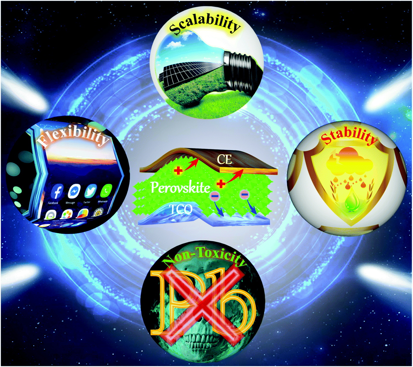 | ||
| Fig. 16 An insightful vision on the future development and research directions of CTL-free PSCs, namely, scalability, flexibility, non-toxicity and stability. | ||
Although the development of CTL-free PSCs is in its infancy, the prospects are almost undeniable. A more comprehensive understanding of the underlying working mechanism and photophysical processes, and advanced technological breakthroughs are highly desirable, which, when realized, will further improve the efficiency and stability of CTL-free perovskite photovoltaics, and pave the way for the commercialization of perovskite photovoltaic technologies. It is believed that the concept of simplified device structure will also provide useful guidance for achieving more efficient optoelectronic applications with simple operational systems, such as perovskite-based LEDs, photodetectors, phototransistors and photocatalysts.
Conflicts of interest
There are no conflicts to declare.Acknowledgements
This work was supported by Thousand Youth Talents Plan of China, Discovery program and DECRA fellowship (DE180101190) from Australian Research Council (ARC). D. B. Kuang acknowledges the financial support from the National Natural Science Foundation of China (21875288), the GDUPS (2016) and the Fundamental Research Funds for the Central Universities.Notes and references
- T. M. Brenner, D. A. Egger, L. Kronik, G. Hodes and D. Cahen, Nat. Rev. Mater., 2016, 1, 15007 CrossRef CAS.
- H. S. Rao, W. G. Li, B. X. Chen, D. B. Kuang and C. Y. Su, Adv. Mater., 2017, 29, 1602639 CrossRef PubMed.
- Y. Zhao, Q. Ye, Z. Chu, F. Gao, X. Zhang and J. You, Energy Environ. Mater., 2019, 2, 93–106 CrossRef CAS.
- Y. Liu, J. Cui, K. Du, H. Tian, Z. He, Q. Zhou, Z. Yang, Y. Deng, D. Chen and X. Zuo, Nat. Photonics, 2019, 13, 760–764 CrossRef CAS.
- https://www.nrel.gov/pv/assets/pdfs/champion-module-efficiencies.20190802.pdf .
- Z. Zhao, W. Sun, Y. Li, S. Ye, H. Rao, F. Gu, Z. Liu, Z. Bian and C. Huang, J. Mater. Chem. A, 2017, 5, 4756–4773 RSC.
- L. Huang and Z. Ge, Adv. Energy Mater., 2019, 9, 1900248 CrossRef.
- S. S. Shin, S. J. Lee and S. I. Seok, Adv. Funct. Mater., 2019, 1900455 CrossRef CAS.
- W.-Q. Wu, D. Chen, R. A. Caruso and Y.-B. Cheng, J. Mater. Chem. A, 2017, 5, 10092–10109 RSC.
- W. Q. Wu and L. Wang, Adv. Funct. Mater., 2018, 28, 1804356 CrossRef.
- Y. Li, S. Ye, W. Sun, W. Yan, Y. Li, Z. Bian, Z. Liu, S. Wang and C. Huang, J. Mater. Chem. A, 2015, 3, 18389–18394 RSC.
- J. A. Christians, P. Schulz, J. S. Tinkham, T. H. Schloemer, S. P. Harvey, B. J. Tremolet de Villers, A. Sellinger, J. J. Berry and J. M. Luther, Nat. Energy, 2018, 3, 68–74 CrossRef CAS.
- J. You, L. Meng, T.-B. Song, T.-F. Guo, Y. M. Yang, W.-H. Chang, Z. Hong, H. Chen, H. Zhou and Q. Chen, Nat. Nanotechnol., 2016, 11, 75–81 CrossRef CAS.
- T. Leijtens, G. E. Eperon, S. Pathak, A. Abate, M. M. Lee and H. J. Snaith, Nat. Commun., 2013, 4, 2885 CrossRef.
- L. Etgar, P. Gao, Z. Xue, Q. Peng, A. K. Chandiran, B. Liu, M. K. Nazeeruddin and M. Grätzel, J. Am. Chem. Soc., 2012, 134, 17396–17399 CrossRef CAS PubMed.
- Q. Wang, Y. Shao, H. Xie, L. Lyu, X. Liu, Y. Gao and J. Huang, Appl. Phys. Lett., 2014, 105, 163508 CrossRef.
- A. Mei, X. Li, L. Liu, Z. Ku, T. Liu, Y. Rong, M. Xu, M. Hu, J. Chen and Y. Yang, Science, 2014, 345, 295–298 CrossRef CAS.
- D. Liu, J. Yang and T. L. Kelly, J. Am. Chem. Soc., 2014, 136, 17116–17122 CrossRef CAS PubMed.
- W.-Q. Wu, Q. Wang, Y. Fang, Y. Shao, S. Tang, Y. Deng, H. Lu, Y. Liu, T. Li and Z. Yang, Nat. Commun., 2018, 9, 1625 CrossRef.
- Z. Hu, H. Xiang, M. S. Sebag, L. Billot, L. Aigouy and Z. Chen, Chem. Commun., 2018, 54, 2623–2626 RSC.
- W. Kong, W. Li, C. Liu, H. Liu, J. Miao, W. Wang, S. Chen, M. Hu, D. Li and A. Amini, ACS Nano, 2019, 13, 1625–1634 CrossRef CAS PubMed.
- C. Zuo, H. J. Bolink, H. Han, J. Huang, D. Cahen and L. Ding, Adv. Sci., 2016, 3, 1500324 CrossRef.
- S. D. Stranks, G. E. Eperon, G. Grancini, C. Menelaou, M. J. Alcocer, T. Leijtens, L. M. Herz, A. Petrozza and H. J. Snaith, Science, 2013, 342, 341–344 CrossRef CAS.
- M. M. Lee, J. Teuscher, T. Miyasaka, T. N. Murakami and H. J. Snaith, Science, 2012, 338, 643–647 CrossRef CAS.
- J. Shi, Y. Li, Y. Li, D. Li, Y. Luo, H. Wu and Q. Meng, Joule, 2018, 2, 1–23 CrossRef.
- Z. Guo, Y. Wan, M. Yang, J. Snaider, K. Zhu and L. Huang, Science, 2017, 356, 59–62 CrossRef CAS PubMed.
- J. Peng, Y. Chen, K. Zheng, T. Pullerits and Z. Liang, Chem. Soc. Rev., 2017, 46, 5714–5729 RSC.
- A. Marchioro, J. Teuscher, D. Friedrich, M. Kunst, R. Van De Krol, T. Moehl, M. Grätzel and J.-E. Moser, Nat. Photonics, 2014, 8, 250 CrossRef CAS.
- S. Aharon, I. Gdor, C. Yang, L. Etgar and S. Ruhman, J. Mater. Chem. A, 2016, 4, 3546–3553 RSC.
- C. S. Ponseca Jr, T. J. Savenije, M. Abdellah, K. Zheng, A. Yartsev, T. R. Pascher, T. Harlang, P. Chabera, T. Pullerits and A. Stepanov, J. Am. Chem. Soc., 2014, 136, 5189–5192 CrossRef PubMed.
- T. Ghosh, S. Aharon, L. Etgar and S. Ruhman, J. Am. Chem. Soc., 2017, 139, 18262–18270 CrossRef CAS PubMed.
- M. Hu, C. Bi, Y. Yuan, Z. Xiao, Q. Dong, Y. Shao and J. Huang, Small, 2015, 11, 2164–2169 CrossRef CAS PubMed.
- S. Collavini, S. F. Völker and J. L. Delgado, Angew. Chem., Int. Ed., 2015, 54, 9757–9759 CrossRef CAS PubMed.
- W.-G. Li, H.-S. Rao, B.-X. Chen, X.-D. Wang and D.-B. Kuang, J. Mater. Chem. A, 2017, 5, 19431–19438 RSC.
- D. Zheng, R. Peng, G. Wang, J. L. Logsdon, B. Wang, X. Hu, Y. Chen, V. P. Dravid, M. R. Wasielewski, J. Yu, W. Huang, Z. Ge, T. J. Marks and A. Facchetti, Adv. Mater., 2019, 31, 1903239 CrossRef CAS PubMed.
- J.-F. Liao, W.-Q. Wu, J.-X. Zhong, Y. Jiang, L. Wang and D.-B. Kuang, J. Mater. Chem. A, 2019, 7, 9025–9033 RSC.
- S. Aharon, S. Gamliel, B. El Cohen and L. Etgar, Phys. Chem. Chem. Phys., 2014, 16, 10512–10518 RSC.
- P. Wang, J. A. Dominguez-Caballero, D. J. Friedman and R. Menon, Prog. Photovoltaics, 2015, 23, 1073–1079 CAS.
- Q. Wei, Z. Yang, D. Yang, W. Zi, X. Ren, Y. Liu, X. Liu, J. Feng and S. F. Liu, Sol. Energy, 2016, 135, 654–661 CrossRef CAS.
- W. Ke, G. Fang, J. Wan, H. Tao, Q. Liu, L. Xiong, P. Qin, J. Wang, H. Lei and G. Yang, Nat. Commun., 2015, 6, 6700 CrossRef CAS PubMed.
- A. S. Chouhan, N. P. Jasti and S. Avasthi, Org. Electron., 2019, 66, 249–257 CrossRef CAS.
- H. Yu, J. W. Lee, J. Yun, K. Lee, J. Ryu, J. Lee, D. Hwang, S. K. Kim and J. Jang, Adv. Energy Mater., 2017, 7, 1700749 CrossRef.
- Q. Hu, J. Wu, C. Jiang, T. Liu, X. Que, R. Zhu and Q. Gong, ACS Nano, 2014, 8, 10161–10167 CrossRef CAS.
- C. Huang, P. Lin, N. Fu, C. Liu, B. Xu, K. Sun, D. Wang, X. Zeng and S. Ke, Chem. Commun., 2019, 55, 2777–2780 RSC.
- D. Liu, Q. Wang, M. Elinski, P. Chen, C. J. Traverse, C. Yang, M. Young, T. W. Hamann and R. R. Lunt, ACS Omega, 2018, 3, 6339–6345 CrossRef CAS PubMed.
- D. Liu, Q. Wang, C. J. Traverse, C. Yang, M. Young, P. S. Kuttipillai, S. Y. Lunt, T. W. Hamann and R. R. Lunt, ACS Nano, 2018, 12, 876–883 CrossRef CAS.
- Y. Xiao, C. Wang, K. K. Kondamareddy, N. Cheng, P. Liu, Y. Qiu, F. Qi, S. Kong, W. Liu and X.-Z. Zhao, ACS Appl. Energy Mater., 2018, 1, 5453–5462 CAS.
- Y. Rong, Z. Ku, A. Mei, T. Liu, M. Xu, S. Ko, X. Li and H. Han, J. Phys. Chem. Lett., 2014, 5, 2160–2164 CrossRef CAS PubMed.
- S. Lin, B. Yang, X. Qiu, J. Yan, J. Shi, Y. Yuan, W. Tan, X. Liu, H. Huang and Y. Gao, Org. Electron., 2018, 53, 235–241 CrossRef CAS.
- L. Liu, A. Mei, T. Liu, P. Jiang, Y. Sheng, L. Zhang and H. Han, J. Am. Chem. Soc., 2015, 137, 1790–1793 CrossRef CAS PubMed.
- Y. Xiong, X. Zhu, A. Mei, F. Qin, S. Liu, S. Zhang, Y. Jiang, Y. Zhou and H. Han, Sol. RRL, 2018, 2, 1800002 CrossRef.
- W. Zhu, Z. Zhang, W. Chai, Q. Zhang, D. Chen, Z. Lin, J. Chang, J. Zhang, C. Zhang and Y. Hao, ChemSusChem, 2019, 12, 2318–2325 CrossRef CAS PubMed.
- T. Chen, T. Shi, X. Li, J. Zheng, W. Fan, B. Ni, Y. Wang, J. Dai and Z. Xiao, Sol. RRL, 2018, 2, 1800167 CrossRef.
- W. Q. Wu, D. Chen, W. A. McMaster, Y. B. Cheng and R. A. Caruso, ACS Appl. Mater. Interfaces, 2017, 9, 31959–31967 CrossRef CAS PubMed.
- D. Bi, C. Yi, J. Luo, J.-D. Décoppet, F. Zhang, S. M. Zakeeruddin, X. Li, A. Hagfeldt and M. Grätzel, Nat. Energy, 2016, 1, 16142 CrossRef CAS.
- H. Yu, J. Ryu, J. W. Lee, J. Roh, K. Lee, J. Yun, J. Lee, Y. K. Kim, D. Hwang and J. Kang, ACS Appl. Mater. Interfaces, 2017, 9, 8113–8120 CrossRef CAS PubMed.
- J. F. Liao, W. Q. Wu, Y. Jiang, D. B. Kuang and L. Wang, Sol. RRL, 2019, 3, 1800268 CrossRef.
- J. F. Liao, H. S. Rao, B. X. Chen, D. B. Kuang and C. Y. Su, J. Mater. Chem. A, 2017, 5, 2066–2072 RSC.
- Z. Shao, Z. Wang, Z. Li, Y. Fan, H. Meng, R. Liu, Y. Wang, A. Hagfeldt, G. Cui and S. Pang, Angew. Chem., Int. Ed., 2019, 58, 5587–5591 CrossRef CAS PubMed.
- J. Duan, Y. Zhao, X. Yang, Y. Wang, B. He and Q. Tang, Adv. Energy Mater., 2018, 8, 1802346 CrossRef.
- W. Zhu, Q. Zhang, D. Chen, Z. Zhang, Z. Lin, J. Chang, J. Zhang, C. Zhang and Y. Hao, Adv. Energy Mater., 2018, 8, 1802080 CrossRef.
- Q. Ma, S. Huang, X. Wen, M. A. Green and A. W. Ho-Baillie, Adv. Energy Mater., 2016, 6, 1502202 CrossRef.
- W. Zhu, Z. Zhang, W. Chai, D. Chen, H. Xi, J. Chang, J. Zhang, C. Zhang and Y. Hao, ACS Appl. Energy Mater., 2019, 2, 5254–5262 CrossRef CAS.
- C.-H. Chiang and C.-G. Wu, Nat. Photonics, 2016, 10, 196 CrossRef CAS.
- C. Wu, K. Wang, Y. Yan, D. Yang, Y. Jiang, B. Chi, J. Liu, A. R. Esker, J. Rowe and A. J. Morris, Adv. Funct. Mater., 2019, 29, 1804419 CrossRef.
- S. Ye, H. Rao, W. Yan, Y. Li, W. Sun, H. Peng, Z. Liu, Z. Bian, Y. Li and C. Huang, Adv. Mater., 2016, 28, 9648–9654 CrossRef CAS PubMed.
- S. Ye, H. Rao, Z. Zhao, L. Zhang, H. Bao, W. Sun, Y. Li, F. Gu, J. Wang and Z. Liu, J. Am. Chem. Soc., 2017, 139, 7504–7512 CrossRef CAS PubMed.
- B. Li, Y. Zhang, L. Zhang and L. Yin, Adv. Mater., 2017, 29, 1701221 CrossRef PubMed.
- J. Liu, Q. Zhou, N. K. K. Thein, L. Tian, D. Jia, E. M. Johansson and X. Zhang, J. Mater. Chem. A, 2019, 7, 13777–13786 RSC.
- P. Cui, D. Wei, J. Ji, D. Song, Y. Li, X. Liu, J. Huang, T. Wang, J. You and M. Li, Sol. RRL, 2017, 1, 1600027 CrossRef.
- Q. Han, J. Ding, Y. Bai, T. Li, J.-Y. Ma, Y.-X. Chen, Y. Zhou, J. Liu, Q.-Q. Ge and J. Chen, Chem, 2018, 4, 2405–2417 CAS.
- M. Cai, N. Ishida, X. Li, X. Yang, T. Noda, Y. Wu, F. Xie, H. Naito, D. Fujita and L. Han, Joule, 2018, 2, 296–306 CrossRef CAS.
- Q. Zhao, A. Hazarika, X. Chen, S. P. Harvey, B. W. Larson, G. R. Teeter, J. Liu, T. Song, C. Xiao and L. Shaw, Nat. Commun., 2019, 10, 2842 CrossRef PubMed.
- P. Cui, D. Wei, J. Ji, H. Huang, E. Jia, S. Dou, T. Wang, W. Wang and M. Li, Nat. Energy, 2019, 4, 150–159 CrossRef CAS.
- J. Chen, Y. Rong, A. Mei, Y. Xiong, T. Liu, Y. Sheng, P. Jiang, L. Hong, Y. Guan and X. Zhu, Adv. Energy Mater., 2016, 6, 1502009 CrossRef.
- X. Xu, Q. Chen, Z. Hong, H. Zhou, Z. Liu, W.-H. Chang, P. Sun, H. Chen, N. D. Marco and M. Wang, Nano Lett., 2015, 15, 6514–6520 CrossRef CAS PubMed.
- L. Huang, S. Bu, D. Zhang, R. Peng, Q. Wei, Z. Ge and J. Zhang, Sol. RRL, 2019, 3, 1800274 CrossRef.
- M. I. Saidaminov, A. L. Abdelhady, B. Murali, E. Alarousu, V. M. Burlakov, W. Peng, I. Dursun, L. Wang, Y. He and G. Maculan, Nat. Commun., 2015, 6, 7586 CrossRef PubMed.
- G. Maculan, A. D. Sheikh, A. L. Abdelhady, M. I. Saidaminov, M. A. Haque, B. Murali, E. Alarousu, O. F. Mohammed, T. Wu and O. M. Bakr, J. Phys. Chem. Lett., 2015, 6, 3781–3786 CrossRef CAS PubMed.
- Z. Lian, Q. Yan, T. Gao, J. Ding, Q. Lv, C. Ning, Q. Li and J.-L. Sun, J. Am. Chem. Soc., 2016, 138, 9409–9412 CrossRef CAS PubMed.
- M. I. Saidaminov, M. A. Haque, J. Almutlaq, S. Sarmah, X. H. Miao, R. Begum, A. A. Zhumekenov, I. Dursun, N. Cho and B. Murali, Adv. Opt. Mater., 2017, 5, 1600704 CrossRef.
- A. A. Zhumekenov, M. I. Saidaminov, M. A. Haque, E. Alarousu, S. P. Sarmah, B. Murali, I. Dursun, X.-H. Miao, A. L. Abdelhady and T. Wu, ACS Energy Lett., 2016, 1, 32–37 CrossRef CAS.
- Z. Zhou, Z. Qiang, T. Sakamaki, I. Takei, R. Shang and E. Nakamura, ACS Appl. Mater. Interfaces, 2019, 11, 22603–22611 CrossRef CAS PubMed.
- P. N. Rudd and J. Huang, Trends Chem., 2019, 1, 394–409 CrossRef.
- H. W. Qiao, S. Yang, Y. Wang, X. Chen, T. Y. Wen, L. J. Tang, Q. Cheng, Y. Hou, H. Zhao and H. G. Yang, Adv. Mater., 2019, 31, 1804217 CrossRef.
- Q. Dong, J. Song, Y. Fang, Y. Shao, S. Ducharme and J. Huang, Adv. Mater., 2016, 28, 2816–2821 CrossRef CAS PubMed.
- Y. Liu, Q. Dong, Y. Fang, Y. Lin, Y. Deng and J. Huang, Adv. Funct. Mater., 2019, 1807707 CrossRef CAS.
- X. Lin, A. S. Chesman, S. R. Raga, A. D. Scully, L. Jiang, B. Tan, J. Lu, Y. B. Cheng and U. Bach, Adv. Funct. Mater., 2018, 28, 1805098 CrossRef.
- S. J. Yang, M. Kim, H. Ko, D. H. Sin, J. H. Sung, J. Mun, J. Rho, M. H. Jo and K. Cho, Adv. Funct. Mater., 2018, 28, 1804067 CrossRef.
- J. Zhao, X. Zheng, Y. Deng, T. Li, Y. Shao, A. Gruverman, J. Shield and J. Huang, Energy Environ. Sci., 2016, 9, 3650–3656 RSC.
- K. Yan, Z. Wei, J. Li, H. Chen, Y. Yi, X. Zheng, X. Long, Z. Wang, J. Wang and J. Xu, Small, 2015, 11, 2269–2274 CrossRef CAS.
- X. Meng, J. Zhou, J. Hou, X. Tao, S. H. Cheung, S. K. So and S. Yang, Adv. Mater., 2018, 30, 1706975 CrossRef PubMed.
- Q. Luo, H. Ma, Q. Hou, Y. Li, J. Ren, X. Dai, Z. Yao, Y. Zhou, L. Xiang and H. Du, Adv. Funct. Mater., 2018, 28, 1706777 CrossRef.
- H. Li, K. Cao, J. Cui, S. Liu, X. Qiao, Y. Shen and M. Wang, Nanoscale, 2016, 8, 6379–6385 RSC.
- Y. Zhang, J. Zhao, J. Zhang, X. Jiang, Z. Zhu and Q. Liu, ACS Appl. Mater. Interfaces, 2018, 10, 15616–15623 CrossRef CAS PubMed.
- J. Duan, Y. Zhao, B. He and Q. Tang, Small, 2018, 14, 1704443 CrossRef PubMed.
- Y. Li, J. Duan, Y. Zhao and Q. Tang, Chem. Commun., 2018, 54, 8237–8240 RSC.
- H. Zhang, J. Xiao, J. Shi, H. Su, Y. Luo, D. Li, H. Wu, Y. B. Cheng and Q. Meng, Adv. Funct. Mater., 2018, 28, 1802985 CrossRef.
- W. A. Laban and L. Etgar, Energy Environ. Sci., 2013, 6, 3249–3253 RSC.
- Z. Ku, Y. Rong, M. Xu, T. Liu and H. Han, Sci. Rep., 2013, 3, 3132 CrossRef PubMed.
- J. Liang, C. Wang, Y. Wang, Z. Xu, Z. Lu, Y. Ma, H. Zhu, Y. Hu, C. Xiao and X. Yi, J. Am. Chem. Soc., 2016, 138, 15829–15832 CrossRef CAS PubMed.
- H. Zhou, Y. Shi, K. Wang, Q. Dong, X. Bai, Y. Xing, Y. Du and T. Ma, J. Phys. Chem. C, 2015, 119, 4600–4605 CrossRef CAS.
- Y. Wang, H. Zhao, Y. Mei, H. Liu, S. Wang and X. Li, ACS Appl. Mater. Interfaces, 2018, 11, 916–923 CrossRef.
- H. Zhou, Y. Shi, Q. Dong, H. Zhang, Y. Xing, K. Wang, Y. Du and T. Ma, J. Phys. Chem. Lett., 2014, 5, 3241–3246 CrossRef CAS PubMed.
- F. Zhang, X. Yang, H. Wang, M. Cheng, J. Zhao and L. Sun, ACS Appl. Mater. Interfaces, 2014, 6, 16140–16146 CrossRef CAS PubMed.
- Y. Liang, Y. Wang, C. Mu, S. Wang, X. Wang, D. Xu and L. Sun, Adv. Energy Mater., 2018, 8, 1701159 CrossRef.
- H. Zhang, H. Wang, S. T. Williams, D. Xiong, W. Zhang, C. C. Chueh, W. Chen and A. K. Y. Jen, Adv. Mater., 2017, 29, 1606608 CrossRef PubMed.
- P. Zhao, M. Han, W. Yin, X. Zhao, S. G. Kim, Y. Yan, M. Kim, Y. J. Song, N. G. Park and H. S. Jung, ACS Appl. Mater. Interfaces, 2018, 10, 10132–10140 CrossRef CAS PubMed.
- J. Pascual, I. Kosta, E. Palacios-Lidon, A. Chuvilin, G. Grancini, M. K. Nazeeruddin, H. J. Grande, J. L. Delgado and R. N. Tena-Zaera, J. Phys. Chem. C, 2018, 122, 2512–2520 CrossRef CAS.
- J. Duan, Y. Zhao, B. He and Q. Tang, Angew. Chem., Int. Ed., 2018, 57, 3787–3791 CrossRef CAS PubMed.
- J. Pascual, I. Kosta, T. Tuyen Ngo, A. Chuvilin, G. Cabanero, H. J. Grande, E. M. Barea, I. Mora-Seró, J. L. Delgado and R. Tena-Zaera, ChemSusChem, 2016, 9, 2679–2685 CrossRef CAS PubMed.
- Z. Chen, J. J. Wang, Y. Ren, C. Yu and K. Shum, Appl. Phys. Lett., 2012, 101, 093901 CrossRef.
- Y. Zhang, M. Liu, G. E. Eperon, T. C. Leijtens, D. P. Mcmeekin, M. Saliba, W. Zhang, M. D. Bastiani, L. M. Herz, M. B. Johnston, H. Lin and H. J. Snaith, Mater. Horiz., 2015, 2, 315–322 RSC.
Footnote |
| † These authors contributed equally to this review. |
| This journal is © The Royal Society of Chemistry 2020 |