
Magnetic anisotropy of iridium dimers on two-dimensional materials
Miaomiao
Guo
a,
Xiaoqing
Liang
b,
Han
Wang
*c and
Junfeng
Zhang
 *ad
*ad
aSchool of Physics and Information Engineering, Shanxi Normal University, Linfen, 041004, China
bSchool of Electronics and Information Engineering, Taizhou University, Taizhou, 318000, China
cChemical Sciences Division, Lawrence Berkeley National Laboratory, Berkeley, California 94720, USA. E-mail: wangh@lbl.gov
dKey Laboratory of Spectral Measurement and Analysis of Shanxi Province, Shanxi Normal University, Linfen, 041004, China. E-mail: zhangjf@sxnu.edu.cn
First published on 22nd November 2019
Abstract
Magnetic dimers with very large magnetic anisotropy have great potential in information storage applications. By using density functional theory calculations (DFT), we systematically investigated the magnetic anisotropy energy (MAE) of bi-iridium (Ir2) dimers on four types of graphene-like two-dimensional (2D) material substrates. We considered four possible adsorption sites for Ir2 on each substrate. The Ir2 dimer prefers to remain at the single vacancy site with the largest binding energy for all the 2D materials considered. The spin moment and MAE of Ir2 can be largely affected by the substrate. On the substrate of germanene, the MAE of Ir2 can be enlarged to approximately 100 meV, even with the higher Ir2 areal density of 1.804 nm−2. Moreover, the direction of the easy magnetization axis is determined by the d states in the vicinity of the Fermi level. The present DFT results can be understood with the help of perturbation theory analysis.
1. Introduction
As one of the oldest branches of physics, magnetism has been utilized for both fundamental science and innovative spintronic devices.1 From low-dimensional nanostructures, clusters, and even down to single atoms,2,3 there has been great interest in nano-information storage devices because of their potential widespread applications. The low blocking temperature (BT),4 which denotes the threshold of temperature for maintaining thermal fluctuations of spin orientations, is one of the main stumbling blocks for development of information storage devices in practical applications. Scaled with BT, magnetic anisotropy energy (MAE), defined as the energy difference between the easy-axis and hard-axis, is a crucial parameter for magnetic stability. To maintain the spin orientation at room temperature at a long period, it is known that MAE should be at least 30 meV.5 Therefore, many efforts in past decades have been undertaken to search and tune candidates with larger MAE values.6–9Because of the strong spin–orbital coupling (SOC),10,11 it is expected that nanostructures containing 4d or 5d transition metal (TM) atoms will possess a possible larger MAE.12 There have been many attempts to increase the anisotropy barrier by disturbing the local ligand field.13,14 First, after assembling the magnetic atom into a single-molecule magnet with tens or hundreds of atoms,15 the MAE can be increased to 40 meV.6 Moreover, down to the TM dimer, the MAE can be remarkably enlarged,16–20 especially for Ni221 and Pt2 dimers,18 and because of the unique molecular orbital, a huge MAE (up to 220 meV per dimer) can be observed. Our recent work also suggested that by attaching a Br atom at one end of the Ir–Ir bond, a giant anisotropic magnet with MAE up to 294 meV can be obtained.7 However, a supporting substrate may be necessary for actual device realization. Related reports describe how magnetic atoms can be placed on substrates, e.g., single Co22 or single Co and Fe atoms on Pt(111),12 Pb(111),23 or MgO(001)24 substrates, and the MAE of 0.045 meV in bulk Co metal can be increased to 9 meV and 58 meV, respectively.
Since the discovery of graphene,25 there has been great interest in two-dimensional (2D) nanostructures because of their unique properties. Naturally, 2D materials can be utilized as supporting substrates. As a pioneering work, Xiao et al. studied Co–Co and Co–Ir dimers on benzene and graphene,26 and reported a very large MAE of the order of 200 meV per molecule. Hu et al. systematically investigated homo- and hetero-dimers on both perfect and defective 2D materials, such as graphene,5 h-BN,27 and 2D covalent organic frameworks.28 They found that on the double vacancy site of h-BN, Ir2 dimer presented a large MAE (approximately 126 meV) and high structural stability.27 Additionally, Cao et al. found an enhanced MAE of Os atoms on fluorine functionalized graphene29 and Ir atoms on g-C3N4,30 the latter of which can be tuned by applying an electric field. Moreover, Zhang et al. found that when the dimers of (Tm, Er, Sm)–Ir are adsorbed onto graphene oxide, the MAE exceeded 200 meV, and Os–(Fe, Ru, Rh) dimer adsorbed on graphene possessed a huge MAE, typically larger than 100 meV.31,32 Ge et al. used double-vacancy graphene as the substrate and decorated it with Ir atoms, and then manipulated the MAE with an external electric field.33
All the above works suggest that as the supporting substrate, 2D materials can tailor the MAE of TM atoms/dimers and then have great potential for realize their promise. Therefore, it is worthwhile to continue exploring more alternative 2D substrates. Except for graphene, other atomic 2D materials with flat or buckled honeycomb lattice have also been proposed and fabricated, such as silicene,34,35 germanene,35,36 stanene,37 and black phosphorus (BP).38 However, the interaction between TM dimers and these 2D materials is still elusive.
2. Methods
In this study, by using density functional theory calculations (DFT), we systematically investigated the interaction between TM Ir2 dimers and 2D materials, i.e., silicene, germanene, stanene, and BP, and compared these with the interaction that occurs with graphene substrate. Different adsorption sites and areal densities were considered, on both perfect and defective 2D materials. Ir2 exhibited a larger MAE on germanene than that on graphene, and this large MAE (109.4 meV) was maintained even on higher areal density. The physics mechanism can be understood with the assistance of density of states analysis. Our studies showed that germanene may be a good candidate for supporting Ir2 dimer in high-storage device applications.The structural, magnetic, and electronic properties of Ir2 dimer-adsorbed 2D materials were studied by first-principle calculations as implemented in Vienna Ab initio Simulation Package (VASP) code.39 The ion-electron interaction was treated with projector-augmented plane wave (PAW) potentials,40 and the exchange–correlation potential was described by generalized gradient approximation (GGA) with the Perdew–Burke–Ernzerhof (PBE) functional.41 Different supercells, i.e., (7 × 7) for graphene, (5 × 5) for silicene, (4 × 4) for stanene, (4 × 4) for germanene, and (5 × 4) for BP were selected to ensure that the periodic separation in the in-plane direction was larger than 15 Å. A vacuum space of 30 Å in the out-of-plane direction was used to avoid spurious interactions between periodic images. The energy cutoff for the plane-wave basis was set to 500 eV. The atomic structures were fully relaxed without any symmetric constrains, with the total energy and force convergence criteria of 10−4 eV and 0.01 eV Å−1, respectively. In magnetic and electronic investigations, the convergence criterion for total energy was set to 10−6 eV, taking into consideration the effect of SOC. The Brillouin zone of the supercells was sampled by Monkhorst–Pack k-point mesh with separation of 0.02 Å−1.
3. Results and discussion
Our investigation of the properties of the Ir2 dimer, as shown in Table 1, reveal that the calculated Ir–Ir bond length is 2.21 Å, which is similar to the value obtained from previous DFT calculations7,18,42 and experiments.43 Additionally, the spin moment of 3.427 μB is also consistent with previous theoretical results.7,18,42 For the Ir2 dimer, the MAE can be defined as the energy difference between the magnetic moment parallel (‖) and perpendicular (⊥) to the Ir–Ir bond when considering SOC: MAE = E(‖) − E(⊥). The MAE of the free Ir2 dimer is 40.71 meV, which is a value that is very similar to that of a previous calculation (40.6 meV).44 It is noteworthy that the MAE is sensitive to the selection of exchange–correlation potential, e.g., the MAE of the Ir2 dimer is 77 meV from local density approximation (LDA) calculations.8 Then, we investigated the Ir2 adsorbed on 2D materials, i.e., graphene, silicene, germanene, stanene, and black phosphorus. Using graphene as an example, in Fig. 1, we depicted four types of adsorption locations: (1) top (T) site, (2) hollow (H) site, (3) bridge (B) site, and (4) single vacancy (SV) defect site.| Adsorption site | 2D Material | d | h | M s | M s (Ir1) | M s (Ir2) | E b | MAE |
|---|---|---|---|---|---|---|---|---|
| Free Ir2 dimer | 2.210 | 3.427 | 1.713 | 1.713 | 40.71 | |||
| H | Graphene | 2.210 | 1.781 | 0.382 | 0.037 | 0.344 | 2.136 | 31.56 |
| Silicene | 2.257 | 1.247 | 2.791 | 0.623 | 1.980 | 5.231 | 21.25 | |
| Germanene | 2.240 | 1.187 | 2.451 | 0.626 | 1.692 | 4.686 | 94.85 | |
| BP | 2.253 | 1.427 | 0.061 | −0.054 | 0.175 | 4.670 | — | |
| T | Graphene | 2.206 | 2.125 | 3.277 | 1.265 | 1.836 | 1.216 | 97.93 |
| BP | 2.260 | 1.801 | 1.649 | 0.322 | 1.195 | 2.973 | 51.31 | |
| SV | Graphene | 2.318 | 1.060 | 1.495 | 0.118 | 1.425 | 8.810 | 18.45 |
| Germanene | 2.286 | 1.021 | 1.362 | 0.130 | 1.219 | 7.006 | 99.63 | |
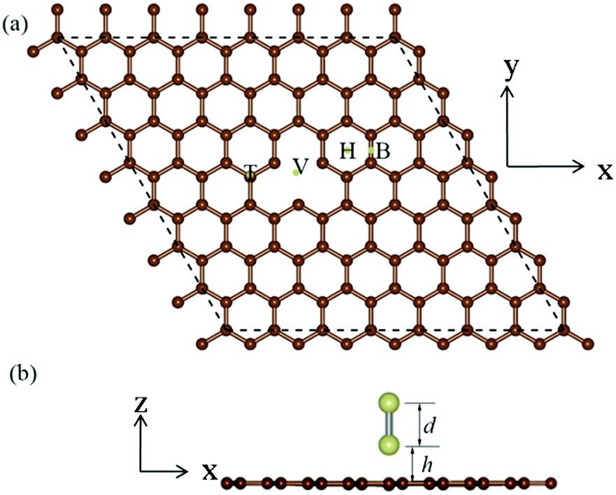 | ||
| Fig. 1 Schematic diagram of the geometry for Ir2 adsorbed on 2D material from the (a) top view and (b) side view. In (a), different adsorption sites are labeled as T (top site), H (hollow site), B (bridge site), and V (vacancy site), respectively. In (b), d represents the Ir–Ir bond length, and h is the distance between the bottom Ir atom and the 2D material. | ||
We considered the initial configurations with the Ir2 dimer perpendicular and parallel to the 2D sheets. The structural properties of Ir2-adsorbed 2D materials are listed in Table 1, where it has been noted that in some configurations, Ir–Ir bonds are not perpendicular but are parallel to or merged into the 2D sheets. These configurations (silicene: T and SV; germanene: T; BP: SV, and all configurations for stanene) are, therefore, not listed in Table 1. Compared with that for the Ir2 dimer, there is a less than 0.1 Å increase for most Ir–Ir bond lengths (d) of Ir2 when adsorbed on 2D materials, suggesting the negligible effect of the substrate. Additionally, the distance (h) from the bottom Ir atom (Ir1) to the substrate (see Fig. 1) ranged from 1.021 to 2.125 Å, depending on the detailed adsorption site. The structural stability can be measured by the binding energy defined as: Eb (in eV per Ir2) = EIr2 + E2D − EIr2–2D, where EIr2 is the total energy of isolated Ir2 dimer, E2D is the total energy of 2D material, and EIr2–2D is the total energy of the system with Ir2 adsorbed on a 2D material. The binding energy of Ir2 on the SV site of graphene (germanene) is 8.81 eV per Ir2 (7.006 eV per Ir2), which is much larger than that of the other sites, but slightly lower than that of the defective h-BN (9.13 eV per Ir2).27 This suggests that Ir2 can be quickly attracted to the single vacancy site on either the graphene or germanene substrate.
Table 1 shows that all considered systems are spin polarized, and the spin moments (Ms) are mainly localized on the Ir2. Compared with the free Ir2 dimer, Ms of Ir2 is lower and very sensitive to the substrate. Consistent with previous results of TM dimer on defective graphene,5 Ir1 has a smaller Ms (−0.054–1.265 μB), and the Ir atom far away the substrate (Ir2) is less affected by 2D material and has a larger Ms (0.175–1.980 μB). It is noteworthy that the in-plane easy-axis can be observed when Ir2 is adsorbed on the H site of BP, in which Ms will decrease to −0.054 μB for Ir1 and 0.175 μB for Ir2, respectively. When an Ir2 dimer is adsorbed on germanene, the system is unstable, and one Ir atom flies away from the T site. For both the H and SV sites of germanene, Ir1 has a smaller Ms than Ir2. In order to understand the magnetic moment of the Ir2 dimer as a function of the distance h, using Ir2 on the T site of graphene (ρgra = 0.451 nm−2) as an example, the magnetic moment for either Ir2 dimer or Ir atoms linearly changes with the increase in h. For Ir1 (near the substrate), the magnetic moment increases from 1.219 μB (h = 2.029 Å) to 1.543 μB (h = 2.429 Å), due to the weakened interaction between Ir1 and the C atom at the T site. Additionally, the magnetic moment of the other Ir atom decreases from 1.88 μB to 1.841 μB, and the magnetic moment for the Ir2 dimer slightly increases with the increase in h.
We next investigated the MAE of these configurations. By definition, the MAE is the energy difference between the magnetic moment parallel (‖) and perpendicular (⊥) to the atomic plane:
| MAE = E(‖) − E(⊥) | (1) |
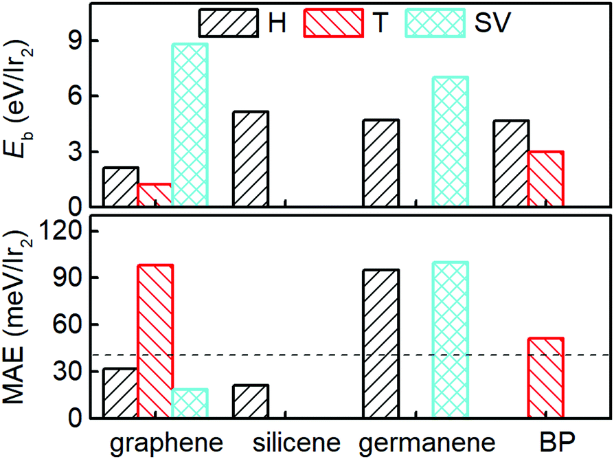 | ||
| Fig. 2 Binding energy (Eb) and MAE of the Ir2 dimer adsorbed on the H, T, and SV sites of different 2D materials. The dashed lines mark the MAE of the Ir2 dimer (40.71 meV) as a visual guide. | ||
We then studied germanene with different Ir2 densities (ρ), and compared them to the graphene case. The Ir2 density ranged from 0.389 to 4.77 nm−2 and from 0.451 to 1.804 nm−2 for graphene (ρgra) and germanene (ρger), respectively. With the increase in ρgra, the variation of d is less than 0.6% for all adsorption sites, but h can be enlarged by 4.6% for H and 11.7% for SV, respectively, with respect to that in the (7 × 7) graphene supercell (see Table 1). With the increase in ρger, the variation of d was less than 0.1%, which is consistent with that on graphene substrate. Being contrary with graphene, h for germanene slightly decreased (less than 0.75%) with the increase in ρger. We found that MAE is linearly functionalized with h, and only a 1.1% decrease in MAE occurred with a 6.7% increase in h. Therefore, we can safely neglect its effects. Because of the repulsive interaction of Ir2 from the periodic images, for the higher areal density, Ir2 can either fly away from the T site of graphene, or merge into the 2D sheet for the H or T site of germanene.
Fig. 3 shows Eb, Ms, and the MAE of Ir2 on graphene and germanene with different adsorption locations and different densities. The SV is always the most preferred site, with a larger Eb for both graphene and germanene. The Eb difference (approximately 2 eV) between the H and SV sites is quite small when Ir2 is absorbed on the germanene substrate, but it is quite large (approximately 7 eV) for Ir2 at different sites on the graphene substrate. A similar trend can be found for Ms, which is not sensitive to either ρgra or ρger, but is sensitive to the adsorption locations. The changes in MAE with different ρ values are shown in Fig. 3. For the most stable adsorption site (SV) of graphene, the MAE generally increases with the increase in ρgra, but most of the MAE values are smaller than that of free Ir2 dimer (40.71 meV). For the T site on graphene, the MAE is generally larger than 40 meV, but it is reduced with the increase in ρgra. We note that for ρgra = 4.77 nm−2, the MAE is abnormally large again, which probably results from the interactions between the periodic images of Ir2 in the (2 × 2) supercell. Furthermore, the Eb value is one of the most essential for Ir2 absorption. Therefore, low absorption energy (1.216 eV per Ir2 from Table 1) determines that Ir2 attached at the T site of graphene is not a practical device, even with a high MAE value. On germanene, for both the H and SV sites, the MAE generally increases with the increase in ρger, and the values are much larger than that on the graphene substrate or that of the free Ir2 dimer. All the above results suggest that because germane exhibits a larger Eb and MAE than graphene, germanene may be a more suitable substrate for use in information storage devices.
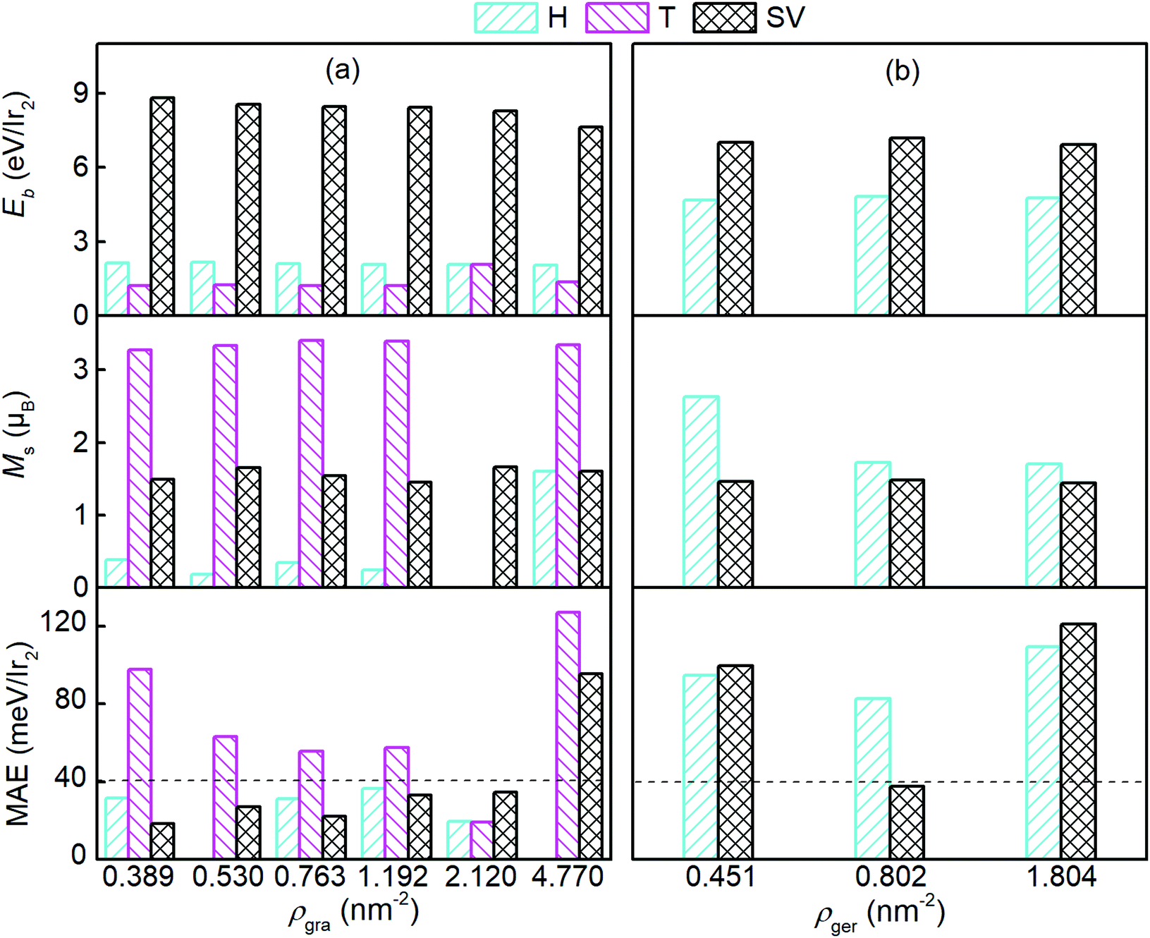 | ||
| Fig. 3 E b, Ms, and MAE of the Ir2 dimer on (a) graphene and (b) germanene with different densities. The dashed lines mark the MAE of the Ir2 dimer (40.71 meV). | ||
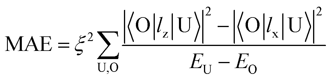
To understand the physical picture behind the varying MAE values of the Ir2 dimer, we discuss the difference between Ir2 on graphene and on germanene with the assistance of the second order perturbation approach proposed by Wang.10 Accordingly, MAE can be determined as:
 | (2) |
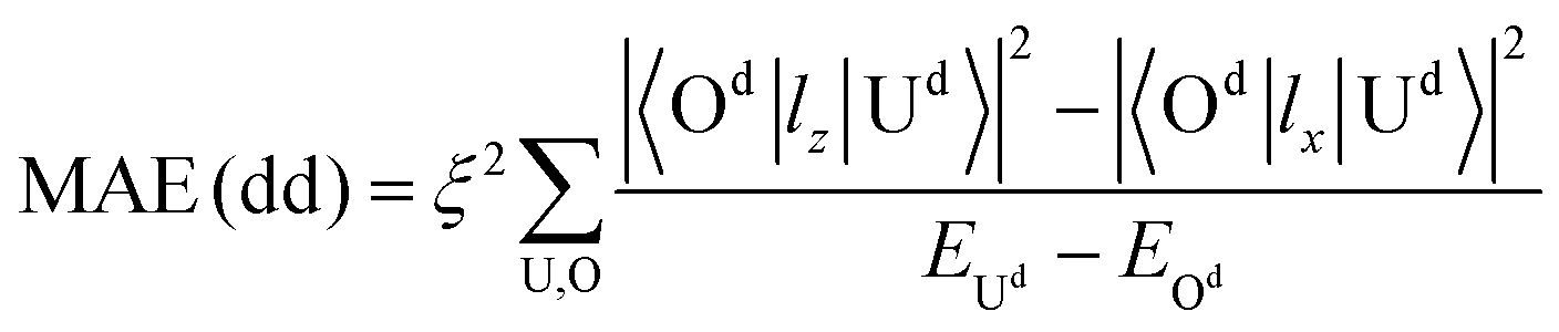 | (3) |
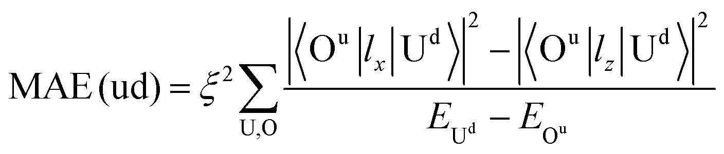 | (4) |
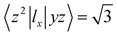 . Then, MAE can be obtained by analyzing the PDOS in a fixed energy range near the Fermi energy.
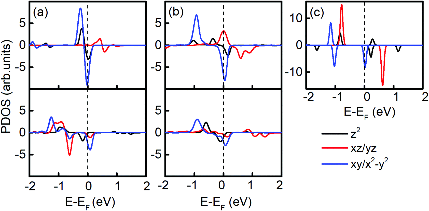 | ||
| Fig. 4 Projected density of states (PDOS) of (a) Ir2-graphene (upper: H site, lower: SV site), (b) Ir2-germanene (upper: H site, lower: SV site) and (c) free Ir2 dimer. The dashed lines label the Fermi level (EF). Black, red, and blue colors denote the contributions from the dz2, dxz/yz, and dxy/x2−y2 orbital, respectively. | ||
The PDOS in Fig. 4 shows the different contribution of d orbitals of free Ir2 dimer, and Ir2 on graphene (7 × 7) and germanene (4 × 4). Clearly, compared with the PDOS of Ir2 dimer, the band shifting in the Ir2-substrate system enables the MAE to be tunable. Three differences in the PDOS can be found between graphene- and germanene-supporting substrates. When adsorbed on the H site of graphene, the spin-up occupied state dxy/x2−y2 moved closer with EF, the spin-up occupied state dxz/yz changed to an unoccupied state, and the spin-down dz2 states moved down with the creation of two spin-up dz2 states. On the contrary, when Ir2 is adsorbed on the H site of germanene, the spin-up occupied state dxy/x2−y2 moved away from EF, and the spin-up occupied state dxy/x2−y2 and dxz/yz moved closer to EF. Additionally, the new created spin-up dz2 state is closer to EF than that of the Ir2 free dimer.
All these differences suggested that the smaller MAE can be assigned to graphene and the larger one assigned to germanene. A similar orbital shift can be found for SV configurations, as shown in the lower panel of Fig. 4(a) and (b). Considering the contributions from the dz2, dxz/yz, and dxy/x2−y2 orbitals, it is possible to calculate MAE using eqn (2). The MAE from eqn (2) (DFT calculations) in the energy range from −2 to 2 eV consists of free Ir2 dimer: 19.3ξ2 (40.71 meV), Ir2 on the H site of graphene: 15.2ξ2 (31.54 meV per Ir2), and Ir2 on the H site of germanene: 130.3ξ2 (94.84 meV per Ir2). Note that the MAE from eqn (2) depends on the selection of the energy range, which is due to the small fluctuation from the second order perturbation approach. However, the DFT results can generally be reproduced, and the different substrate effect on MAE is understandable.
As shown in Fig. 3(b), the MAE of Ir2 on the H or V site of germanene nonlinearly changes as the areal density increases from 0.451 nm−2 to 1.804 nm−2. To explore this phenomenon, in Fig. 5(a) and (b), we plotted the PDOS of Ir2 on the germanene H and SV sites, respectively. A nonlinear shift occurs for both dxy/x2−y2 and dxz/yz states with the increase in areal density. For example, in Fig. 5(a), the spin-up occupied state dxy/x2−y2 shifts away from the Fermi level with the areal density increase from 0.451 nm−2 to 0.802 nm−2. However, this state shifts closer to the Fermi level as the areal density increases from 0.802 nm−2 to 1.804 nm−2. As shown in Fig. 5(c) and (d), this type of nonlinear behavior can be reproduced from eqn (2), with the summarization within the energy range of (−2, 2 eV).
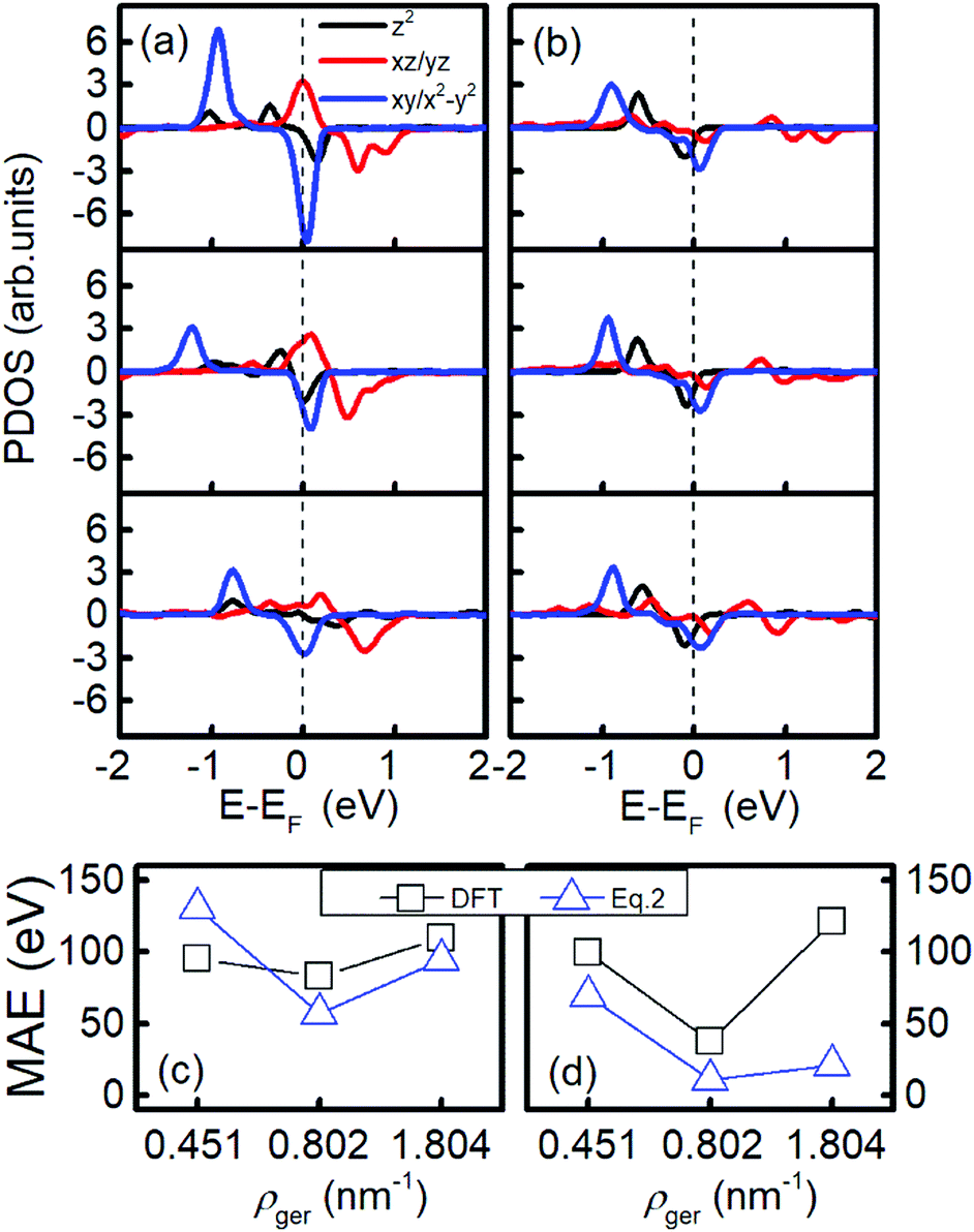 | ||
| Fig. 5 The PDOS and MAE of Ir2 adsorbed at the (a and c) H site and (b and d) SV site of germanene. In (a) and (b), the three parts from the top to bottom correspond to the Ir2 density of 0.451, 0.802, and 1.804 nm−2, respectively. The dashed line labels the Fermi level. In (c) and (d), the MAE from DFT and eqn (2) are labeled by black squares and blue triangles, respectively. | ||
4. Conclusions
In summary, the stability and magnetic properties of Ir2 dimers adsorbed on different 2D materials were investigated using first-principles calculations. When the Ir2 dimer remained at the single vacancy site, the binding energy was approximately two times larger compared with that of other adsorption sites. We also found that germanene is the ideal supporting substrate for the Ir2 dimer, because of its larger MAE of 121.01 meV. Moreover, the binding energy and MAE for Ir2 on germanene remain less affected with the higher areal density of 1.804 nm−2. The DFT results can be understood by the PDOS analysis with the assistance of the second order perturbation approach.Conflicts of interest
There are no conflicts to declare.Acknowledgements
This work is supported by the Scientific and Technological Innovation Programs of Higher Education Institutions in Shanxi (201802070) and the National Natural Science Foundation of China (11904251).References
- R. Wiesendanger, Rev. Mod. Phys., 2009, 81, 1495–1550 CrossRef CAS.
- T. Miyamachi, T. Schuh, T. Markl, C. Bresch, T. Balashov, A. Stohr, C. Karlewski, S. Andre, M. Marthaler, M. Hoffmann, M. Geilhufe, S. Ostanin, W. Hergert, I. Mertig, G. Schon, A. Ernst and W. Wulfhekel, Nature, 2013, 503, 242–246 CrossRef CAS PubMed.
- I. G. Rau, B. Susanne, R. Stefano, D. Fabio, S. Sebastian, G. Luca, D. Jan, P. Cinthia, N. Frithjof and G. Shruba, Science, 2014, 344, 988–992 CrossRef CAS PubMed.
- J. R. Friedman and M. P. Sarachik, Annu. Rev. Condens. Matter Phys., 2010, 1, 109–128 CrossRef CAS.
- J. Hu and R. Wu, Nano Lett., 2014, 14, 1853–1858 CrossRef CAS PubMed.
- P. Wang, X. Jiang, J. Hu, X. Huang and J. Zhao, J. Mater. Chem. C, 2016, 4, 2147–2154 RSC.
- X. Liang, X. Wu, J. Hu, J. Zhao and X. Zeng, Commun. Phys., 2018, 1, 74 CrossRef.
- J. Zhang, B. Yang, H. Zheng, X. Han and Y. Yan, Phys. Chem. Chem. Phys., 2017, 19, 24341–24347 RSC.
- Y. Wang, F. Li, H. Zheng, X. Han and Y. Yan, Phys. Chem. Chem. Phys., 2018, 20, 28162–28168 RSC.
- D. Wang, R. Wu and A. J. Freeman, Phys. Rev. B: Condens. Matter Mater. Phys., 1993, 47, 14932–14947 CrossRef CAS PubMed.
- R. Wu and A. J. Freeman, J. Magn. Magn. Mater., 1999, 200, 498–514 CrossRef CAS.
- P. Gambardella, S. Rusponi, M. Veronese, S. S. Dhesi, C. Grazioli, A. Dallmeyer, I. Cabria, R. Zeller, P. H. Dederichs, K. Kern, C. Carbone and H. Brune, Science, 2003, 300, 1130 CrossRef CAS PubMed.
- S. R. Chowdhury and S. Mishra, Phys. Chem. Chem. Phys., 2017, 19, 16914–16922 RSC.
- A. M. Pradipto, R. Broer and S. Picozzi, Phys. Chem. Chem. Phys., 2016, 18, 4078–4085 RSC.
- C. J. Milios, A. Vinslava, W. Wernsdorfer, S. Moggach, S. Parsons, S. P. Perlepes, G. Christou and E. K. Brechin, J. Am. Chem. Soc., 2007, 129, 2754 CrossRef CAS PubMed.
- P. Błoński and J. Hafner, J. Phys.: Condens. Matter, 2014, 26, 146002 CrossRef PubMed.
- F. Daniel, K. Klaus, R. Manuel and E. Helmut, J. Comput. Chem., 2008, 29, 2210 CrossRef PubMed.
- P. Błoński and J. Hafner, Phys. Rev. B: Condens. Matter Mater. Phys., 2009, 79, 224418 CrossRef.
- J. Mejía-López, A. Mejía-López and J. Mazo-Zuluaga, Phys. Chem. Chem. Phys., 2018, 20, 16528–16539 RSC.
- F. Cimpoesu, N. Dragoe, H. Ramanantoanina, W. Urland and C. Daul, Phys. Chem. Chem. Phys., 2014, 16, 11337–11348 RSC.
- Y. T. Chow, B. H. Jiang, C. H. Chang and J. S. Tsay, Phys. Chem. Chem. Phys., 2018, 20, 1504–1512 RSC.
- Y. Peng, T. Bodenstein, K. Fink, V. Mereacre, C. E. Anson and A. K. Powell, Phys. Chem. Chem. Phys., 2016, 18, 30135–30143 RSC.
- Y. Wang, X. Li, X. Zheng and J. Yang, Phys. Chem. Chem. Phys., 2018, 20, 26396–26404 RSC.
- S. B. Ileana, G. Rau, S. Rusponi and F. Donati, Science, 2014, 344, 988–992 CrossRef PubMed.
- K. S. Novoselov, A. K. Geim, S. V. Morozov, D. Jiang, Y. Zhang, S. V. Dubonos, I. V. Grigorieva and A. A. Firsov, Science, 2004, 306, 666–669 CrossRef CAS PubMed.
- R. Xiao, D. Fritsch, M. D. Kuz'min, K. Koepernik, H. Eschrig, M. Richter, K. Vietze and G. Seifert, Phys. Rev. Lett., 2009, 103, 187201 CrossRef PubMed.
- J. Li, H. Wang, J. Hu and R. Q. Wu, J. Chem. Phys., 2016, 144, 204704 CrossRef CAS PubMed.
- P. Wang, X. Jiang, J. Hu and J. Zhao, Adv. Sci., 2017, 4, 1700019 CrossRef PubMed.
- Y. Zhang, G. Zhu, J. Lu, Z. Guo and J. Cao, RSC Adv., 2015, 5, 87841–87846 RSC.
- Y. Zhang, Z. Wang and J. Cao, J. Mater. Chem. C, 2014, 2, 8817–8821 RSC.
- K. C. Zhang, Y. F. Li, Y. Liu, Y. Zhu and L. B. Shi, Phys. Chem. Chem. Phys., 2017, 19, 13245–13251 RSC.
- K. C. Zhang, Y. F. Li, Y. Liu and Y. Zhu, Phys. Chem. Chem. Phys., 2018, 20, 28169–28175 RSC.
- G. X. Ge, Y. B. Li, G. H. Wang and J. G. Wan, Phys. Chem. Chem. Phys., 2016, 18, 11550–11555 RSC.
- A. Kara, C. Léandri, M. E. Dávila, P. D. Padova, B. Ealet, H. Oughaddou, B. Aufray and G. L. Lay, J. Supercond. Novel Magn., 2009, 22, 259–263 CrossRef CAS.
- S. Cahangirov, M. Topsakal, E. Aktürk, H. Şahin and S. Ciraci, Phys. Rev. Lett., 2009, 102, 236804 CrossRef CAS PubMed.
- L. Li, S. Lu, J. Pan, Z. Qin, Y. Wang, Y. Wang, G. Cao, S. Du and H. Gao, Adv. Mater., 2014, 26, 4820–4824 CrossRef CAS PubMed.
- F. Zhu, W. Chen, Y. Xu, C. Gao, D. Guan, C. Liu, D. Qian, S. Zhang and J. Jia, Nat. Mater., 2015, 14, 1020–1025 CrossRef CAS PubMed.
- H. Liu, Y. Du, Y. Deng and P. D. Ye, Chem. Soc. Rev., 2015, 46, 2732–2743 RSC.
- G. Kresse and J. Furthmüller, Phys. Rev. B: Condens. Matter Mater. Phys., 1996, 54, 11169 CrossRef CAS PubMed.
- G. Kresse and D. Joubert, Phys. Rev. B: Condens. Matter Mater. Phys., 1999, 59, 1758–1775 CrossRef CAS.
- J. P. Perdew, K. Burke and M. Ernzerhof, Phys. Rev. Lett., 1996, 77, 3685 CrossRef PubMed.
- M. D. Morse, Chem. Rev., 1986, 86, 1049–1109 CrossRef CAS.
- Y. Han, G. Ge, J. Wan, J. Zhao, F. Song and G. Wang, Phys. Rev. B: Condens. Matter Mater. Phys., 2013, 87, 155408 CrossRef.
- X. Liang, X. Wu, X. Huang, Y. Su, J. Hu and J. Zhao, J. Cluster Sci., 2016, 27, 935–946 CrossRef CAS.
- H. Zheng, H. Han, J. Zheng and Y. Yan, Solid State Commun., 2018, 271, 66–70 CrossRef CAS.
| This journal is © the Owner Societies 2020 |