
Correlating hysteresis phenomena with interfacial charge accumulation in perovskite solar cells†
Tianyang
Chen
,
Zhe
Sun
 *,
Mao
Liang
and
Song
Xue
*
*,
Mao
Liang
and
Song
Xue
*
Tianjin Key Laboratory of Organic Solar Cells and Photochemical Conversion, School of Chemistry & Chemical Engineering, Tianjin University of Technology, Tianjin 300384, P. R. China. E-mail: zhesun@tjut.edu.cn; xuesong@ustc.edu.cn
First published on 28th November 2019
Abstract
The property of charge extraction at the contact between the perovskite and electron selective layer (ESL) is vital to the photovoltaic performance of perovskite solar cells (PSCs). The J–V hysteresis phenomenon is frequently observed when the PSC is limited by inefficient charge transfer across the perovskite/ESL interface. Drift–diffusion simulations are performed so as to correlate the hysteresis with the quality of the perovskite/ESL junction. A generalized charge exchange model is introduced into drift–diffusion equations for describing the dynamics of charge extraction at the perovskite/ESL contact. Our simulations demonstrate that inefficient charge extraction is one of the causes of j–V hysteresis. This is because limited charge transfer gives rise to a depletion domain in the ESL, and hence promotes the interfacial accumulation of charge carriers as well as movable ions. Furthermore, it is found that the incorporation of surface recombination into drift–diffusion simulations enables the loss in open circuit voltage to be simulated in PSCs with different charge transfer properties. The simulation results indicate that j–V hysteresis can be suppressed by improving the charge extraction property and suppressing surface recombination.
Introduction
Hybrid organic–inorganic perovskite solar cells (PSCs) have revolutionized the field of photovoltaics in recent years.1,2 In these devices, perovskite (PS) materials, as the kernel component, exhibit extraordinary optoelectronic properties, including high molar extinction coefficient, large diffusion length, and adjustable band gap. Due to these advantages, PSCs have become a promising candidate in replacing traditional silicon based photovoltaics. Up to now, the record power conversion efficiency (PCE) of PSCs has reached 25.2%.3,4 Apart from the notable achievement in cell efficiency, a variety of device configurations have been developed.2,5,6 Earlier PSCs were designed as a mesoporous structure, analogous to the configuration of solid dye sensitized solar cell.7 The huge area of the interface between the perovskite and mesoporous TiO2 plays an active role in promoting charge separation and hence improving device stability. Planar n–i–p or p–i–n configurations are also explored.8,9 With these configurations, the difficulty of low-temperature processing in PSC fabrication is largely reduced, which paves the way to realize roll-to-roll printing on a large-scale.10 In addition, perovskite/perovskite or perovskite(PS)/silicon(Si) tandem structures are employed for beating the single-junction Shockley–Queisser limit.11 Careful optimization of the interlayer contacts makes the open circuit voltage (Voc) approach 85–87% of the theoretical prediction.12Recently, more and more studies have unravelled the huge influence of the junction quality at both PS/electron selective layer (ESL) and hole selective layer (HSL)/PS contacts on the current–voltage (j–V) hysteresis and device performance.13–17 The hysteresis phenomenon in PSCs is of importance because it not only affects the correctness of PCE measurements but also reflects the physics of charge transport, ion redistribution, and the resultant variation of the electric field to some extent.18–21 Wojciechowski et al. demonstrated the reduction of j–V hysteresis by modifying the surface of a compact TiO2 layer with a monolayer of fullerene (C60) derivatives.22 Similarly, other electron acceptors, such as PCBM, n-type molecules and carbon quantum dots, are also valid in attenuating hysteresis because of their active role in promoting interfacial charge extraction.23,24 Moreover, j–V hysteresis can be suppressed alternatively by replacing the TiO2 based ESL with SnO2. It is interpreted as a result of the lower conduction band of SnO2 relative to the TiO2 counterpart by ∼250 meV.9 More driving force is therefore available for electron transfer across the SnO2/PS interface.9,25 However, the LUMO level of C60 derivatives is more negative than the conduction band edge of TiO2 by ∼200 meV.23 It excludes the explanation of interface band mismatching. Instead, the promoted charge transfer could be attributed to the strong donor–acceptor interaction between C60 derivatives and PS. In any event, these studies showed that the suppression of j–V hysteresis is linked to efficient interfacial charge transfer. However, the mechanism underlying such a relationship requires further investigation. One of the plausible interpretations of j–V hysteresis is the migration of movable ions, e.g. iodide and iodine vacancies, in the PS layer. The resultant accumulation of movable charges at the PS/ESL and/or PS/HSL interfaces gives rise to the screening of the internal electric field, and hence promotes or suppresses the extraction of charge carriers, i.e. electrons and holes. Indeed, the distribution of charge carriers and movable ions is connected to the internal electric field. When the charge extraction property is modified, the distribution of charge carriers at the charge selective interface is expected to change, which thereby leads to the variation of the internal electric field and engenders the redistribution of movable ions. Resultantly, different j–V characteristics would be observed. Although the variation of the electric field has been recorded using Kelvin probe force microscopy (KPFM), more information on charge accumulation at the contacts needs to be obtained.15
Device simulation based on drift–diffusion (D–D) equations provides a powerful tool in elucidating the charge transfer dynamics, recombination pathway, and ion migration in PSCs.26–29 Using numerical simulations, the validity of ion redistribution in interpreting hysteresis phenomena has been demonstrated.30–33 Bias preconditioning and/or varying scan-speed are shown to influence the profile of movable ions at the HSL/PS and PS/ESL interfaces significantly.27,31 Courtier et al. recently showed that the degree of hysteresis is dependent of the properties of the charge selective layer, such as permittivity and doping density.34 D–D simulations in combination with photovoltage/photocurrent transient measurements reveal that the degree of hysteresis is also relative to the rate of recombinaiton.30,35,36 Neukom et al. demonstrated that evident j–V hysteresis is observed when a PSC suffers from severe recombination, including bimolecular and/or trap-mediated recombination.32 It implies that high efficiency and less apparent hysteresis can be achieved simultaneously although ion migration still happens.
In this work, we aim to address how the property of charge extraction, i.e. junction quality, affects the distribution of charge carriers and moveable ions at the contacts, and hence changes the hysteresis behaviour. D–D simulations are therefore carried out. Different to previous simulations, the dynamics of interfacial charge transfer is described by a generalized charge exchange model. In this model, the difference in the Fermi-level at the PS/ESL interface is considered, by which j–V responses affected by the charge extraction dynamics are simulated. We show the emergence of j–V hysteresis by reducing the charge exchange rate even though recombination is significantly suppressed. The hysteresis behaviour is subsequently interpreted according to the profiles of charge carriers and accumulated ions. Furthermore, we discuss the effect of the charge extraction rate on the j–V hysteresis in the presence of surface recombination.
Model
A PSC with a planar HSL/PS/ESL configuration (shown in Fig. 1) is employed for simulating the dynamics of charge extraction and hysteresis behaviour. The simulations are implemented by solving the drift–diffusion (D–D) equations in one dimension. Movable cations and anions in the PS phase are allowed to redistribute in response to the electric field. The profile of movable ions is obtained by numerical implementation rather than pre-setting fixed ion accumulation layers or performing asymptotic treatments for simplifying the calculations at the HSL/PS and PS/ESL contacts.30 We assume that the charge loss in the PSC originates from both radiative recombination in the bulk of the PS layer and surface recombination at the contacts.26 The former is modelled as bimolecular reactions, whilst the latter is described by the Shockley–Read–Hall (SRH) equation.37 Note that surface recombination is assumed to occur at both the PS/ESL and HSL/PS boundaries. According to Courtier's scheme, the rate of surface recombination is limited by the densities of holes and electrons at the PS interface adjacent to the ESL and HSL layers, respectively.34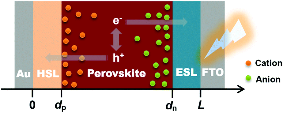 | ||
| Fig. 1 Device configuration of the perovskite model cell. The position of the boundaries is indicated. | ||
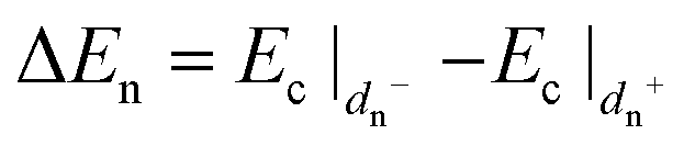
In our model, we consider PSCs with different charge transfer dynamics at the PS/ESL interface. Forward electron transfer from the PS to the ESL is driven by the difference in the Fermi-level at the boundary between the PS and the ESL. The driving force (ηn) is subsequently given by
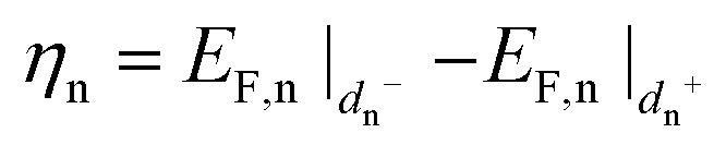 | (1) |
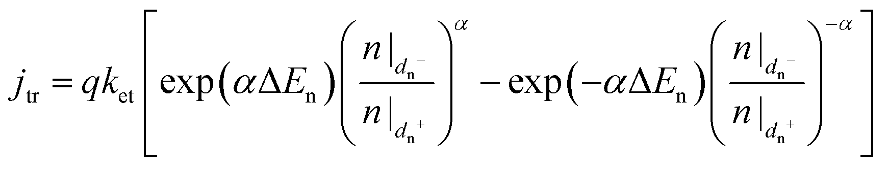
| jtr = qket[exp(−αηn) − exp(αηn)] | (2) |
 | (3) |
 | (4) |
 | (5) |
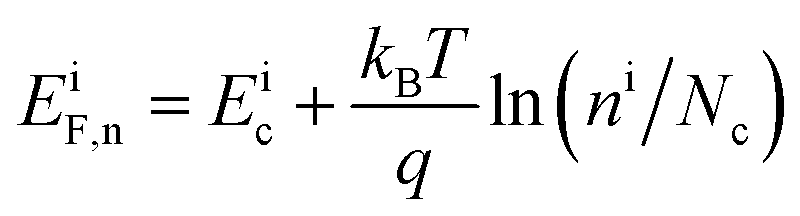
In the situation that exchange rate constant ket is large enough so that charge transport in the PSC is free from the limitation of interfacial electron transfer, a pseudo-equilibrium of charge carriers will be built at the PS/ESL interface.38 It means that  approximately equals
  . According to eqn (4), the electron densities at the PS side and the ESL side of the boundary satisfy,
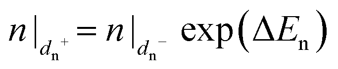 | (6) |
The charge transfer equation (eqn (4)) is incorporated into the D–D equations. These equations along with the numerical scheme are summarized in the ESI.† Briefly, the D–D equations are solved numerically by combining a finite-difference scheme with the relaxed iterative algorithm. Numerical solution of the D–D equations is difficult because of the problem of spatial stiffness, namely the density of charge carriers varies by several orders of magnitude in the narrower Debye layers (∼10 nm) at the PS/ESL and HSL/PS contacts. This difficulty can be overcome by using non-uniform grid spacing in combination with a finite element scheme.40 Alternatively, double-grid meshing associated with the Scharfetter–Gummel scheme is employed herein.41 Fine meshing of 0.1 nm is implemented in the Debye layers at both the HSL/PS and PS/ESL interfaces. In the rest of the device, a coarse grid of 5 nm is applied. It is demonstrated that such a spacing is sufficient to ensure the accuracy of the calculation.
Results and discussion
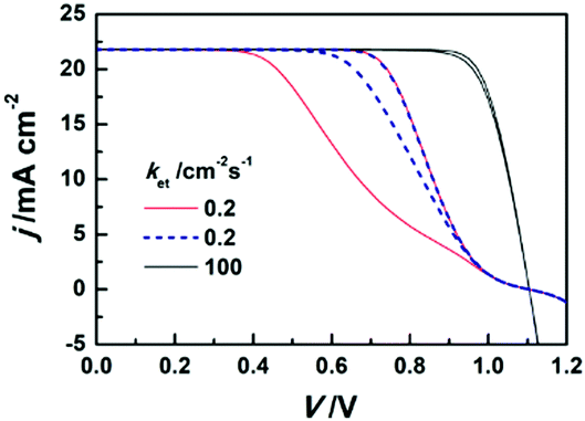
To address the effect of the charge transfer property on the photovoltaic responses of PSCs, we simulated the j–V curves in a mode of fast scanning.35 In this protocol, the PSC is preconditioned at a starting bias voltage until the charge carriers and mobile ions relax to their steady profiles. A fast j–V scan is then carried out, during which the ions are “fixed” at their initial position while the electrons and holes are allowed to drift under the variation of the bias voltage. The fixed ion distribution can be realized by setting the scan rate over 10 V s−1.18,32 It should be noted that the j–V scan in our simulations is not “ultra-fast”, namely it is slower than the redistribution of electrons and holes by 2–3 orders of magnitude. A quasi-equilibrium of charge carriers is expected to be established at each step of the voltage scan. For this reason, our simulations exclude transient behaviours of charge carriers on the time scale of microseconds.30 Previous studies have applied transient measurements in elucidating the dynamics of interfacial charge extraction and recombination.30,42 Incorporating the relaxation of charge carriers into j–V simulations, however, would give rise to a huge burden of computational cost.The effect of the charge extraction property on the j–V characteristics is displayed in Fig. 2. The j–V curves are simulated by performing a forward scan on the PSCs after preconditioning at short circuit, and then a reverse scan after annealing the PSCs at a bias voltage of 1.2 V. The dynamics of charge transfer is manipulated by tuning the rate constant of charge transfer at the PS/ESL boundary (ket). ket at the HSL/PS contact is fixed to 100 cm−2 s−1. This value is large enough so that no Fermi-level difference (ηn) arises according to our simulations. For simplicity, we firstly consider PSCs in which radiative recombination in the bulk of the PS is determinative. A series of j–V curves with ket from 100 to 0.2 cm−2 s−1 are plotted in Fig. 2a. The recombination rate constant (krb) for simulating these curves is fixed as low as 6 × 10⁻¹² cm3 s−1. It corresponds to the situation that bulk recombination in the PS layer is significantly suppressed. As expected, the j–V curves in the forward and reverse scans nearly coincide when ket is beyond 10 cm−2 s−1. In contrast, pronounced hysteresis is observed by reducing ket to 0.2 cm−2 s−1. Accordingly, the fill factor is 0.38 and 0.62 for the forward and reverse scans, respectively (see Fig. S3 in the ESI†). Neukom et al. have demonstrated that j–V hysteresis occurs in the case of rapid recombination in the bulk of the PS layer and/or at the contacts.32 In contrast, Fig. 2a indicates that a lower value of ket, corresponding to inefficient charge extraction, also results in j–V hysteresis. Not surprisingly, the decrease of ket engenders a substantial reduction of the power conversion efficiency (PCE) irrespective of the scan direction (Fig. S3 in the ESI†). It indicates the deterioration of the cell performance by limiting interfacial charge transfer. Similar conclusions can be drawn for PSCs suffering fast recombination. As indicated in Fig. 2b, a notable reduction of the short circuit current density in the forward scan is observed by setting ket to 0.2 cm−2 s−1. Moreover, Fig. 2a indicates that a ket below 1.0 cm−2 s−1 results in S-shape j–V curves. The S-shape curves emerge with a bias voltage close to the open circuit voltage (Voc). This is because less driving force can be provided for charge extraction. The photocurrent is resultantly limited by the rate of charge extraction. In other words, there is an imbalance between the generation of charge carriers and interfacial charge transfer.43
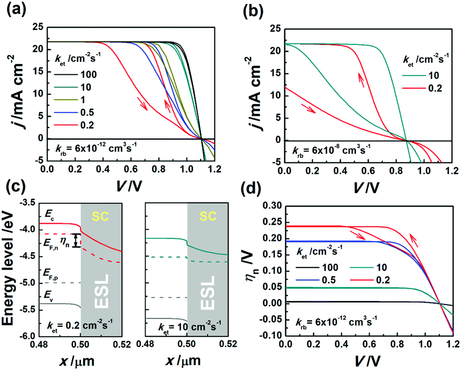 | ||
| Fig. 2 Dependence of j–V hysteresis on the charge transfer rate constant (ket). The radiative recombination rate constant (krb) is indicated in (a) and (b). The scan direction is indicated by arrows. (c) Energy diagram at the PS/ESL interface at short circuit (SC). The value of krb equals that in image (a). The driving force in charge transfer is indicated as ηn. (d) Variation of ηn with bias voltage under different ket shown in image (a). | ||
It is noted that Fig. 2 indicates that Voc is invariant with ket and the scan direction. This is due to the pre-setting in the simulation that the dominant charge loss in the PSCs is via bulk recombination. As mentioned above, the loss in Voc is replicated when surface recombination is introduced into the simulation. Indeed, Aygüler et al. have observed the invariance of Voc when the SnO2 based ESL shows different charge extraction behaviors.44 It implies that the limitation on charge extraction is not a direct cause of the Voc loss.
In Fig. 2c, we compare the energy diagram of the PS/ESL contact for ket equal to 10 and 0.2 cm−2 s−1. The whole picture of the energy diagram is displayed in Fig. S4 in the ESI.† As expected, charge transfer limitation (ket = 0.2 cm−2 s−1) engenders a Fermi-level difference of 240 mV (left panel). By contrast, an ηn of 50 mV is obtained for the PSC with less charge transfer resistance (right panel). Moreover, the variation of ηn with bias voltage is shown in Fig. 2d. It is seen that ηn rises evidently with the reduction of ket. It implies more driving force is required for charge transfer although the conduction band difference of 130 mV is invariant. When ket reaches 100 cm−2 s−1, the Fermi-level difference is close to zero. As previous studies have discussed, swift charge exchange makes the ratio of the electron density at the two sides of the contact (rPS/ESL) only depend on the conduction band difference.26,27,38 Interestingly, Fig. 2d shows that small ket results in the deviation of the forward ηn–V curve from the reverse counterpart. It seems that charge transfer limitation makes rPS/ESL more sensitive to the interfacial electric field, and hence engenders more apparent hysteresis.
We further display the density profiles of charge carriers and movable ions at short circuit in Fig. 3. It shows that the reduction of ket gives rise to higher electron density in the PS layer regardless of the scan direction. More importantly, electrons are found to accumulate at the left side of the PS/ESL contact when ket is reduced to 0.2 cm−2 s−1. At the right side of the contact, electrons are notably depleted. In comparison, neither charge accumulation nor depletion is observed when the PSC is free from charge transfer limitation (Fig. 3b and d). Moreover, it is seen that the variation of the charge transfer property has less impact on the profile of the hole density. A possible explanation is that the electric field is highly screened in the PS phase as displayed in Fig. 4a. The distribution of the hole density is mainly dominated by the diffusion coefficient rather than the profile of the electric field. Furthermore, the charge quantities of electrons and holes in the PS phase are calculated according to the simulation results. Fig. 5a shows that an evident increase of the electron quantity (−Qn) with the reduction of ket is observed in the forward scan, while the variation of the hole quantity (Qp) is less apparent. Here the sign of the charges is neglected for convenience. The accumulation of electrons and holes inside the PS layer is more apparent in the reverse scan, as shown in Fig. 5b. Such results are consistent with the j–V curves in Fig. 2a and b, which indicates an increase of the recombination rate due to charge transfer limitation irrespective of the scan direction.
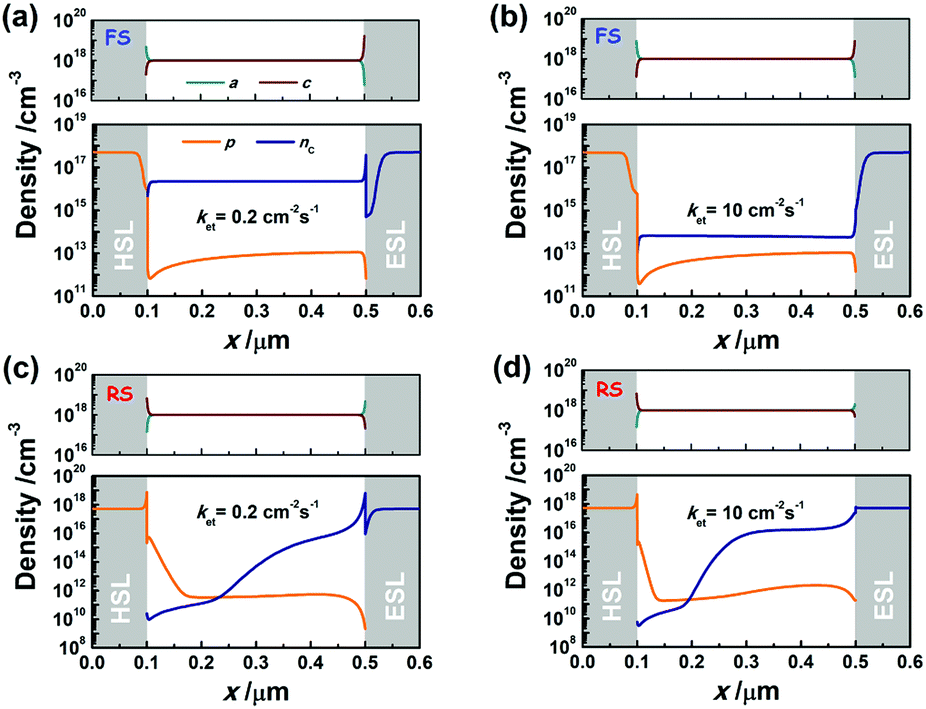 | ||
| Fig. 3 Density profiles of charge carriers and movable ions at short circuit. The profiles of movable ions are shown in the upper panels separately. Symbols “FS” and “RS” indicate forward and reverse scanning, respectively. Recombination rate constant krb is 6 × 10⁻¹² cm3 s−1. | ||
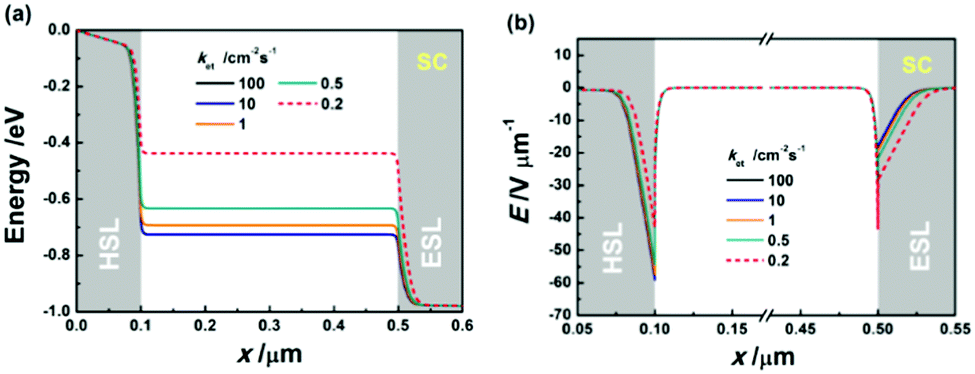 | ||
| Fig. 4 Profiles of electrostatic voltage (a) and electric field (b) at short circuit. Recombination rate constant krb is 6 × 10⁻¹² cm3 s−1. | ||
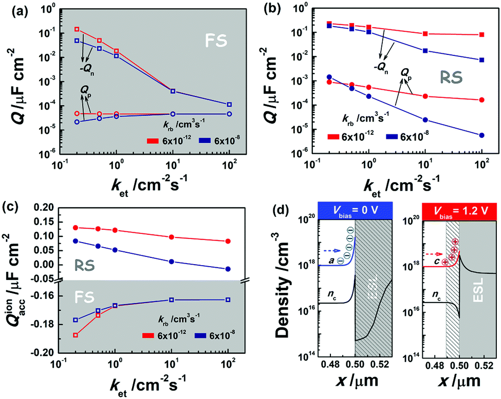 | ||
| Fig. 5 Plots of the charge quantities of electrons and holes in the perovskite layer against the charge transfer rate constant at short circuit with forward (a) and reverse (b) scanning. (c) Plots of the charge quantity of the accumulated ions at the PS/ESL contact as a function of the charge transfer rate constant. The curves in the gray and white regions are obtained from the forward and reverse scans, respectively. (d) Schematic of ion accumulation induced by charge transfer limitation (ket = 0.2 cm−2 s−1). The irradiated PSCs are annealed with a bias voltage of 0 (left panel) and 1.2 V (right panel). The shadow parts indicate the domains where electrons are depleted. | ||
It is further noticed that the limitation on charge transfer induces the accumulation of movable ions at the PS/ESL interface. To assess the extent of ion accumulation, we quantified the net charge of movable ions at the left side of the PS/ESL contact. According to the assumption, the average density of both movable cations and anions equals 1 × 1018 cm−3. It is convenient to calculate the accumulated charge (Qionacc) by simply integrating the distribution of ion density over the range from the middle of the PS phase to the PS/ESL boundary. Such a method is valid because the screening of the electric field engenders the compensation of positive and negative ion charges beyond the Debye layer. The plots of ion charge quantity as a function of the charge transfer rate constant are indicated in Fig. 5c. It shows that the reduction of the charge transfer rate constant gives rise to more evident accumulation of negative and positive charges for the forward and reverse scans, respectively. Accordingly, the electric field at the PS/ESL interface shown in Fig. 4b is enlarged, which plays a key role in suppressing charge extraction. To figure out the origin of the induced ion accumulation, we illustrate the density profiles of electrons and anions in the region of the PS/ESL interface after annealing the irradiated PSCs at short circuit (see the left panel of Fig. 5d). It is found that ion accumulation is induced by the charge transfer limitation because the electrons in the ESL are depleted by which more anions are attracted to the PS/ESL interface for screening the built-in field. The enlargement of cation accumulation in the reverse scan is due to a similar reason. The profiles of electrons and cations shown in the right panel of Fig. 5d are obtained from the PSC equilibrated at a bias voltage of 1.2 V before the reverse scan. It is found that inefficient charge transfer allows the electrons to deplete and accumulate on the left and right sides of the PS/ESL interface, respectively. The accumulation of movable cations thus arises from the bending of the electron profile in combination with the applied bias voltage.
It is evident that ion accumulation induced by charge transfer limitation enlarges the difference in the charge extraction rate between the forward and reverse scans. This gives a reasonable explanation for the magnification of j–V hysteresis by lowering ket as displayed in Fig. 2a and b. We further found out that the hysteresis phenomenon also results from the confinement of charge carriers in the PS layer. To demonstrate this issue, we apply the density profile of movable ions, obtained with a ket of 100 cm−2 s−1, as the ion distribution in the simulations with a ket of 0.2 cm−2 s−1. In Fig. 2a, we have shown the negligible hysteresis for the PSC with ket beyond 10 cm−2 s−1 given that krb is as low as 6 × 10⁻¹² cm3 s−1. By contrast, the blue dashed loop in Fig. 6 indicates j–V hysteresis becomes pronounced by reducing ket and keeping the ion distribution invariant simultaneously. Since the influence of ion accumulation is identical for the two PSCs with an efficient and inferior charge transfer property, the difference in the hysteresis loop in this comparison is definitely relevant to the densities of charge carriers. As shown above, more electrons are confined in the PS phase due to charge transfer limitation. The apparent hysteresis behaviour is thus attributed to the increase in the recombination rate. This is in agreement with the simulation by Neukom et al.32 In their work, a hysteresis loop becomes evident when reducing the diffusion length of charge carriers, equivalent to enhancing the recombination rate constant. In this work, j–V hysteresis is observed by blocking interfacial charge transfer and hence raising the density of charge carriers. In Fig. 6, the blue dashed curve is further compared with the “normal” scanning curve with a ket of 0.2 cm−2 s−1, which has been displayed in Fig. 2a. Evidently, the blue curve is within the hysteresis loop in red. It highlights that the hysteresis loop is magnified by ion accumulation induced by limiting charge transfer.
 | ||
| Fig. 6 Plots of j–V hysteresis with various charge transfer constants. The blue dashed curve is obtained by simulating the j–V response of the PSC in which the ion distribution is equivalent to that of the PSC with ket = 100 cm−2 s−1. Recombination rate constant krb is 6 × 10⁻¹² cm3 s−1. | ||
Fig. 7 shows the j–V characteristics for the PSCs in which charge loss is dominated by surface recombination. The rate constant of radiative recombination is thereby fixed as low as 6 × 10⁻¹⁰ cm3 s−1. In contrast, the rate constant of surface recombination (ks) is chosen as 0.01 and 0.1 cm s−1 for mimicking weak and strong recombination, respectively. Comparing Fig. 7a and b, we found strong surface recombination gives rise to evident j–V hysteresis, which is in agreement with the previous studies. The loss in Voc for weak and strong surface recombination is indicated as 10 mV and 110 mV, respectively. Fig. 7 further shows that the reduction of ket from 100 to 0.5 cm−2 s−1 results in the decrease of the fill factor, but shows less effect on the Voc loss. The rate of surface recombination is essentially influenced by the density of trapped charges, interfacial defects, and an imperfect contact, e.g. pinholes. In previous studies, interface modifications are shown to improve the charge transfer property and reduce interfacial defects simultaneously. As a result, the suppression of j–V hysteresis is associated with the reduction of Voc loss. Whether the increase of the charge extraction rate can reduce surface recombination is still an open question. In our model, ks is simply employed as a factor. To address this issue, however, more realistic dynamics of surface recombination needs to be introduced into simulations.
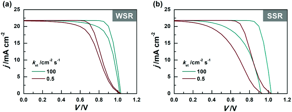 | ||
| Fig. 7 Effects of the charge transfer rate constant (ket) on j–V hysteresis for the PSC limited by radiative and surface recombination. The rate constant of radiative recombination is 6 × 10⁻¹⁰ cm3 s−1. Symbols “WSR” and “SSR” indicate weak and strong surface recombination, respectively. | ||
Conclusions
In summary, the j–V responses for PSCs with different charge extraction properties are simulated by combining drift–diffusion (D–D) equations with a generalized interfacial charge transfer model. In this model, interfacial charge transfer is assumed to be driven by the difference in the Fermi-level at the perovskite/electron selective layer (ESL) boundary. The simulation results indicate an evident hysteresis phenomenon by reducing the charge extraction rate constant even though the recombination is rather weak. This result is attributed to the accumulation of charge carriers and movable ions at the perovskite/ESL contact. Charge accumulation is shown to be associated with the depletion of charge carriers in the ESL. Interestingly, the redistribution of charge carriers induced by limiting charge extraction is found to engender an evident hysteresis loop without additional ion accumulation. Moreover, a loss of open circuit voltage is observed by introducing surface recombination into simulations. It highlights the role of the charge extraction property and reduction of the surface recombination rate in suppressing j–V hysteresis and hence improving the device performance.Conflicts of interest
There are no conflicts to declare.Acknowledgements
We gratefully acknowledge the financial support from the National Natural Science Foundation of China (No. 21103123, 21576215, 21671148), and the Tianjin Natural Science Foundation (18JCZDJC97000).Notes and references
- J.-P. Correa-Baena, A. Abate, M. Saliba, W. Tress, T. Jesper Jacobsson, M. Grätzel and A. Hagfeldt, Energy Environ. Sci., 2017, 10, 710–727 RSC.
- M. Grätzel, Nat. Mater., 2014, 13, 838–842 CrossRef PubMed.
- https://www.nrel.gov/pv/assets/pdfs/best-research-cell-efficiencies.20190923.pdf .
- Y. Cao, Y. Saygili, A. Ummadisingu, J. Teuscher, J. Luo, N. Pellet, F. Giordano, S. M. Zakeeruddin, J. E. Moser, M. Freitag, A. Hagfeldt and M. Grätzel, Nat. Commun., 2017, 8, 15390 CrossRef.
- J.-P. Correa-Baena, M. Saliba, T. Buonassisi, M. Grätzel, A. Abate, W. Tress and A. Hagfeldt, Promises and Challenges of Perovskite Solar Cells, Science, 2017, 358, 739–744 CrossRef CAS PubMed.
- I. Mora-Seró, Joule, 2018, 2, 585–587 CrossRef.
- J. Burschka, N. Pellet, S.-J. Moon, R. Humphry-Baker, P. Gao, M. K. Nazeeruddin and M. Grätzel, Nature, 2013, 499, 316–319 CrossRef CAS PubMed.
- K. Miyano, N. Tripathi, M. Yanagida and Y. Shirai, Acc. Chem. Res., 2016, 49, 303–310 CrossRef CAS.
- J. P. Correa Baena, L. Steier, W. Tress, M. Saliba, S. Neutzner, T. Matsui, F. Giordano, T. J. Jacobsson, A. R. Srimath Kandada, S. M. Zakeeruddin, A. Petrozza, A. Abate, M. K. Nazeeruddin, M. Grätzel and A. Hagfeldt, Energy Environ. Sci., 2015, 8, 2928–2934 RSC.
- B. Dou, J. B. Whitaker, K. Bruening, D. T. Moore, L. M. Wheeler, J. Ryter, N. J. Breslin, J. J. Berry, S. M. Garner, F. S. Barnes, S. E. Shaheen, C. J. Tassone, K. Zhu and M. F. A. M. van Hest, ACS Energy Lett., 2018, 3, 2558–2565 CrossRef CAS.
- M. T. Hörantner, T. Leijtens, M. E. Ziffer, G. E. Eperon, M. G. Christoforo, M. D. McGehee and H. J. Snaith, ACS Energy Lett., 2017, 2, 2506–2513 CrossRef.
- A. Rajagopal, R. J. Stoddard, S. B. Jo, H. W. Hillhouse and A. K. Jen, Nano Lett., 2018, 18, 3985–3993 CrossRef CAS PubMed.
- C. S. Jiang, M. Yang, Y. Zhou, B. To, S. U. Nanayakkara, J. M. Luther, W. Zhou, J. J. Berry, J. van de Lagemaat, N. P. Padture, K. Zhu and M. M. Al-Jassim, Nat. Commun., 2015, 6, 8397 CrossRef CAS PubMed.
- S. A. L. Weber, I. M. Hermes, S.-H. Turren-Cruz, C. Gort, V. W. Bergmann, L. Gilson, A. Hagfeldt, M. Graetzel, W. Tress and R. Berger, Energy Environ. Sci., 2018, 11, 2404–2413 RSC.
- C. Xiao, C. Wang, W. Ke, B. P. Gorman, J. Ye, C. S. Jiang, Y. Yan and M. M. Al-Jassim, ACS Appl. Mater. Interfaces, 2017, 9, 38373–38380 CrossRef CAS PubMed.
- I. M. Hermes, Y. Hou, V. W. Bergmann, C. J. Brabec and S. A. L. Weber, J. Phys. Chem. Lett., 2018, 9, 6249–6256 CrossRef CAS PubMed.
- H. J. Snaith, A. Abate, J. M. Ball, G. E. Eperon, T. Leijtens, N. K. Noel, S. D. Stranks, J. T. Wang, K. Wojciechowski and W. Zhang, J. Phys. Chem. Lett., 2014, 5, 1511–1515 CrossRef CAS PubMed.
- W. Tress, N. Marinova, T. Moehl, S. M. Zakeeruddin, M. K. Nazeeruddin and M. Grätzel, Energy Environ. Sci., 2015, 8, 995–1004 RSC.
- C. Wang, C. Xiao, Y. Yu, D. Zhao, R. A. Awni, C. R. Grice, K. Ghimire, I. Constantinou, W. Liao, A. J. Cimaroli, P. Liu, J. Chen, N. J. Podraza, C.-S. Jiang, M. M. Al-Jassim, X. Zhao and Y. Yan, Adv. Energy Mater., 2017, 7, 1700414 CrossRef.
- B. Chen, M. Yang, X. Zheng, C. Wu, W. Li, Y. Yan, J. Bisquert, G. Garcia-Belmonte, K. Zhu and S. Priya, J. Phys. Chem. Lett., 2015, 6, 4693–4700 CrossRef CAS.
- D. Y. Son, S. G. Kim, J. Y. Seo, S. H. Lee, H. Shin, D. Lee and N. G. Park, J. Am. Chem. Soc., 2018, 140, 1358–1364 CrossRef CAS PubMed.
- K. Wojciechowski, S. D. Stranks, A. Abate, G. Sadoughi, A. Sadhanala, N. Kopidakis, G. Rumbles, C.-Z. Li, R. H. Friend, A. K.-Y. Jen and H. J. Snaith, ACS Nano, 2014, 8, 12701–12709 CrossRef CAS PubMed.
- Y. Li, Y. Zhao, Q. Chen, Y. M. Yang, Y. Liu, Z. Hong, Z. Liu, Y. T. Hsieh, L. Meng, Y. Li and Y. Yang, J. Am. Chem. Soc., 2015, 137, 15540–15547 CrossRef CAS PubMed.
- H. Li, W. Shi, W. Huang, E. P. Yao, J. Han, Z. Chen, S. Liu, Y. Shen, M. Wang and Y. Yang, Nano Lett., 2017, 17, 2328–2335 CrossRef CAS PubMed.
- S.-H. Turren-Cruz, M. Saliba, M. T. Mayer, H. Juárez-Santiesteban, X. Mathew, L. Nienhaus, W. Tress, M. P. Erodici, M.-J. Sher, M. G. Bawendi, M. Grätzel, A. Abate, A. Hagfeldt and J.-P. Correa-Baena, Energy Environ. Sci., 2018, 11, 78–86 RSC.
- J. M. Foster, H. J. Snaith, T. Leijtens and G. Richardson, SIAM J. Appl. Math., 2014, 74, 1935–1966 CrossRef.
- S. van Reenen, M. Kemerink and H. J. Snaith, J. Phys. Chem. Lett., 2015, 6, 3808–3814 CrossRef CAS PubMed.
- H. Xue, K. Fu, L. H. Wong, E. Birgersson and R. Stangl, J. Appl. Phys., 2017, 122, 083105 CrossRef.
- P. Lopez-Varo, J. A. Jiménez-Tejada, M. García-Rosell, J. A. Anta, S. Ravishankar, A. Bou and J. Bisquert, ACS Energy Lett., 2017, 2, 1450–1453 CrossRef CAS.
- P. Calado, A. M. Telford, D. Bryant, X. Li, J. Nelson, B. C. O'Regan and P. R. Barnes, Nat. Commun., 2016, 7, 13831 CrossRef CAS PubMed.
- G. Richardson, S. E. J. O’Kane, R. G. Niemann, T. A. Peltola, J. M. Foster, P. J. Cameron and A. B. Walker, Energy Environ. Sci., 2016, 9, 1476–1485 RSC.
- M. T. Neukom, S. Züfle, E. Knapp, M. Makha, R. Hany and B. Ruhstaller, Sol. Energy Mater. Sol. Cells, 2017, 169, 159–166 CrossRef CAS.
- T. S. Sherkar, C. Momblona, L. Gil-Escrig, J. Avila, M. Sessolo, H. J. Bolink and L. J. A. Koster, ACS Energy Lett., 2017, 2, 1214–1222 CrossRef CAS PubMed.
- N. E. Courtier, J. M. Cave, J. M. Foster, A. B. Walker and G. Richardson, Energy Environ. Sci., 2019, 12, 396–409 RSC.
- D. A. Jacobs, Y. Wu, H. Shen, C. Barugkin, F. J. Beck, T. P. White, K. Weber and K. R. Catchpole, Phys. Chem. Chem. Phys., 2017, 19, 3094–3103 RSC.
- D. Walter, A. Fell, Y. Wu, T. Duong, C. Barugkin, N. Wu, T. White and K. Weber, J. Phys. Chem. C, 2018, 122, 11270–11281 CrossRef CAS.
- P. P. Altermatt, J. Comput. Electron., 2011, 10, 314–330 CrossRef.
- M. García-Rosell, A. Bou, J. A. Jiménez-Tejada, J. Bisquert and P. Lopez-Varo, J. Phys. Chem. C, 2018, 122, 13920–13925 CrossRef.
- T. S. Sherkar, C. Momblona, L. Gil-Escrig, H. J. Bolink and L. J. A. Koster, Adv. Energy Mater., 2017, 7, 1602432 CrossRef.
- N. E. Courtier, G. Richardson and J. M. Foster, Appl. Math. Model., 2018, 63, 329–348 CrossRef.
- D. L. Scharfetter and H. K. Gummel, IEEE Trans. Electron Devices, 1969, 16, 64–77 Search PubMed.
- R. A. Belisle, W. H. Nguyen, A. R. Bowring, P. Calado, X. Li, S. J. C. Irvine, M. D. McGehee, P. R. F. Barnes and B. C. O'Regan, Energy Environ. Sci., 2017, 10, 192–204 RSC.
- W. Tress, A. Petrich, M. Hummert, M. Hein, K. Leo and M. Riede, Appl. Phys. Lett., 2011, 98, 063301 CrossRef.
- M. F. Aygüler, A. G. Hufnagel, P. Rieder, M. Wussler, W. Jaegermann, T. Bein, V. Dyakonov, M. L. Petrus, A. Baumann and P. Docampo, ACS Appl. Mater. Interfaces, 2018, 10, 11414–11419 CrossRef PubMed.
Footnote |
| † Electronic supplementary information (ESI) available: Physical model and numerical details, effect of the charge transfer rate constant on the photovoltaic performance of PSCs, expression of the open circuit voltage, energy diagram of an operating PSC at short and open circuit, profiles of the electrostatic voltage and the screening of the electric field. See DOI: 10.1039/c9cp05381f |
| This journal is © the Owner Societies 2020 |