
 Open Access Article
 This Open Access Article is licensed under a Creative Commons Attribution-Non Commercial 3.0 Unported Licence
Dipole reorientation and local density of optical states influence the emission of light-emitting electrochemical cells†
Alberto
Jiménez-Solano‡
 a,
Laura
Martínez-Sarti
b,
Antonio
Pertegás
b,
Gabriel
Lozano
*a,
Henk J.
Bolink
*b and
Hernán
Míguez
a
a,
Laura
Martínez-Sarti
b,
Antonio
Pertegás
b,
Gabriel
Lozano
*a,
Henk J.
Bolink
*b and
Hernán
Míguez
a
aInstituto de Ciencia de Materiales de Sevilla, Consejo Superior de Investigaciones Científicas-Universidad de Sevilla, Calle Américo Vespucio 49, 41092, Sevilla, Spain. E-mail: g.lozano@csic.es
bInstituto de Ciencia Molecular (ICMol), Universidad de Valencia, Calle Catedrático José Beltrán 2, 46980, Paterna, Spain. E-mail: henk.bolink@uv.es
First published on 5th November 2019
Abstract
Herein, we analyze the temporal evolution of the electroluminescence of light-emitting electrochemical cells (LECs), a thin-film light-emitting device, in order to maximize the luminous power radiated by these devices. A careful analysis of the spectral and angular distribution of the emission of LECs fabricated under the same experimental conditions allows describing the dynamics of the spatial region from which LECs emit, i.e. the generation zone, as bias is applied. This effect is mediated by dipole reorientation within such an emissive region and its optical environment, since its spatial drift yields a different interplay between the intrinsic emission of the emitters and the local density of optical states of the system. Our results demonstrate that engineering the optical environment in thin-film light-emitting devices is key to maximize their brightness.
Aiming to reduce electricity consumption associated with lighting, novel lamps based on light-emitting diodes (LEDs) emerged during the last years of the last century.1 Well-established technologies, such as white LEDs based on a combination of inorganic blue electroluminescent diodes and phosphors, together with complementary technologies, such as those based on organic molecules or semiconductor nanocrystals, must work together to satisfy our needs in the many different scenarios in which artificial light is demanded.2–4 In this context, light-emitting electrochemical cells (LECs) represent a versatile solution-processed alternative for large area diffuse light sources.5 Electroluminescence (EL) in a LEC originates from an active layer in which emitters, e.g. conjugated polymers, semiconductor nanocrystals, small molecules or transition-metal complexes, and mobile ions are sandwiched between two air-stable electrodes.6–9 Specifically, the region within the active layer from which light is emitted, i.e. the generation zone, varies during the operation of the device since mobile ions cause the electrochemical formation of n- and p-type doped highly conductive regions that grow toward each other as bias is applied.10,11
As with all optoelectronic devices,12,13 light management in LECs is also essential to optimize the emission process. The efficiency of a device to shine light depends on its capability of generating photons in the active layer (ηint) and the effectiveness with which such photons exit the device (ηext). Indeed, on the one hand, ηint is the intrinsic quantum yield of the emitter defined by the ratio between its radiative and total decay rate. It is affected by the local density of optical states (LDOS), which is given by the optical environment of the emitter.13,14 On the other hand, ηext is the extraction efficiency given by the fraction of generated light that is radiated into free space, which is determined by the architecture of the device. A judicious design of the optical environment of the active layer should allow boosting light–matter interaction and thus maximizing the luminous power output of the device.15 Despite its simple device architecture, understanding the dynamics of both injected electrical charges and ions along with the drift of the generation zone with the operation time in LECs presents considerable scientific challenges. Indeed, significant efforts have been made in the last years to unravel the working principle and properties of these emitting devices. In particular, researchers have performed a thorough spectroscopic analysis of the emission of LECs and observed a spectral shift in the emission spectrum, which has been attributed to dynamic changes of the generation zone.16–22 The effects of ionic mobility, dielectric constant, temperature, and local electric field on LEC operation have also been investigated.23–28 Additionally, other works have focused on the development of models that combine optical and electrical characteristics.29–32 At the same time, the electric field that builds up along the active layer during operation must have an effect on the orientation of the light emitting molecules, which should in turn affect the intensity of the extracted radiation. Comprehending the interplay between the effect of the LDOS and that of dipole reorientation as voltage is applied should contribute to shedding some light on the temporal evolution of the intensity and the spectral content of the EL in LECs.
In this paper, we demonstrate that the joint effect of dipole reorientation and the optical environment of the emissive region determines the brightness and the directionality of the device with high precision. Correlation of the temporal evolution of all features of the device electroluminescence with that of the generation zone is unambiguously established. Our study is based on the characterization of a set of LECs based on an Ir-complex as the active material. We measured the angular dependence of the EL of these devices as a function of operation time in a fast and reliable way using an optical setup based on Fourier microscopy. We observed that the emission peak reduces and shifts to shorter wavelengths when the emission angle becomes larger, and as a function of the operation time. To analyse the observed behaviour, we developed a rigorous optical model based on finite-difference time-domain (FDTD). We have simulated the spectral dependence of the power radiated into free space (Pout) by a set of dipoles, whose relative orientation changes with time, embedded in the generation zone as a function of its position in such a region within the active layer. Our results highlight the relevance of tuning the optical environment of active layers in thin-film light-emitting devices in order to optimize their performance.
Materials and methods
Device fabrication
LECs were prepared on top of patterned indium tin oxide (ITO, 15 Ω sq−1) coated glass substrates previously cleaned by subsequent sonication in water with soap, deionized water and 2-propanol baths. After drying with nitrogen, the substrates were placed in a UV Ozone cleaner for 20 minutes. Prior to the deposition of the emitting layer, an 80 nm thick film of poly(3,4-ethylenedioxythiophene):poly(styrenesulfonate) (PEDOT:PSS) (CLEVIOS™ P VP AI 4083, Heraeus) was spin-coated on the glass substrate at 1500 rpm, and then annealed at 150 °C for 15 min. The active layer solution was prepared by dissolving an ionic iridium complex ([Ir(ppy)2(dtb-bpy)][PF6]) and an ionic liquid (1-buthyl-3-methylimidazolium hexafluoridophosphate [BMIM][PF6] (>98.5%, Sigma-Aldrich)) in a molar ratio of 4![[thin space (1/6-em)]](https://www.rsc.org/images/entities/char_2009.gif) :1 in a mixture of butan-2-one and anisole (3:2). The solution was filtered through 0.25 μm pore filters and immediately spin-coated on the substrate at 1000 rpm for 60 s. The devices were then transferred to an inert atmosphere glovebox (<0.1 ppm O2 and H2O), where a layer of aluminium (the top electrode) was thermally deposited onto the devices using an Edwards Auto500 chamber integrated in the glovebox. The layout of the fabricated LECs is: glass/ITO (130 nm)/PEDOT:PSS (80 nm)/Ir complex: JF317 (400 nm)/Al2O3 (5 nm)/Al (80 nm). The 5 nm Al2O3 layer was introduced in the model to account for a thin passivation layer over the Al electrode. The thickness of all films was determined using an Ambios XP-1 profilometer. The active area of each pixel in the devices is 6.534 mm2. LECs were not encapsulated.
:1 in a mixture of butan-2-one and anisole (3:2). The solution was filtered through 0.25 μm pore filters and immediately spin-coated on the substrate at 1000 rpm for 60 s. The devices were then transferred to an inert atmosphere glovebox (<0.1 ppm O2 and H2O), where a layer of aluminium (the top electrode) was thermally deposited onto the devices using an Edwards Auto500 chamber integrated in the glovebox. The layout of the fabricated LECs is: glass/ITO (130 nm)/PEDOT:PSS (80 nm)/Ir complex: JF317 (400 nm)/Al2O3 (5 nm)/Al (80 nm). The 5 nm Al2O3 layer was introduced in the model to account for a thin passivation layer over the Al electrode. The thickness of all films was determined using an Ambios XP-1 profilometer. The active area of each pixel in the devices is 6.534 mm2. LECs were not encapsulated.
Optical characterization
The measurements were performed under ambient conditions. LECs were driven using a pulsed current of 50 A m−2 with a duty cycle of 0.5. Future work might include different driving conditions in order to mitigate the temporal decay of the EL as has already been demonstrated.33 Angle-resolved EL measurements were performed using a back focal plane spectroscopy set-up. This comprised an inverted microscope (Leica, DMI300 M) with a high numerical aperture (NA = 0.75) long working distance objective (100×).The collection spot size is 82 microns in diameter. An optical fiber (100 μm core diameter) connected to a spectrophotometer (Ocean Optics, USB2000 + UV-vis) scanned the plane across its diameter. We performed EL measurements right after the current was applied. We also measured different areas of the same device and observed no significant difference.
Numerical modelling
Luminous power radiated into free space by the emitting device (Pout) was modelled using a collection of dipoles oriented along the three main axes as Pout = α·Px + β·Py + γ·Pz, where Px, Py or Pz is the power radiated into free space by a dipole oriented along the x, y or z axis, respectively; and α, β or γ is the relative weight of each contribution with α + β + γ = 1. Notice that for a collection of randomly oriented dipoles, α = β = γ = 1/3. The calculations were done with a commercial FDTD code (Lumerical Inc.).34 A set of single-wavelength simulations was performed with a simulation box size of 2 × 2 × 1 μm3 with perfectly matched layer conditions on every boundary. The mesh grid was set to 10 nm in the x and y axes and 5 nm along the z direction over the entire simulation volume. A 2D frequency-domain field monitor was used to calculate the spatial distribution of the local electric field intensity. The far-field projection, via Fourier transform, was used to propagate the outgoing radiation to a hemisphere at a distance of 1 m. Also, we used an optimization code based on genetic algorithms (GAs) to determine the set that fits the experimental data. In order to minimize the dependence on the initial conditions and its stochastic evolution, the optimization process was repeated 28 times with different initial populations of 27 members. To ensure a faster convergence, the 23 strongest individuals are guaranteed to survive for the next generation. The process was run until the goodness-of-fit function ( , where fi and yi are simulated and experimental data, respectively) stabilized (ε < 10−6) or the maximum number of generations (106) was reached. However, the later stopping criterion was never reached with these conditions. The optical constants of the different materials involved in the calculations are shown in the ESI† (Fig. S1).
Results and discussion
Fig. 1a shows the layout of a LEC in which a 400 nm-thick active layer based on an Ir-complex is sandwiched between a transparent anode (PEDOT:PSS), deposited over ITO coated glass by solution processing, and an Al2O3/Al cathode. The measured photoluminescence (PL) spectra of the Ir-complex both deposited over a glass substrate and when integrated in a more complex optical environment as the one provided by the architecture of a LEC are depicted in Fig. 1b as blue and red lines, respectively. Notice that the PL of the homogenous layer on glass peaks at λ = 594 nm, while the one sandwiched within the device does so at λ = 572 nm, already providing an excellent example of the importance of considering the environment of the emitter when analysing the optical properties of thin-film light-emitting devices, as has been pointed out before.13 Indeed, our simulations, based on considering a collection of light emitting dipoles randomly distributed throughout the active layer, show that this blue shift can be explained by the different LDOS that dipoles experience in each configuration, assuming the presence of the PEDOT:PSS layer does not affect the arrangement of the emitting complexes in the layer. | ||
| Fig. 1 (a) Schematic layout of the light-emitting electrochemical cell (LEC) in which all layers comprising the device are highlighted. (b) Photoluminescence spectra of a layer of the active material (Ir complex JF317) deposited over glass (blue) and embedded in a LEC (red) upon excitation with 450 nm (blue) light. Simulated emission intensity of a collection of isotropic dipoles distributed over the full active layer of the LEC (dashed red). Intrinsic spectral dependence of the intensity radiated by dipoles considered in the calculations (gray). | ||
To evaluate the impact of LDOS on the EL of LECs, we characterize its angular dependence for several devices using reciprocal space imaging, as explained in the Materials and methods section. LECs were driven using a pulsed current source since non-steady state driving slows down the growth of doped zones and thus improves the stability of the emission. Fig. 2a shows the angular dependence of the EL spectra of a representative device. Results of the characterization of other devices are shown in the ESI† (Fig. S2). Measurements reveal a close-to-Lambertian angular emission profile for this planar device. Interestingly, a small blue shift in the maximum of the EL is observed when comparing the spectra measured at a direction close to the normal with that measured at a larger angle (θ = 36 deg), λ = 579 nm vs. λ = 575 nm. Additionally, upon applied bias, the EL spectra further shift to shorter wavelengths and reduce in intensity with operation time, as Fig. 2b displays. However, both the spectral shift and the decrease in EL intensity are fully reversible after turning off the device. These observations are reproducible over the full set of devices characterized (Fig. S2, ESI†).
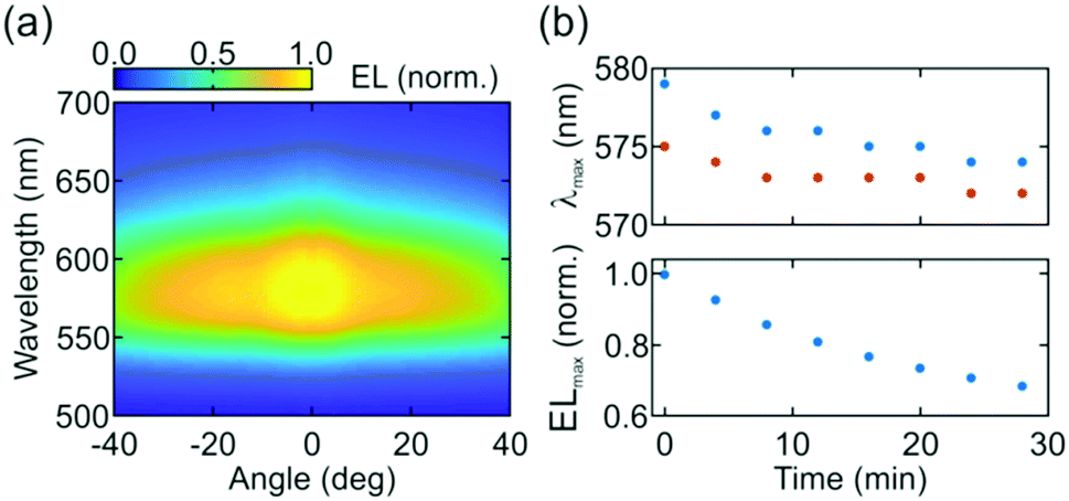 | ||
| Fig. 2 (a) Electroluminescence (EL) spectra as a function of the emission angle for a light-emitting electrochemical cell. (b) Top panel: Spectral position of the maximum of the measured EL spectra as a function of the operation time, for two angles of emission: 11 deg (blue) and 36 deg (red symbols). Bottom panel: Maximum EL intensity at 11 deg as a function of the operation time. | ||
In order to shed some light on the origin of this spectral shift, we simulate the power radiated by randomly oriented dipoles embedded in the 400 nm-thick active layer of a LEC using FDTD. Fig. 3a shows the spectral dependence of Pout of such a dipole depending on its exact position within the active layer. Bright spots in the map reveal the spatial positions at which power radiated into free space is maximized, which highlights the influence of the LDOS. Notice that the number of bright spots in the map is directly related to the thickness of the active layer and originates from interference effects. In particular, calculations (not shown) indicate that a 200 nm-thick active layer only fits one mode and therefore yields a sole maximum of Pout. In order to model the emission in LECs, we assume that the EL of the device originates from a collection of dipoles emitting within the generation zone according to a Gaussian distribution defined by the parameters μ and σ, which relate to the mean value and the full width at half maximum 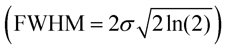 of the distribution, respectively. Notice that μ represents the central position of the generation zone, whereas σ is proportional to the width of such a region. We use an optimization code based on a genetic algorithm to vary both parameters μ and σ, along with γ that relates to the reorientation of dipoles along the z-axis, in order to fit simultaneously the angular and the spectral distribution of the EL intensity for each operation time. As a result, we obtain a Gaussian distribution with μ = 270 nm and σ = 37 nm – see grey curve in Fig. 3a – that defines the generation zone of the LEC at the initial time. The model reveals that the generation zone is slightly displaced from the center towards the cathode and its width is roughly one tenth of the total thickness of the active layer (400 nm), which agrees with previous observations.6,13 Notice that the delicate interplay between conductivities and mobilities of the n- and p-doped regions along with that of the undoped regions determines the position of the generation zone, which may move towards the cathode (or the anode) when the conductivity of the p type layer increases more rapidly than that of the n-type layer (or viceversa). FDTD calculations of the full angular distribution of Pout of dipoles distributed over such a generation zone are shown in the ESI† (Fig. S2). Fitting measurements at different operation times allow extracting the temporal evolution of the generation zone and the fraction of dipoles oriented along the z-axis, and therefore to simulate the angular dependence of the EL intensity with time. Fig. 3b displays the time evolution of the generation zone. Our model shows that the emissive region moves a few nanometers to the anode as it slightly broadens with the operation time. Fig. 3c shows that the relative contribution of dipoles oriented along the z-axis to Pout increases from γ = 0.33 to γ = 0.60. This indicates that the dipoles gradually line up with the external electric field as bias is applied, which causes a significant reduction in the EL intensity since dipoles oriented along the z-axis mainly radiate in the xy-plane. Calculations reproduce: (i) the blue shift of the EL with the emission angle observed experimentally, which originates from the change in location where light is generated with time, and (ii) the decrease in EL intensity with time associated with the reorientation of dipoles. Indeed, Fig. 3d displays such a temporal evolution for maximum Pout, and the spectral position at which this value is attained for two different angles, i.e. θ = 11 deg and θ = 36 deg. Fair agreement is found between measurements and calculations, as further illustrated in Fig. 3e–f, where EL spectra at two different times (t = 0 min and t = 28 min) and two different angles (θ = 11 deg and θ = 36 deg) are plotted (colored lines) along with their corresponding fittings (grey lines). Electrical impedance spectroscopy analysis would provide an alternative way to confirm some of the observations extracted from the optical model.
 | ||
| Fig. 3 (a) Finite-difference time-domain simulation of the spectral dependence of the power radiated into free space (Pout) by a randomly oriented dipole embedded in the active layer of a light-emitting electrochemical cell as a function of its position in such a layer. Gray line represents the generation zone at t = 0 min. Positions z = 0 nm and z = 400 nm represent the interfaces between the active layer and the layer of PEDOT:PSS and Al2O3/Al, respectively. (b) Time evolution of the generation zone. (c) Time evolution of the fraction of dipoles oriented along the z-axis (γ). Dashed gray line is a guide to the eye. (d) Top panel: Spectral position of the maximum calculated Pout as a function of the operation time, for two angles of emission: 11 deg (blue) and 36 deg (red symbols). Bottom panel: Maximum calculated Pout spectra at 11 deg as a function of the operation time. (e and f) Electroluminescence spectra calculated (gray lines) and measured (colored lines) from a LEC device at two different times (t): i.e. t = 0 min (c) and t = 28 min (d) for two different emission angles: 11 deg (blue) and 36 deg (red). | ||
From this analysis, it is clear that the change in the position of the generation zone entails a modification of the optical environment of the emitters, which yields different emission characteristics of the device. In the ESI† (Fig. S3), we show some numerical examples of how the emission of the LEC would change as a function of the generation zone position. In particular, we find a 1.36-fold emission enhancement if light is generated in the spectral region where the LDOS is higher. Our results, thus, open a path to engineer the layout of thin-film light-emitting devices aiming to maximize their performance.
Conclusions
We have performed a thorough analysis of the angular and spectral dependence of the electroluminescence of archetype light-emitting electrochemical cells, employing ionic iridium complexes as the active components. With operation time, we observed a reduction in the electroluminescence intensity, along with a spectral shift with the emission angle, which we attribute to the interplay between dipole orientation and the modification of the spatial region in which light is generated in the device, i.e. the generation zone. We develop a rigorous optical model based on the luminous power radiated into free space by dipoles distributed over the generation zone that gradually line up with the external field. We conclude that dipole reorientation is mainly responsible for the electroluminescence intensity reduction experienced by the devices with operation time whereas the shift of the generation zone as bias is applied determines both the spectral content and the directionality of such emission. Our results demonstrate the relevance of engineering the local density of optical states in thin-film light-emitting devices in order to maximize light–matter interaction and therefore improve their efficiency.Conflicts of interest
There are no conflicts to declare.Acknowledgements
This project has received funding from the European Research Council (ERC) under the European Union's Horizon 2020 research and innovation programme (NANOPHOM, grant agreement no. 715832), and the Spanish Ministry of Economy and Competitiveness via the Unidad de Excelencia María de Maeztu MDM-2015-0538 and under grants, MAT2017-88821-R, and MAT2017-88584-R.References
- S. Pimputkar, J. S. Speck, S. P. DenBaars and S. Nakamura, Nat. Photonics, 2009, 3, 180–182 CrossRef CAS.
- J. Y. Tsao, M. H. Crawford, M. E. Coltrin, A. J. Fisher, D. D. Koleske, G. S. Subramania, G. T. Wang, J. J. Wierer and R. F. Karlicek Jr, Adv. Opt. Mater., 2014, 2, 809–836 CrossRef CAS.
- S. Reineke, Nat. Mater., 2015, 14, 459–462 CrossRef CAS PubMed.
- G. Lozano, J. Phys. Chem. Lett., 2018, 9, 3987–3997 CrossRef CAS PubMed.
- S. Tang, A. Sandström, P. Lundberg, T. Lanz, C. Larsen, S. van Reenen, M. Kemerink and L. Edman, Nat. Commun., 2017, 8, 1190 CrossRef PubMed.
- S. B. Meier, D. Tordera, A. Pertegás, C. Roldán-Carmona, E. Ortí and H. J. Bolink, Mater. Today, 2014, 17, 217–223 CrossRef CAS.
- S. Tang and L. Edman, Top. Curr. Chem., 2016, 374, 40 CrossRef PubMed.
- E. Fresta and R. D. Costa, J. Mater. Chem. C, 2017, 5, 5643–5675 RSC.
- J. Xu, A. Sandström, E. M. Lindh, W. Yang, S. Tang and L. Edman, ACS Appl. Mater. Interfaces, 2018, 10, 33380–33389 CrossRef CAS PubMed.
- Y. Hu and J. Gao, J. Am. Chem. Soc., 2011, 133, 2227–2231 CrossRef CAS PubMed.
- Z. Yu, M. Wang, G. Lei, J. Liu, L. Li and Q. Pei, J. Phys. Chem. Lett., 2011, 2, 367–372 CrossRef CAS.
- S.-F. Leung, Q. Zhang, F. Xiu, D. Yu, J. C. Ho, D. Li and Z. Fan, J. Phys. Chem. Lett., 2014, 5, 1479–1495 CrossRef CAS PubMed.
- A. Jiménez-Solano, J. F. Galisteo-López and H. Míguez, J. Phys. Chem. Lett., 2018, 9, 2077–2084 CrossRef PubMed.
- A. F. Koenderink, A. Alu and A. Polman, Science, 2015, 348, 516–521 CrossRef CAS PubMed.
- L. Novotny and B. Hecht, Principles of Nano-Optics, Cambridge University Press, Cambridge, UK, 2006 Search PubMed.
- Y.-P. Jhang, H.-F. Chen, H.-B. Wua, Y.-S. Yeh, H.-C. Su and K.-T. Wong, Org. Electron., 2013, 14, 2424–2430 CrossRef CAS.
- T.-W. Wang and H.-C. Su, Org. Electron., 2013, 14, 2269–2277 CrossRef CAS.
- G.-R. Lin, H.-F. Chen, H.-C. Shih, J.-H. Hsu, Y. Chang, C.-H. Chiu, C.-Y. Cheng, Y.-S. Yeh, H.-C. Su and K.-T. Wong, Phys. Chem. Chem. Phys., 2015, 17, 6956–6962 RSC.
- S. Jenatsch, L. Wang, M. Bulloni, A. C. Véron, B. Ruhstaller, S. Altazin, F. Nüesch and R. Hany, ACS Appl. Mater. Interfaces, 2016, 8, 6554–6562 CrossRef CAS PubMed.
- S. Jenatsch, M. Regnat, R. Hany, M. Diethelm, F. Nüesch and B. Ruhstaller, ACS Photonics, 2018, 5, 1591–1598 CrossRef CAS.
- E. M. Lindh, P. Lundberg, T. Lanz, J. Mindemark and L. Edman, Sci. Rep., 2018, 8, 6970 CrossRef PubMed.
- M. Diethelm, Q. Grossmann, A. Schiller, E. Knapp, S. Jenatsch, M. Kawecki, F. Nüesch and R. Hany, Adv. Opt. Mater., 2019, 7, 1801278 CrossRef.
- J. D. Slinker, J. A. DeFranco, M. J. Jaquith, W. R. Silveira, Y.-W. Zhong, J. M. Moran-Mirabal, H. G. Craighead, H. D. Abruña, J. A. Marohn and G. G. Malliara, Nat. Mater., 2007, 6, 894 CrossRef CAS PubMed.
- K. J. Suhr, L. D. Bastatas, Y. Shen, L. A. Mitchell, B. J. Holliday and J. D. Slinker, ACS Appl. Mater. Interfaces, 2016, 8, 8888 CrossRef CAS PubMed.
- M. D. Weber, J. E. Wittmann, A. Burger, O. B. Malcıoğlu, J. Segarra-Martí, A. Hirsch, P. B. Coto, M. Bockstedte and R. D. Costa, Adv. Funct. Mater., 2016, 26, 6737 CrossRef CAS.
- M. Kawecki, R. Hany, M. Diethelm, S. Jenatsch, Q. Grossmann, L. Bernard and H. J. Hug, ACS Appl. Mater. Interfaces, 2018, 10, 39100 CrossRef CAS PubMed.
- M. H. Bowler, T. Guo, L. D. Bastatas, M. D. Moore, A. V. Malko and J. D. Slinker, Mater. Horiz., 2017, 4, 657 RSC.
- L. D. Bastatas, M. D. Moore and J. D. Slinker, ChemPlusChem, 2018, 83, 266 CrossRef CAS.
- I. H. Campbell, D. L. Smith, C. J. Neef and J. P. Ferraris, Appl. Phys. Lett., 1998, 72, 2565 CrossRef CAS.
- S. van Reenen, P. Matyba, A. Dzwilewski, R. A. J. Janssen, L. Edman and M. Kemerink, J. Am. Chem. Soc., 2010, 132, 13776 CrossRef CAS PubMed.
- A. Munar, A. Sandström, S. Tang and L. Edman, Adv. Funct. Mater., 2012, 22, 1511 CrossRef CAS.
- E. M. Lindh, P. Lundberg, T. Lanz and L. Edman, Sci. Rep., 2019, 9, 10433 CrossRef PubMed.
- D. Tordera, S. Meier, M. Lenes, R. D. Costa, E. Ortí, W. Sarfert and H. J. Bolink, Adv. Mater., 2012, 24, 897 CrossRef CAS PubMed.
- L. Solutions, Inc. http://www.lumerical.com/tcad-products/fdtd/.
Footnotes |
| † Electronic supplementary information (ESI) available: Optical constants of materials involved in the calculations, EL measurements of fabricated devices and numerical results. See DOI: 10.1039/c9cp05505c |
| ‡ Max Planck Institute for Solid State Research, Heisenbergstraße 1, 70569 Stuttgart, Germany. |
| This journal is © the Owner Societies 2020 |