
Mixed 4f population of Tm adatoms on insulating Cu2N islands
David
Coffey†
*abc,
César
de la Fuente
bc,
Miguel
Ciria
 bc,
David
Serrate
bc,
Sebastian
Loth
def and
José Ignacio
Arnaudas
ac
bc,
David
Serrate
bc,
Sebastian
Loth
def and
José Ignacio
Arnaudas
ac
aLaboratorio de Microscopías Avanzadas, Instituto de Nanociencia de Aragón, Universidad de Zaragoza, Zaragoza, Spain. E-mail: coffeyLPM@leidenprobemicroscopy.com
bInstituto de Ciencia de Materiales de Aragón, Consejo Superior de Investigaciones Científicas, Zaragoza, Spain
cDepartamento de Física de la Materia Condensada, Universidad de Zaragoza, Zaragoza, Spain
dMax Planck Institute for Solid State Research, 70569 Stuttgart, Germany
eMax Planck Institute for the Structure and Dynamics of Matter, 22761 Hamburg, Germany
fInstitute for Functional Matter and Quantum Technologies, University of Stuttgart, 70569 Stuttgart, Germany
First published on 18th November 2019
Abstract
The electronic properties of Tm and Lu atoms adsorbed on nanoscale Cu2N insulating islands and on a clean Cu(100) surface have been investigated by scanning tunnelling microscopy and spectroscopy, and density functional calculations modelling the electronic structure of the rare earth atoms were performed. While Lu adatoms display the same spectra on both surfaces, tunnelling spectra of Tm on Cu2N indicate a state at ≃0.8 V or ≃1.9 V bias, depending on the 4f population of the adatom, 4f12 or 4f13, which is not present on Tm atoms adsorbed on Cu(100). Although inelastic 4f-spin-flip excitations were not detected, variation of tunnelling through the strongly correlated d-electrons indicates that the insulating layer opens a pathway to access the electronic state of those 4f electrons in the single adatom.
1 Introduction
The study of structures comprising a few or a single atom is of importance from a fundamental physics point of view, however the experimental realization and characterization of such structures can be challenging. Clean metal surfaces are the most usual substrates for STM experiments and are particularly suited for atomic manipulation and the construction of artificial structures, as the low diffusion barriers of adsorbed atoms and molecules and flat surface potential of the metal allow for reproducible lateral atomic manipulation; however, the counterpart is that metals might not be the ideal substrate for the investigation of the electronic properties of said atoms and structures, as their orbitals will strongly couple with the surface state of metals. Although a fully insulating substrate is not a valid sample for tunnelling experiments, an intermediate situation consisting of a thin insulating film grown on a conductive sample has been proven to be a viable and fruitful avenue for local probe experiments.1The role of the insulating layer is to electronically decouple adsorbed atoms and molecules from the metallic substrate.2 This opens several interesting routes for research, as, to name a few, in the new situation molecular bonds that were previously hybridised will retain their discrete energy levels and allow their orbitals to be imaged by STM,3 lifetimes of quantum states can improve significantly due to the closure of decay paths involving scattering with substrate electrons,4 or the charge state of a single atom can be controlled, charging and discharging a single electron.5 The increased anisotropy introduced by a thin insulating layer can be used to enhance single-atom spin flip spectroscopy, too, as has been done to the great effect on 3d atoms.6,7 In recent years the study of rare-earth elements has come to the foreground, after it was shown that holmium adatoms on magnesium oxide behave as bistable single atom magnets at low temperatures.8 Using spin-polarized STM, the stability of the spin state of a single Ho adatom9 and the means to control it10 have been investigated; the adsorption sites were also precisely identified.11 However, on Cu2N, experimental results are limited to Ce adatoms,12,13 while theoretical studies investigated Gd adatoms and dimers on CuN/Cu substrates.14 The electronic structure of rare earths differs from that of transition metals in the 4f electron shell, incomplete in the case of rare earths (RE), except for Lu, while for transition metals it is either empty, as in lighter 3d and 4d elements, or complete in the case of heavier 5d metals. Accessing these states is an area of open research in single atoms10,15–18 and molecules with RE centres,19–22 as they have great interest for technological applications as single-atoms8 or single-molecule magnets.23 Apart from STM, other approaches have been used, particularly XMCD,8,24–28 to explore the electronic and magnetic properties of single rare earth adatoms on different metallic surfaces.
In this work two different rare-earth species, Tm and Lu, are studied as single atoms on a metallic Cu(100) surface and on insulating Cu2N islands grown on it, by performing differential conductance spectroscopy over different energy ranges. The dI/dV curves for Tm/Cu2N present additional resonances compared with Tm/Cu(100), while for Lu adatoms the spectra are featureless for both kinds of substrates. The origin of the electronic features is further explored by first principles calculations, determining that the LDOS of the RE adatoms at these energies have 5d orbital character and are influenced by the incomplete 4f orbitals.
2 Experimental section
2.1 Adatom deposition
The insulating layer used in this research consists of a single atomic layer of Cu2N,29–31 prepared by implanting N atoms on a clean Cu(100) surface. Preparing Cu2N requires first preparing a high quality clean Cu(001) surface, which follows the typical process for noble metals. The surface is cleaned by removing the most external atomic layers by Ar+ sputtering at 1 kV, with PAr ∼ 1 × 10⁻⁶ mbar, followed by annealing under UHV conditions at T ∼ 900 K. By repeated sputtering–annealing cycles, a clean Cu(001) surface can be produced. Nitrogen atoms are implanted on the Cu surface by sputtering in a N2 atmosphere. To favour the self-assembly of regular islands, the sputtering process is followed by a gentler annealing process than for the clean surface, at T ∼ 600 K.Before dosing rare earth atoms on the sample prior characterization of both Cu(100) and Cu2N surfaces is performed. Fig. 1a shows an STM image of a typical Cu2N sample, and the dI/dV spectra taken over ±3 V on (b) Cu(100) and (c) Cu2N. The Cu2N patches are represented by a darker color in the topography image, as they appear as a 100 pm depression; the increase of dI/dV at 2 V corresponds to the onset of the conduction band.30,32
 | ||
| Fig. 1 (a) Details of a STM image of Cu2N islands on Cu(100) and dI/dV spectra of the two areas, (b) the remaining clean Cu(100) surface and (c) a Cu2N island. | ||
Rare earth atoms were evaporated by e-beam heating a molybdenum crucible filled with 99.99% purity bulk Tm (Lu) onto a cold sample. In the case of Lu the experiment was performed in a SPECS JT system, where the evaporation is performed with the sample at the STM stage, keeping the sample at T = 5 K. In the case of Tm the experiment was performed using a Unisoku 1300 STM, where the sample is loaded vertically into the STM stage inside of the cryostat. The sample and transfer rod were pre-cooled for three hours at the STM stage down to a temperature of 4 K, and the sample is then disengaged from the STM and exposed for a few seconds to a flux of Tm atoms and reinserted.
The topography of the resulting samples can be seen in Fig. 2a for Tm and in Fig. 3a for Lu. Profiles taken on Tm adatoms at 150 mV show a height of 260 pm for adatoms on Cu and 240 pm for adatoms on Cu2N (Fig. 2b and c); profiles on Lu adatoms show a height of 220 pm over Cu(100) and 240 pm over Cu2N (Fig. 3b).
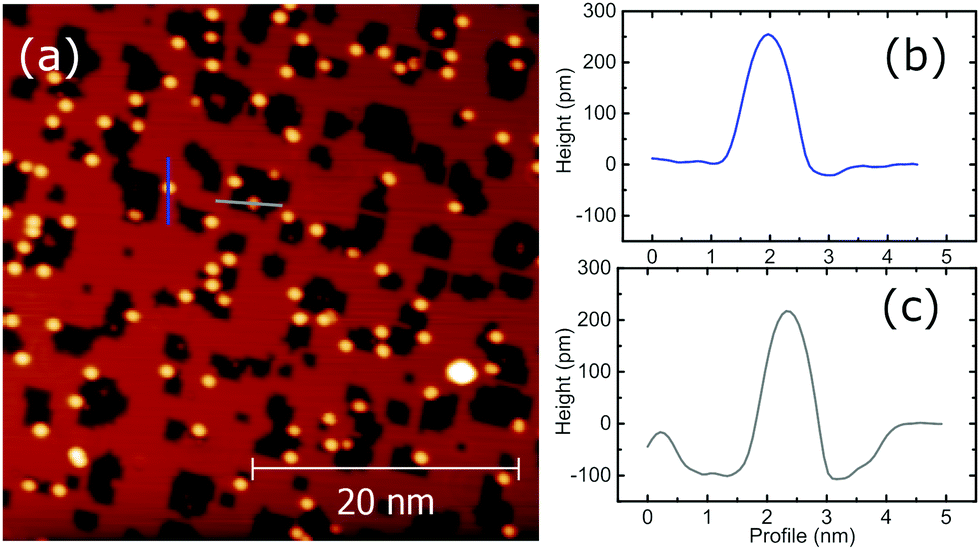 | ||
| Fig. 2 (a) Topography of a Cu2N sample with Tm adatoms, taken at VBias = 150 mV, It = 1 nA. Profiles along the lines over the indicated Tm adatoms: (b) on Cu(100), blue line; and (c) on Cu2N, grey line. | ||
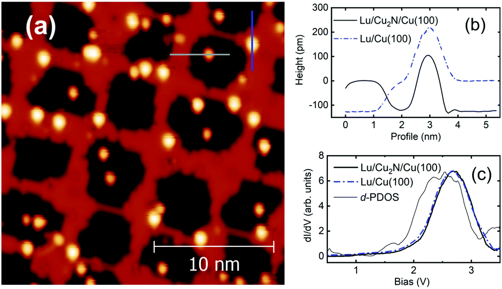 | ||
| Fig. 3 (a) STM image of Lu adatoms on a Cu2N sample (VBias = 100 mV, It = 1 nA). On the right: (b) profiles along the blue line in (a) for a Lu adatom on Cu(100) (dashed–dotted line) and along the gray line in (a) for a Lu adatom on Cu2N (continuous line); (c) representative spectra taken on Lu adatoms on both Cu(100) (dashed–dotted line) and Cu2N (continuous line) from 0.5 to 3.5 V. In this case both species present a very similar behaviour, a single large broad feature centred around 2.6 V, and no other features at lower bias. The thin line is the calculated d-PDOS. | ||
2.2 Spectroscopy on Tm/Cu and Tm/Cu2N
Identification of the adatoms is done by performing dI/dV spectroscopy on different objects over a wide energy range (±3.5 V), both for objects on the Cu(100) surface and for objects on the Cu2N patches. Representative spectra of each case are shown in Fig. 4. Two different behaviours are observed, depending on the substrate: objects on Cu(100) all present similar spectra (Fig. 4a), indicating that they are all the same species, consistent with the objects being single Tm atoms; objects on Cu2N also present similar spectra (Fig. 4b), although different from those observed on Cu. On Cu(100), the spectra of Tm adatoms somewhat resemble the spectra of bare Cu (Fig. 1b); on the other hand, the features are sharper for Tm adatoms on Cu2N, presenting a larger peak at 2.1 V and an additional smaller feature at 0.8 V not observed for adatoms on Cu(100).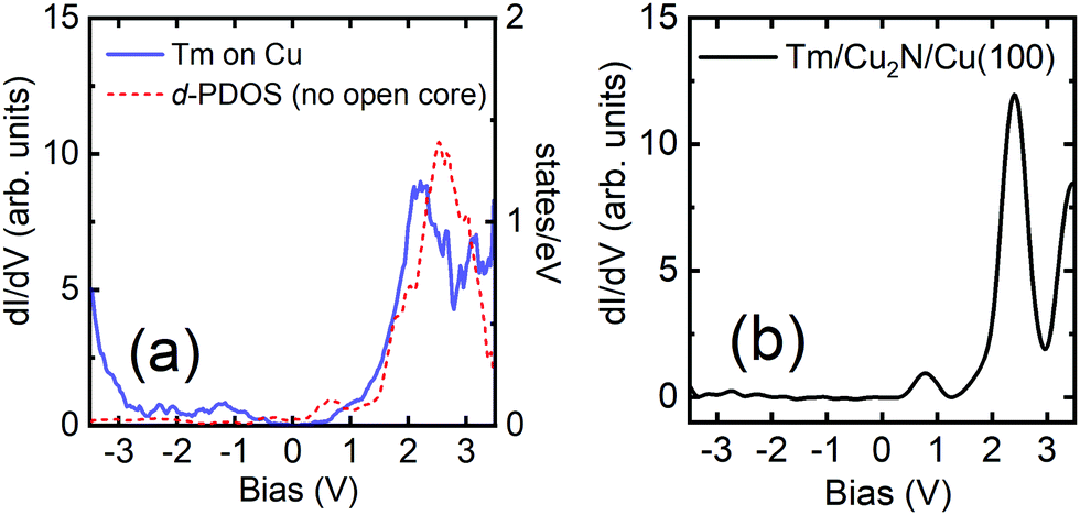 | ||
| Fig. 4 Typical spectra taken on Tm adatoms on (a) Cu(100) and (b) Cu2N. The thin line in (a) represents the calculated d-PDOS. | ||
To ensure that this behaviour is not atom dependent and that objects on Cu(100) and on Cu2N are not, in fact, two different species, Tm adatoms on Cu(100), are vertically manipulated onto Cu2N patches. Vertical manipulation requires moving the atom onto the tip, and then dropping it back to the surface in a controlled fashion. While lateral atom manipulation is the usual approach in metals, it does not work well on insulating layers.2,7 A single Tm adatom on the Cu(100) surface can be reliably picked up onto the tip by regulating over it at VBias = 10 mV, It = 1 nA, disengaging the feedback loop, lowering the tip 300 pm towards the atom and applying a 1 V pulse; conversely, after picking up the Tm atom it can be dropped onto a Cu2N patch by regulating over it at VBias = 10 mV, It = 1 nA, lowering the tip 200 pm towards the surface and applying a −1 V pulse. Fig. 5 shows the topography of a 15 × 15 nm area before and after vertically manipulating several Tm atoms on Cu (indicated by blue circles) onto Cu2N patches (atoms at new positions are indicated by white circles).
 | ||
| Fig. 5 Atom manipulation of Tm adatoms (VBias = 10 mV, It = 1 nA). Atoms were picked up onto the STM tip from the Cu(100) surface, marked in blue, and dropped onto Cu2N islands at the positions marked in grey. The image shows the sample prior to starting and after several successful manipulations. | ||
Prior to manipulation, all the atoms presented the same spectra as shown in Fig. 4a, corresponding to a Tm adatom on Cu(100); however, as shown in Fig. 6, after manipulation onto Cu2N two different spectra can be observed, in one case the same as the spectra corresponding to Tm on Cu2N seen in Fig. 4b, with a large peak at 2.1 V and a smaller feature at 0.8 V, while other adatoms present similar spectra shifted to higher energies: the large peak appears at 2.6 V, while the smaller feature is shifted above 1.5 V.
 | ||
| Fig. 6 Spectra taken on Tm adatoms on Cu(100): (a) prior to manipulation, showing the same behaviour for Tm/Cu(100) as seen in Fig. 4(a), and (b) after vertical manipulation onto Cu2N, showing the same behaviour as seen for Tm/Cu2N in Fig. 4(b). On the other hand, the set of Tm adatoms presented in (c), which also conform to Tm/Cu(100), presents shifted spectra when manipulated onto Cu2N (d). In both (b) and (d) the calculated d and p-PDOS are overlaid with the differential conductivity spectra (see the text for details). | ||
2.3 Spectroscopy on Lu/Cu and Lu/Cu2N
To further investigate whether the observed feature at 0.8 is specific to Tm, the experiment is repeated using lutetium. Lu atoms present a similar electronic configuration to Tm, but with a significant difference of having a full 4f shell. Because of this, 4f electrons will not be able to contribute to the unoccupied LDOS, either while lying on Cu(100) or on Cu2N.Fig. 3c shows representative spectra taken on Lu adatoms on both Cu(100) and Cu2N from 0.5 V to 3.5 V. In this case both species present a very similar behaviour, a single large broad feature centred around 2.6 V, and no other features at lower bias.
The spectroscopic behaviour near EF of Tm and Lu adatoms on Cu2N and Cu(100) is presented in Fig. 7. Even though the electronic configuration of Tm could allow for spin excitations of the 4f orbital produced by the tunnelling current, spectra taken on single Tm adatoms on the Cu(100) surface present no observable signature of inelastic electron tunnelling (IET) (Fig. 7c), or any other distinct feature, nor do the spectra taken on Tm adatoms on Cu2N (Fig. 7d). While the spectra are not flat in the explored range, both are hardly distinguishable within the noise-level from spectra taken on the Cu(100) surface (Fig. 7b), indicating that the shape of the spectra is tip-related, rather than due to the Tm adatoms. A similar behaviour is observed for Lu adatoms (Fig. 7e), a tip-related peak and no IET signature, which in this case would be expected due to the 4f orbital being complete for Lu.
 | ||
| Fig. 7 (a) STM image showing a 6 × 6 nm2 area with Tm adatoms lying on both the Cu(100) and Cu2N surfaces; differential conductance spectra taken over ±20 mV dI/dV, at a base temperature of 0.5 K, using a modulation voltage of 200 μV, on (b) the Cu(100) surface, (c) a Tm adatom on Cu(100), and (d) on a Tm adatom on Cu2N. (e) Differential conductance spectra taken over a ±50 mV range of Lu adatoms on the Cu(100) surface (dashed–dotted line) and the Cu2N surface (continuous line), as well as on the bare Cu(100) surface (dashed line). | ||
3 Density functional calculations
In order to discern the nature and orbital character of the foremost features observed in the STM differential conductivity spectra at the RE adatoms on Cu2N/Cu(100) and on Cu(100), we performed ab initio density functional calculations using the pseudo-potential method with two different 4f electronic populations for the RE adatoms and over all accessible sites of the (100) studied surfaces. It seems reasonable to consider changes in the 4f occupancy of the RE adatoms since it depends not only on an intrinsic atomic quantity, as is the energy needed to change the valence of the ground state, but also on the different binding energies for different states.33–35 The latter is associated with the hybridization of the valence electrons, which also depends on the kind of substrate and on the adsorption site, as it has been recently shown for several RE adatoms deposited on different metallic substrates.26The electronic properties of RE/Cu(100) and RE/Cu2N/Cu(100) are studied by means of ab initio calculations based on DFT as implemented in VASP.36 We use the generalized gradient approximation (GGA) and local spin density approximation (LSDA) for correlation and exchange.37 The rotationally invariant LSDA+U theory, introduced by Liechtenstein et al.,38 has been used for describing the strongly correlated d and f electrons when the GGA fails. The 4f shell occupation for the RE adatoms was introduced in the calculation by selecting the open-core electronic configuration, where 12 f-electrons are in the core and do not show up in the valence region, and a normal electronic configuration where they are free to behave as valence electrons.
After testing the convergence for different supercell-sizes in RE/Cu2N/Cu(100) and RE/Cu(100), we used 224 Cu-atoms in a (4 × 4 × 7)-superstructure oriented along [100] with 32 Cu atoms/layer, a vacuum layer of 35 Å thick, one RE adatom and, for RE/Cu2N/Cu(100), 32 N atoms in the two surface monolayers, having 16 N atoms per surface. A fully 3D ionic relaxation was done for the RE adatoms including the three nearest layers and keeping the central Cu-layer fixed. The ion relaxation was calculated at the Γ-point by using, first, a conjugate-gradient method39 and the quasi-Newton method later.40 Hellmann–Feynman forces are around 1.5 mRy per a.u. per atom. This optimization gives average interlayer distances, along [100], of d(Cu2N–Cu(1)) = 2.08 Å, d(Cu(1)–Cu(2)) = 1.83 Å and d(Cu(2)–Cu(3)) = 1.80 Å for RE/Cu2N/Cu(100). Similar distances between Cu layers are obtained for the RE/Cu(100) case. The rare-earth adatoms are positioned on top of Cu sites in RE/Cu2N/Cu(100) and RE/Cu(100) cases, having an average distance between the RE adatom and the nearby surface of ≃2.3 Å. Tiny displacements toward N-sites were obtained in both systems. The adsorption site agrees with that deduced in ref. 12 from atomically resolved STM images of Ce adatoms on Cu2N, which also protrude from the surface ≃2.2 Å. The RE binding introduces local distortions on the nearest Cu2N or Cu surface, alike those observed for 3d adatoms (see for example ref. 41 and references therein).
For the study of the electronic properties, we used different k-mesh grids under the Monkhorst–Pack scheme42 to check the convergence of calculations and validate the structural model used. However, a (4 × 4 × 1) k-mesh was finally selected because it allowed us to get a better compromise between accuracy and computational efforts. The self-consistent electronic relaxations have an energy precision better than 0.05 meV for an energy cut-off rounding to 350 eV. Dipolar corrections are only included for RE/Cu2N/Cu(100) cases.43,44
For the non-open core configuration, Coulomb repulsion for the f electrons Uff is obtained by the knowledge of the inelastic spin-flip excitations near the Fermi level. The absence of this transition in the dI/dV curves (see Fig. 7c and d) precludes the use of experimental values to adjust the set Uff in the calculation, instead we used the value of Uff obtained from ref. 45 to calculate the f-PDOS for RE adatoms. On the other hand, for the open-core scheme calculations of the PDOS, the LSDA+U correction Udd parameter used was appropriate to fit the differential conductivity experimental data.
In Fig. 8, with blue continuous lines, we display the calculated spin-averaged PDOS: (a) s-PDOS, (b) p-PDOS, (e) d-PDOS and (f) f-PDOS for Tm/Cu2N/Cu(100) by using Uff = 5 eV, where Tm has almost 13 f-electrons after self-consistent electronic relaxation. The f-PDOS has only relevant contributions below the Fermi energy and the d-PDOS shows important contributions above the Fermi energy between 1.8 and 3 eV. On the other hand, the red dotted line plots in (c), (d) and (e) of Fig. 8 represent the calculated s, p and d-PDOS, respectively, for the same Tm adatom on Cu2N/Cu(100) by using Udd = 5 eV. In this calculation, because we use an open-core scheme, the Tm adatom has 12 f-electrons within the Tm-core. The d-PDOS energy distribution is well-centered around 0.8 eV and the p-PDOS shows important contribution above the Fermi energy at around 2.3 eV.
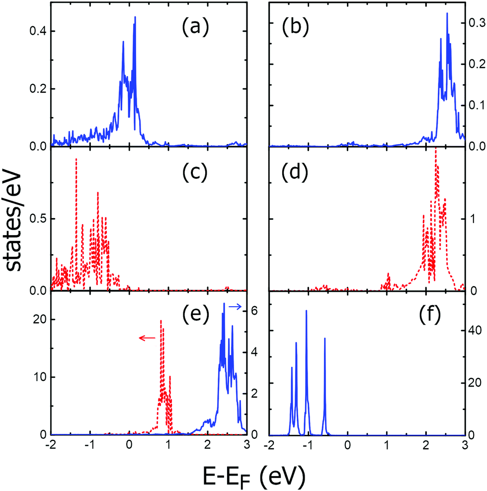 | ||
| Fig. 8 Calculated spin-averaged partial densities of states for Tm in Tm/Cu2N/Cu(100): with continuous lines (blue), (a) s-PDOS, (b) p-PDOS, (e) d-PDOS and (f) f-PDOS, where the Tm adatom has 13 f-electrons; with dotted lines (red), (c) s-PDOS, (d) p-PDOS and (e) d-PDOS, for a Tm adatom with 12 f-electrons. | ||
Similar calculations were performed for Tm/Cu(100) cases using the same Uff and Udd values and the two different 4f configurations (non-open-core and open-core). In these cases, we obtained significant values for the d-PDOS only in the range from +2 to +3 eV, in agreement with the differential conductivity spectra shown in Fig. 4a, but without peaks of the d-PDOS around 0.8 or below 2 eV.
The d-PDOS of the Lu adatom is shown in Fig. 3c for Lu/Cu2N/Cu(100) by using Uff = 5 eV (ref. 45). The same energy distribution of the d-PDOS appears as well for the Lu adatom in Lu/Cu(100) using the same Uff value. Both spectra have close features at around 2.5 eV, near the experimentally observed increases of dI/dV, with Lu adatoms having almost free atom configuration of 14 f-electrons after the convergence of electronic relaxation. However, the d-PDOS calculated for the Lu adatom using an open-core configuration cannot be associated with any of the features observed at positive bias in the differential conductivity spectra presented in the previous section, even using different Udd values.
4 Discussion and conclusions
The local differential conductivity spectra measured on the RE adatoms studied share a common characteristic in all the cases, which is a large peak in the range of 2 to 3 eV (see Fig. 4 and 6 for Tm and Fig. 3c for Lu). However, as shown in Section 2.2, Tm adatoms present additional smaller peaks when they are located on Cu2N islands: at ≃0.8 eV, irrespective of whether they were on the Cu2N island directly after deposition (Fig. 4b) or after being transported to it from the surface of Cu (100) by STM manipulation (Fig. 6b). Additional peaks between ≃1.5 and ≃1.9 eV appeared only for other manipulated adatoms (Fig. 6d).Comparison with DFT calculations shows that the small peak at ≃0.8 eV can be related to the d-states for a Tm adatom in an open-core configuration (12 f-electrons in the core) (see Fig. 8e, dotted line). However, this d-PDOS does not show a relevant increase in the 2–3 eV range. The large single peak observed in the differential conductivity near above 2 eV for these adatoms could not be due to an intrinsic increase of their d-states, but to a resonance of the p-PDOS of the adatom (see Fig. 8d) with the surface d-state of Cu2N existing at 2.2 eV.30,32 This surface state, in turn, may arise from an electronic state at the Cu2N/Cu interface, derived from the Cu(100) surface state localized between 1.4 and 2 eV,46,47 with a shift due to the dielectric layer.30 In Fig. 6b, both the d and p-PDOS of a Tm adatom having 12 f-electrons are overlapped with the differential conductivity spectra measured on several of such kinds of Tm adatoms on Cu2N.
The other kind of spectra, measured on some of the manipulated Tm adatoms (Fig. 6d) and characterized by a small peak slightly below 2 eV, as well as the large split peak between 2 and 3 eV, can be related to the d-PDOS on a Tm adatom with 13 valence f-electrons (the main panel of Fig. 8e, continuous line). In Fig. 6d we have overlaid the d-PDOS and the p-PDOS for a 13 f-electron Tm adatom (Fig. 8b) with the differential conductivity spectra. We find that the d-PDOS fully accounts for the observed features in the differential conductivity.
The shift in energy of the small peaks in the differential conductivity spectra, from 0.8 V to 1.5 V or higher, could be caused by different sources, the two most obvious being a contamination during manipulation or differences in the local environment. Hydrogen contamination, which can be an issue in longer experiments as H adsorbed on the chamber walls desorbs over time, would be expected to produce a difference in the constant current topography of the adatom, as well as a large change in differential conductance spectroscopy,48,49 which does not seem to be the case. Instead, the most likely origin of the shift is due to the adatom being in a different position on the Cu2N lattice and thus in the presence of a different crystal field. Adsorption on different binding sites has been shown to have a very strong effect on the electronic properties of 3d metals.31 Otherwise, for the RE the 4f electrons are highly shielded and thus a feature of the 4f origin would be less affected by changes in the local crystal field than for 3d metals, but it is also known that for RE ions in oxides, fluorides and other compounds with covalent/ionic bonds, due to the interaction with the crystal field, the average position of the 5d levels, i.e., the centroid, is lowered relative to the position for the free ion. This, combined with the crystal field and spin–orbit splitting, results in a decrease of the f → d transition energy.50 In our case, we can fit the different conductivity spectra observed for Tm adatoms by a different population of the 4f orbitals, therefore, although shielded by the 5s and 5p electrons, the 4f electrons appear to be influenced by the adatom environment. In particular, our calculations suggest that the as-deposited Tm adatoms have always 12 4f electrons and, when manipulated at 1 K, may gain one additional electron for the 4f shell. The main difference between the as-deposited adatoms and those manipulated is that, during evaporation, hot Tm adatoms are able to diffuse slightly over the Cu2N surface and reach the binding site of minimum energy; on the other hand, atomic manipulation is performed at 1 K and diffusion is strongly inhibited, and adatoms are more likely to stay in a local minimum of the surface energy potential. Therefore, for the adatoms located at deeper energy minima, it can be energetically favourable to promote a 4f electron to a higher energy shell, but for those sited on local minima, the energy balance leads to a 4f shell with 13 electrons.
The observation that the small peaks at 0.8 V only appear on Cu2N and not on the Cu(100) surface could indicate that in the latter case the Tm adatom hybridizes with the metallic surface in a more uniform way, i.e., the binding energy is similar for the different adsorption sites and the population of the 4f orbitals stays fixed. Specifically, the number of 4f electrons calculated for the Tm adatoms on Cu(100) is ≅13, the same as that obtained by Singha et al. on Cu(111).26
As to the Lu adatoms, the strikingly similar behaviour observed for adatoms in a metallic environment and for adatoms on the insulating layer is surprising, as the substrate had a very noticeable effect on Tm adatoms. This reinforces the idea pointed out above of the effect on the 4f orbital for Tm when it is adsorbed on an insulating layer, as this orbital being complete in Lu but incomplete in Tm is the main electronic difference between the two RE.
Inelastic spin-flip excitation on RE atoms and clusters is of great interest, as their strongly localized 4f states are candidates for long lived atomic magnetic states, which if accessible to IET spectroscopy could be probed unperturbed by tunnelling at energies lower than the excitation threshold, and switched by going over it. There have been multiple studies in the matter, where in some cases positive results have been reported15–17 while in others the absence of any excitation has been explicitly noted,10,18 as is the case for Tm and Lu on Cu2N here reported.
Our study of the electronic properties of Tm and Lu adatoms on a metallic and an insulating surface indicates that the tunnelling electrons access states with d-character and there is no direct access to 4f electrons, or at least none capable of producing a measurable contribution to the LDOS. Moreover, inelastic 4f-spin-flip excitations have not been detected in any case, consistent with negligible direct tunnelling into 4f orbitals. Recent advances in combining STM with electron paramagnetic resonance51 which allows for a very precise excitation energy determination have enabled the use of the Zeeman splitting of a single Fe atom on MgO to detect the states of a Ho atom,10 demonstrating that magnetic switching by spin-polarized current pulses is possible despite the absence of IET steps in dI/dV. In relation to this, our experiments and calculations indicate that the deposition of Tm adatoms on an insulating layer allows indirect control of the 4f electrons. It is possible, depending on the adsorption site, to have different 4f populations, 12 or 13 electrons, a situation not observed before for RE adatoms deposited on conducting surfaces.
Conflicts of interest
There are no conflicts to declare.Acknowledgements
This work has been supported by Spanish MICINN (Grant No. MAT2015-66726-R), Gobierno de Aragón (Grant E10-17D), Barcelona Supercomputing Center (Grants No. QCM-2017-1-003 and No. QCM-2017-2-0026) and Fondo Social Europeo.References
- S. Schintke and W.-D. Schneider, J. Phys.: Condens. Matter, 2004, 16, R49 CrossRef CAS.
- J. Repp and G. Meyer, in Atomic and Molecular Manipulation, ed. A. J. Mayne and G. Dujardin, Elsevier, 2011, vol. 2, pp. 17–49, of Frontiers of Nanoscience Search PubMed.
- J. Repp, G. Meyer, S. M. Stojković, A. Gourdon and C. Joachim, Phys. Rev. Lett., 2005, 94, 026803 CrossRef PubMed.
- I. G. Rau, S. Baumann, S. Rusponi, F. Donati, S. Stepanow, L. Gragnaniello, J. Dreiser, C. Piamonteze, F. Nolting, S. Gangopadhyay, O. R. Albertini, R. M. Macfarlane, C. P. Lutz, B. A. Jones, P. Gambardella, A. J. Heinrich and H. Brune, Science, 2014, 344, 988–992 CrossRef CAS PubMed.
- J. Repp, G. Meyer, F. E. Olsson and M. Persson, Science, 2004, 305, 493–495 CrossRef CAS.
- A. J. Heinrich, J. A. Gupta, C. P. Lutz and D. M. Eigler, Science, 2004, 306, 466–469 CrossRef CAS PubMed.
- C. F. Hirjibehedin, C. P. Lutz and A. J. Heinrich, Science, 2006, 312, 1021–1024 CrossRef CAS PubMed.
- F. Donati, S. Rusponi, S. Stepanow, C. Wäckerlin, A. Singha, L. Persichetti, R. Baltic, K. Diller, F. Patthey, E. Fernandes, J. Dreiser, Ž. Šljivančanin, K. Kummer, C. Nistor, P. Gambardella and H. Brune, Science, 2016, 352, 318–321 CrossRef CAS PubMed.
- F. D. Natterer, F. Donati, F. Patthey and H. Brune, Phys. Rev. Lett., 2018, 121, 027201 CrossRef CAS PubMed.
- F. D. Natterer, K. Yang, W. Paul, P. Willke, T. Choi, T. Greber, A. J. Heinrich and C. P. Lutz, Nature, 2017, 543, 226–228 CrossRef CAS PubMed.
- E. Fernandes, F. Donati, F. Patthey, S. Stavri, Ž. Šljivančanin and H. Brune, Phys. Rev. B, 2017, 96, 045419 CrossRef.
- J. T. Märkl, PhD thesis, Fakultät für Physik des Karlsruher Instituts für Technologie, 2015.
- M. Ternes, A. J. Heinrich and W.-D. Schneider, J. Phys.: Condens. Matter, 2009, 21, 053001 CrossRef PubMed.
- C.-Y. Lin, J.-L. Li, Y.-H. Hsieh, K.-L. Ou and B. A. Jones, Phys. Rev. X, 2012, 2, 021012 Search PubMed.
- T. Schuh, T. Miyamachi, S. Gerstl, M. Geilhufe, M. Hoffmann, S. Ostanin, W. Hergert, A. Ernst and W. Wulfhekel, Nano Lett., 2012, 12, 4805–4809 CrossRef CAS PubMed.
- T. Miyamachi, T. Schuh, T. Märkl, C. Bresch, T. Balashov, A. Stöhr, C. Karlewski, S. André, M. Marthaler, M. Hoffmann, M. Geilhufe, S. Ostanin, W. Hergert, I. Mertig, G. Schön, A. Ernst and W. Wulfhekel, Nature, 2013, 503, 242–246 CrossRef CAS PubMed.
- T. Balashov, T. Miyamachi, T. Schuh, T. Märkl, C. Bresch and W. Wulfhekel, Surf. Sci., 2014, 630, 331–336 CrossRef CAS.
- M. Steinbrecher, A. Sonntag, M. dos Santos Dias, M. Bouhassoune, S. Lounis, J. Wiebe, R. Wiesendanger and A. A. Khajetoorians, Nat. Commun., 2016, 7, 10454 CrossRef CAS PubMed.
- Y. Zhang, P. Liao, J. Kan, C. Yin, N. Li, J. Liu, Q. Chen, Y. Wang, W. Chen, G. Q. Xu, J. Jiang, R. Berndt and K. Wu, Phys. Chem. Chem. Phys., 2015, 17, 27019–27026 RSC.
- S. Fahrendorf, N. Atodiresei, C. Besson, V. Caciuc, F. Matthes, S. Blügel, P. Kögerler, D. E. Bürgler and C. M. Schneider, Nat. Commun., 2013, 4, 2425 CrossRef PubMed.
- J. Schwöbel, Y. Fu, J. Brede, A. Dilullo, G. Hoffmann, S. Klyatskaya, M. Ruben and R. Wiesendanger, Nat. Commun., 2012, 3, 953 CrossRef PubMed.
- T. Komeda, H. Isshiki, J. Liu, Y.-F. Zhang, N. Lorente, K. Katoh, B. K. Breedlove and M. Yamashita, Nat. Commun., 2011, 2, 217 CrossRef PubMed.
- J. D. Rinehart, M. Fang, W. J. Evans and J. R. Long, J. Am. Chem. Soc., 2011, 133, 14236–14239 CrossRef CAS PubMed.
- A. Singha, F. Donati, C. Wäckerlin, R. Baltic, J. Dreiser, M. Pivetta, S. Rusponi and H. Brune, Nano Lett., 2016, 16, 3475–3481 CrossRef CAS PubMed.
- F. Donati, A. Singha, S. Stepanow, C. Wäckerlin, J. Dreiser, P. Gambardella, S. Rusponi and H. Brune, Phys. Rev. Lett., 2014, 113, 237201 CrossRef CAS PubMed.
- A. Singha, R. Baltic, F. Donati, C. Wäckerlin, J. Dreiser, L. Persichetti, S. Stepanow, P. Gambardella, S. Rusponi and H. Brune, Phys. Rev. B, 2017, 96, 224418 CrossRef.
- R. Baltic, F. Donati, A. Singha, C. Wäckerlin, J. Dreiser, B. Delley, M. Pivetta, S. Rusponi and H. Brune, Phys. Rev. B, 2018, 98, 024412 CrossRef CAS.
- R. Baltic, M. Pivetta, F. Donati, C. Wäckerlin, A. Singha, J. Dreiser, S. Rusponi and H. Brune, Nano Lett., 2016, 16, 7610–7615 CrossRef CAS PubMed.
- F. Leibsle, S. Dhesi, S. Barrett and A. Robinson, Surf. Sci., 1994, 317, 309–320 CrossRef CAS.
- C. D. Ruggiero, T. Choi and J. A. Gupta, Appl. Phys. Lett., 2007, 91, 253106 CrossRef.
- T. Choi, C. D. Ruggiero and J. A. Gupta, J. Vac. Sci. Technol., B, 2009, 27, 887–890 CrossRef CAS.
- C. D. Ruggiero, M. Badal, T. Choi, D. Gohlke, D. Stroud and J. A. Gupta, Phys. Rev. B: Condens. Matter Mater. Phys., 2011, 83, 245430 CrossRef.
- B. Johansson, Phys. Rev. B: Condens. Matter Mater. Phys., 1979, 19, 6615–6619 CrossRef CAS.
- A. Delin, L. Fast, B. Johansson, J. M. Wills and O. Eriksson, Phys. Rev. Lett., 1997, 79, 4637–4640 CrossRef CAS.
- L. Peters, I. Di Marco, M. S. Litsarev, A. Delin, M. I. Katsnelson, A. Kirilyuk, B. Johansson, B. Sanyal and O. Eriksson, Phys. Rev. B: Condens. Matter Mater. Phys., 2015, 92, 035143 CrossRef.
- G. Kresse and J. Furthmüller, Comput. Mater. Sci., 1996, 6, 15–50 CrossRef CAS.
- J. P. Perdew and A. Zunger, Phys. Rev. B: Condens. Matter Mater. Phys., 1981, 23, 5048–5079 CrossRef CAS.
- A. I. Liechtenstein, V. I. Anisimov and J. Zaanen, Phys. Rev. B: Condens. Matter Mater. Phys., 1995, 52, R5467–R5470 CrossRef CAS PubMed.
- W. H. Press, B. P. Flannery, S. A. Teukolsky and W. T. Vetterling, Numerical Recipes. The Art of Scientific Computing, Cambridge Univ. Pr., Cambridge, 1986 Search PubMed.
- P. Pulay, Chem. Phys. Lett., 1980, 73, 393–398 CrossRef CAS.
- A. Ferrón, J. L. Lado and J. Fernández-Rossier, Phys. Rev. B: Condens. Matter Mater. Phys., 2015, 92, 174407 CrossRef.
- H. J. Monkhorst and J. D. Pack, Phys. Rev. B: Solid State, 1976, 13, 5188–5192 CrossRef.
- G. Makov and M. C. Payne, Phys. Rev. B: Condens. Matter Mater. Phys., 1995, 51, 4014–4022 CrossRef CAS PubMed.
- J. Neugebauer and M. Scheffler, Phys. Rev. B: Condens. Matter Mater. Phys., 1992, 46, 16067–16080 CrossRef CAS PubMed.
- D. Coffey, J. L. Diez-Ferrer, D. Serrate, M. Ciria, C. de la Fuente and J. I. Arnaudas, Sci. Rep., 2015, 5, 13709 CrossRef PubMed.
- F. J. Himpsel and J. E. Ortega, Phys. Rev. B: Condens. Matter Mater. Phys., 1992, 46, 9719–9723 CrossRef CAS PubMed.
- P. G. Strupp, P. C. Stair and E. Weitz, Surf. Sci., 1993, 290, L699–L702 CrossRef CAS.
- D. Serrate, M. Moro-Lagares, M. Piantek, J. I. Pascual and M. R. Ibarra, J. Phys. Chem. C, 2014, 118, 5827–5832 CrossRef CAS.
- M. Pivetta, M. Ternes, F. Patthey and W. Schneider, Phys. Rev. Lett., 2007, 99, 126104 CrossRef PubMed.
- J. J. Joos, D. Poelman and P. F. Smet, Phys. Chem. Chem. Phys., 2015, 17, 19058–19078 RSC.
- S. Baumann, W. Paul, T. Choi, C. P. Lutz, A. Ardavan and A. J. Heinrich, Science, 2015, 350, 417–420 CrossRef CAS PubMed.
Footnote |
| † Present address: Leiden Probe Microscopy, Kenauweg 21, 2331 BA Leiden, The Netherlands. |
| This journal is © the Owner Societies 2020 |