
Large scale epitaxial graphite grown on twin free nickel(111)/spinel substrate†
Zonghuan
Lu
 *,
Xin
Sun
,
Yu
Xiang
,
Gwo-Ching
Wang
,
Morris A.
Washington
and
Toh-Ming
Lu
*,
Xin
Sun
,
Yu
Xiang
,
Gwo-Ching
Wang
,
Morris A.
Washington
and
Toh-Ming
Lu
Department of Physics, Applied Physics, and Astronomy, and, Center for Materials, Devices, and Integrated Systems (cMDIS), Rensselaer Polytechnic Institute, Troy, New York 12180, USA. E-mail: luz@rpi.edu
First published on 25th November 2019
Abstract
Single crystal graphite is an extremely useful substrate to grow functional single crystalline films for future electronic and optoelectronic device applications. Due to weak van der Waals interaction, it allows one to grow high quality epitaxial films without the restriction of lattice matching and the films are relaxed at the interface without generating a high density of misfit induced defects even with very large lattice mismatch systems. However, the sizes of single crystalline graphite substrates are typically very small when cleaved from the natural graphite or exfoliated from the commercial highly oriented graphite. In this study we grew large scale single crystalline AB-stacking graphite films by chemical vapor deposition of graphite on wafer size, single crystalline Ni(111) films that were epitaxially grown by magnetron sputtering on spinel (MgAl2O4(111)) substrates. Our results show that smooth, single crystalline graphite films can be achieved at temperatures below 925 °C. Growth temperatures higher than 1000 °C promotes much rougher and thicker graphite films resulted from the inhomogeneous graphite segregation and precipitation processes in the Ni film. These large single crystalline graphite films may serve as substrates to grow functional semiconductor films for electronic and optoelectronic device applications.
Introduction
Single crystal graphite has been recognized as an excellent substrate for the growth of high quality epitaxial films for decades. Due to its low surface energy and weak van der Waals interaction, incommensurate overlayer films with little or no strain can be achieved.1–3 More recently, it has been shown that multilayer graphene/graphite exhibits numerous advantages over monolayer graphene in many electronic and photonic applications,4–6 such as field effect transistors, organic photovoltaic cells, spintronics, etc. With interlayer coupling/screening effects, it offers highly tunable electrical properties,7–11 such as band gap opening, charge carriers coulomb interaction, spin–orbit coupling, and surface potential. Thicker graphite is also desirable for applications that require high durability and less substrate effects.5 Furthermore, the properties of the multilayer graphene/graphite differ systemically with the layer numbers and the layer stacking orders. This would control the quality of the epitaxial overlayers grown on it, such as the nucleation density, surface morphology, crystal and electrical properties.12–15 One study shows that the adhesion of gold with n-layer graphene varies with the thickness of graphene layers.14 Another study demonstrates that 2D material MoSe2 grown on graphite has a significantly reduced exciton binding energy comparing to its bilayer graphene counterpart, which is due to the increased screening effect from the graphite substrate.16To date, the most common methods to prepare multilayer graphene/graphite are peel-off process from a highly ordered pyrolytic graphite (HOPG)10 and chemical vapor deposition (CVD) process with polycrystalline Ni sheet as the catalyst.5,17,18 Diffusion–segregation model19 has been applied successfully to describe the growth mechanism of graphite on a Ni single crystal surface. At a temperature higher than 600 °C,20 carbon atoms readily diffuse into the bulk of Ni due to carbon's high solubility. During the cooling down stage, the carbon atoms segregate on the Ni surface and precipitate to form a graphite matrix. The critical factors affecting graphite film growth include the surface defect density and the crystal grain boundaries of the Ni film, which are especially abundant on the polycrystalline Ni surface, and promote small graphite crystalline domain formation and large graphite layer number variation. Overlayers grown on polycrystalline substrates tend to have inferior crystal quality with small grains containing diverse in-plane orientations.15,21,22 Because of this problem, some attempts have been made recently by using a single crystal Ni substrate for multilayer graphene/graphite growth. The advantages include a smoother surface with fewer defects and grain boundaries that can reduce the nucleation sites for carbon atoms and give a more uniform carbon concentration distribution to promote large scale crystalline domain formation.18,20 However, most of the studies focused only on monolayer, bi-layer or a few-layer graphene growth at a relatively lower temperature of 700 °C or below.23–27 The process for thicker multilayer graphene/graphite growth at higher temperatures generally produces only small crystalline domains with sizes less than tens of micrometers lacking of long-range order.11,20 No study has yet been reported on the preparation of single crystal graphite with large scale domains in the size of millimeter and above.
In this work, we used epitaxial, twin-free single crystalline Ni(111) film grown on spinel(111) substrate as a catalyst for graphite growth. Using a low pressure (LP), high temperature CVD process, we focused on evaluating and optimizing of growth conditions to achieve large scale, single crystalline epitaxial graphite film on Ni, with the understanding that graphite properties are critically dependent on the thermal history of the growth process.28 Using characterization tools such as atomic force microscopy (AFM), scanning electron microscopy-focused ion beam milling (SEM-FIB), Raman spectroscopy, electron backscatter diffraction (EBSD), reflection high-energy electron diffraction (RHEED), and X-ray diffraction (XRD), we concentrate on a detailed study of temperature impacts on the single crystalline graphite domain formation on Ni(111) film, as well as the graphite's surface morphology evolution. The graphite films were grown at a temperature ranging from 850 to 1075 °C with a slow cooling down process of 6–8 °C min−1 to promote uniform carbon segregation and precipitation. Our results show that, large scale, single crystalline graphite films can be achieved at temperatures below 925 °C with relative smooth surface. The graphite films are dominated with interlayer AB-stacking order. We performed RHEED characterization of lattice constant and interlayer distance of the prepared graphite films. We also conducted a simulation based on a geometrical superlattice area mismatch (GSAM) model to evaluate the epitaxial relationship between graphite film and Ni(111) substrate, the results show that the simulated graphite crystalline domain orientations are consistent with the experimental results.
Experimental
Single crystalline nickel (Ni(111)) film was deposited on spinel (MgAl2O4(111)) crystal substrate using DC magnetron sputtering method. The spinel substrates were first cleaned using the RCA SC1 solution (H2O![[thin space (1/6-em)]](https://www.rsc.org/images/entities/char_2009.gif) :H2O2:NH4OH = 5:1:1) and SC2 solution (H2O:H2O2:HCl = 5:1:1) for 10 min at 65 °C. The substrates were then loaded into a DC sputtering chamber (AJA Orion sputtering system). A 450 nm thick epitaxial Ni film was deposited on spinel substrate at a temperature of 475 °C with a base pressure of 2.0 × 10⁻⁷ Torr. The sputtering rate was maintained at 0.4 Å s−1. After the sputter deposition of Ni film, the sample was loaded into a low pressure three-zone chemical vapor deposition (LPCVD) furnace (MTI Corporation OTF-1200X) equipped with a 6′′ × 56′′ quartz tube. The LPCVD system setup for graphite growth and the process diagram are shown in Fig. S1.† The substrate was positioned at the center zone (zone 2) in the furnace to minimize the temperature fluctuation. The Ni film was first thermally annealed at 1000 °C for 15 min with Ar/H2 flow. The flow rates were controlled at 200 sccm and 50 sccm for Ar and H2, respectively. After the pre-annealing step, the temperature was adjusted and kept at different values ranging from 850 to 1075 °C for graphite growth, with a CH4 flow rate controlled at 10 sccm throughout the process. The growth time was controlled at 90, 60, 45, and 30 min for graphite growth temperature of 850, 925, 1000, and 1075 °C, respectively. The pressure in the furnace was maintained at ∼50 Torr. After the growth, the quartz tube was cooled to room temperature at a rate of 6–8 °C min−1.
:H2O2:NH4OH = 5:1:1) and SC2 solution (H2O:H2O2:HCl = 5:1:1) for 10 min at 65 °C. The substrates were then loaded into a DC sputtering chamber (AJA Orion sputtering system). A 450 nm thick epitaxial Ni film was deposited on spinel substrate at a temperature of 475 °C with a base pressure of 2.0 × 10⁻⁷ Torr. The sputtering rate was maintained at 0.4 Å s−1. After the sputter deposition of Ni film, the sample was loaded into a low pressure three-zone chemical vapor deposition (LPCVD) furnace (MTI Corporation OTF-1200X) equipped with a 6′′ × 56′′ quartz tube. The LPCVD system setup for graphite growth and the process diagram are shown in Fig. S1.† The substrate was positioned at the center zone (zone 2) in the furnace to minimize the temperature fluctuation. The Ni film was first thermally annealed at 1000 °C for 15 min with Ar/H2 flow. The flow rates were controlled at 200 sccm and 50 sccm for Ar and H2, respectively. After the pre-annealing step, the temperature was adjusted and kept at different values ranging from 850 to 1075 °C for graphite growth, with a CH4 flow rate controlled at 10 sccm throughout the process. The growth time was controlled at 90, 60, 45, and 30 min for graphite growth temperature of 850, 925, 1000, and 1075 °C, respectively. The pressure in the furnace was maintained at ∼50 Torr. After the growth, the quartz tube was cooled to room temperature at a rate of 6–8 °C min−1.
The graphite films were transferred to 100 nm thick Si dioxide covered Si wafers using a standard polymethyl methacrylate (PMMA) method. Briefly, the sample was first spin-coated with PMMA (MicroChem 950 A4) three times, and baked at 150 °C for 10 min for each coating. The final PMMA thickness was 500–600 nm in order to maintain a good film integrity in the transfer process. The sample was then immersed in 10% (weight/volume) iron tricholide (FeCl3) solution overnight to etch away Ni and release the graphene/PMMA thin film stack. A silicon wafer with 100 nm thick Si dioxide was used to scoop out the film. The entire film stack was baked at 150 °C for 30 min, and immersed in acetone to remove PMMA. The final step was to rinse the sample in isopropyl alcohol, and dried in nitrogen gas for further test.
Raman spectroscopy (Renishaw model 2000A, laser wavelength λ = 514 nm) was used to characterize the graphite films in a single scan mode before and after the transfer process. The measurements were conducted using a laser spot of 5.0 μm with 10 s integration time and 5 accumulations. Raman area scans (Raman mapping) were conducted using a WITec alpha-300 spectrometer with an excitation wavelength of 532 nm. The scan area were set at 20 × 20 μm. AFM (Park Scientific Autoprobe CP, Dimension 3100, Veeco Instruments) and SEM-FIB (Karl Zeiss Ultra 1540 EsB system) were used to characterize the morphology of the Ni and graphite films as well as the cross section of the Ni film. EBSD (NordlysNano Detector, Oxford Instruments) integrated with the SEM-FIB system and X-ray diffraction (XRD, Bruker D8-Discover) were used to characterize the crystallographic properties of the Ni and graphite films. For EBSD characterization, a 10 keV electron beam and a scan scale ranging from 200 μm (0.2 mm) up to 1400 μm (1.4 mm) were applied. Aztec EBSD software was used to collect the crystallographic data and HKL Channel 5 Tango and Mambo software package (Oxford Instruments) was used to do the post-analysis, such as crystallographic orientation mapping, and pole figure/inverse pole figure (IPF) plotting. XRD 2θ–ω and azimuthal Φ scans were carried out using a Cu Kα radiation source (wavelength λ = 1.54 Å).
For RHEED analysis, each of the as grown graphite/Ni films without any prior treatment was mounted in the sample holder of a manipulator in the RHEED chamber and pumped down to a base pressure of 10−8 Torr. An electron gun (model RDA-003G) generated an electron beam of 20 keV energy. The emission current used was 45 μA. The high-energy electron beam was incident at a glancing angle of ∼1° on the sample surface. The diffraction pattern was projected on a phosphor screen on a 6 in conflat flange about 20 cm away from the sample. The diffraction pattern was imaged by a digital camera placed outside the chamber facing the phosphor screen. The sample can be rotated in-plane azimuthally by a high vacuum compatible stepper motor.29 The sample was rotated azimuthally with a 1.8° step increment from 0° to 180° in 100 steps and the corresponding RHEED pattern was recorded at each incremental step in order to collect intensity of the entire upper half of the reciprocal space. The 2D reciprocal space map was then constructed.30
Results and discussion
Preparation of single crystalline Ni(111) film substrate for graphite growth
Studies have shown that single crystalline Ni(111) film can be deposited on a single crystal sapphire(0001) substrate, but it normally forms prevailing twin domains and other grain boundaries with a 30° in-plane rotation, which is difficult to eliminate even after thermal annealing.20 In this work we used single crystal spinel(111) as the substrate to grow Ni films. Spinel's cubic crystal structure matches that of Ni. As mentioned in the Experimental section, after the sputtering deposition of Ni, the film was pre-annealed at 1000 °C for 15 min to improve the crystal quality. The characterization results using SEM-FIB, XRD, and EBSD are shown in Fig. 1. The SEM image in Fig. 1(a) shows a continuous film with normal morphology across the Ni surface. The root-mean-square (RMS) surface roughness is estimated to be 3–4 nm, as shown in Fig. S2.†Fig. 1(b) shows an SEM image of the cross section of the Pt coated Ni film indicating that Ni has a uniform thickness of ∼450 nm. There is no electron channeling contrast from grain boundaries indicating the single crystalline nature of Ni. XRD 2θ–ω scan shows only a Ni(111) peak within a 2θ range of 10–80°. There is no other Ni peak found in the scan range. High resolution 2θ–ω Ni(111) peak scan (Fig. 1(c)) reveals the Kα1 and Kα2 peaks with the first one located at 44.60°. The XRD 360° azimuthal Φ scan with a χ angle of 70.53° shows only three Ni(111) peaks displayed in Fig. 1(d). Because Ni has a cubic crystal structure, the (111) crystalline orientation should have a three-fold symmetry. The peak full-width-half-maximum (FWHM) values is estimated to be 0.25° ± 0.02°. The FWHM value of Ni(111) rocking curve (not shown here) is 0.57° indicating good crystal quality. Thus the XRD result shows a conclusive evidence that the Ni film is single crystalline free of twin domains or other large angle grain misorientations. Fig. 1(e) and (f) show the EBSD data of a 250 μm × 200 μm area across the sample surface. The uniform blue color in Fig. 1(e) indicates that the out-of-plane crystalline direction is [111]. The four (111) poles in the (111) pole figure shown in Fig. 1(f) further confirm that the Ni film is single crystalline free of twinning. The slight shift of the Ni(111) central pole from the center of the pole figure is due to imperfect instrumental calibration of the EBSD system.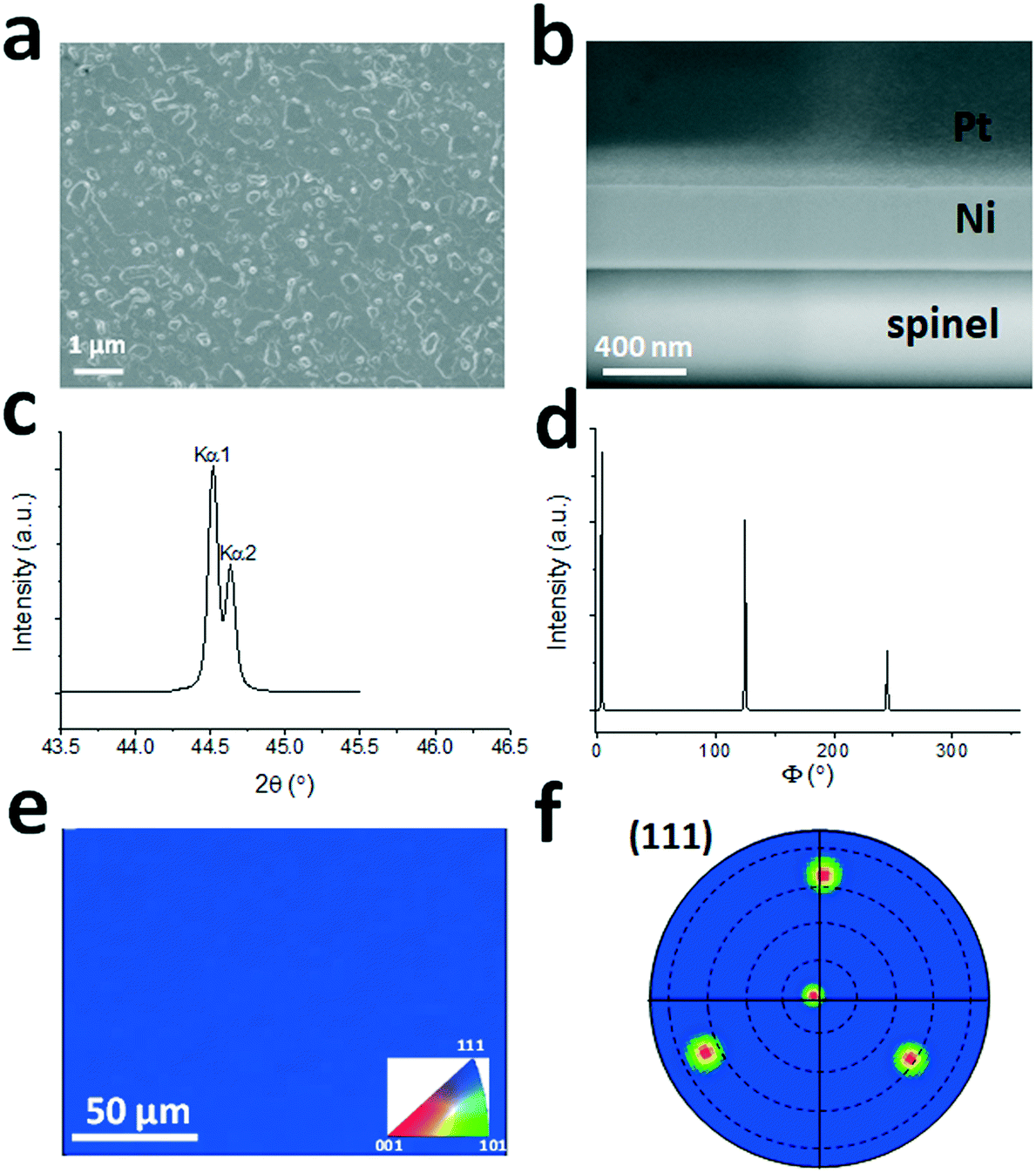 | ||
| Fig. 1 Characterization of single crystalline Ni(111) film deposited on spinel(111) crystal substrate after thermal annealing. (a) SEM image of Ni(111) surface morphology, (b) SEM cross section image of Ni(111) film on spinel(111) substrate prepared by FIB milling, Pt protection film was coated on Ni before FIB milling, (c) high-resolution XRD 2θ–ω scan of the Ni(111) peaks, (d) XRD 360° azimuthal Φ san at χ angle of 70.53° showing Ni(111) peaks, (e) EBSD IPF-X map showing Ni film's in-plane spatial orientation distribution, and (f) EBSD Ni(111) pole figure. | ||
Graphite surface morphology and Raman characterizations
Graphite films were grown on the well characterized single crystalline Ni(111) films at temperatures ranging from 850 to 1075 °C. The growth time was reduced from 90 min at the lowest temperature to 30 min at the highest temperature. Fig. 2(a)–(d) are SEM images showing surface morphology of graphite grown at temperatures of 850, 925, 1000, and 1075 °C, respectively. The scanning area is 360 μm × 240 μm in size. As seen in Fig. 2(a), the graphite grown at 850 °C with a 90 min growth time has a relatively smooth surface, with slightly darker spots scattering across the surface indicating some thicker graphite flakes exist. The longer growth time comparing to those used at higher temperatures was applied to ensure a full coverage of graphite on the Ni(111) surface grown at this temperature. When the temperature is increased to 925 °C (Fig. 2(b)) with a growth time of 60 min, the thicker flakes merge into a large area, smooth film with some lighter color regions indicating thinner graphite. The lower right corner shows a sign of very thick graphite flakes starting to emerge as manifested by the dark color islands at this location. When the temperature is further increased to 1000 °C, very thick graphite flakes start to prevail on the surface, replacing the thinner graphite films, even though the growth time was cut down to 45 min. The thick graphite flakes are mixed with very bright streaks or isles indicating very thin or no graphite formed at these locations (Fig. 2(c)). The inhomogeneous graphite growth results in a rougher surface comparing to the films grown at lower temperatures. When the temperature reaches 1075 °C, although growth time was further reduced to 30 min, the graphite surface becomes very rough (Fig. 2(d)). Thick and small graphite domains are dominant on the surface and alternate with very thin graphite regions in bright color. This kind of surface structure completely replaces the uniformly thin graphite films observed at lower temperatures.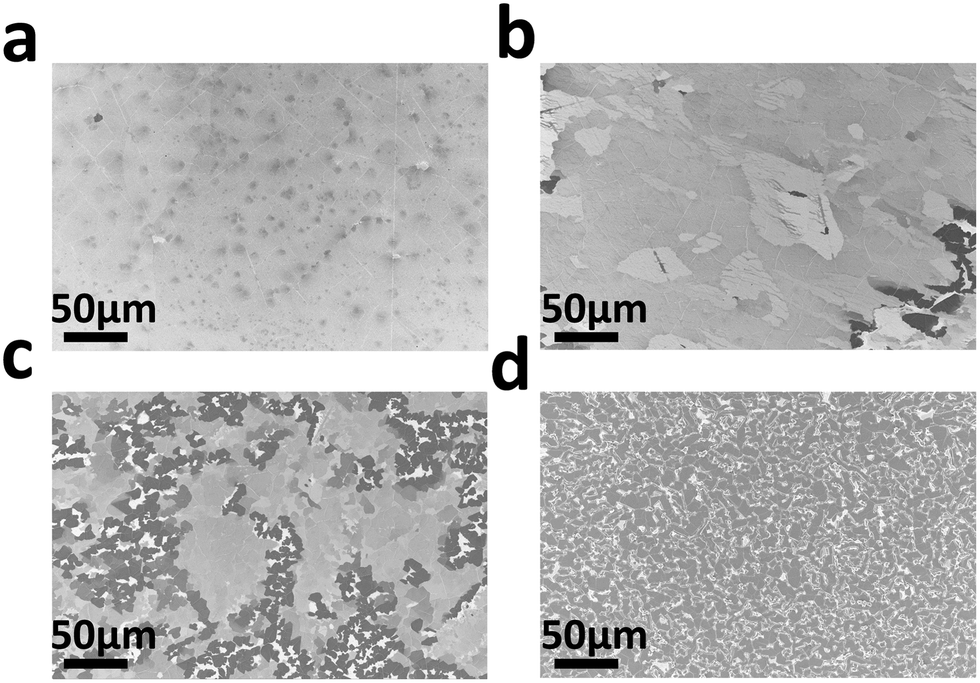 | ||
| Fig. 2 SEM images of graphite films grown on Ni(111) films at different temperatures. (a–d) Graphite films grown at 850, 925, 1000, and 1075 °C, respectively. | ||
The carbon solubility in Ni increases exponentially with the temperature.28 It is expected that, at a higher temperature, a large amount of carbon dissolves into bulk Ni. Thus thick graphite would be formed in the growth process. As mentioned above, for a polycrystalline Ni substrate, in the cooling down stage, the dissolved carbon easily segregated and precipitated onto the surface along the grain boundaries, resulted in an uneven graphite growth. This is the main reason that small scale graphite domains with a large thickness variation form when using a polycrystalline Ni substrate. However, our single crystal Ni is free of grain boundaries, the segregation and precipitation of carbon atoms on the single crystal Ni surface are expected to be evenly distributed and should result in a smooth graphite film. This is relatively true for graphite growth at lower temperatures such as 850 °C and 925 °C. When the temperature increases to above 925 °C, this trend breaks down. It has been reported that, on a polycrystalline Ni substrate, a significant part of Ni can undergo surface restructuring and morphology change. Extra surface steps were observed during the multilayer graphene growth.5 Furthermore, the graphene nucleation and growth impeded Ni steps flow and led to bunching and highly corrugated surface. This caused inhomogeneous carbon diffusion and transport on the Ni surface, and resulted in anisotropic carbon precipitation deviated from the ideal situation. The condition worsened for graphite growth at high temperatures under a long process duration because the highly mobile Ni surface caused a partial graphite coverage even after a long growth period. It appears that this phenomenon is independent of the initial crystal orientation of Ni. It occurs not just on the polycrystalline Ni surface, but on the single crystal Ni substrate as well in our work. The resulting small size, thick graphite flakes unevenly spreading across the Ni surface and the large surface roughness of graphite grown at 1000 °C and 1075 °C shown in Fig. 2(c) and (d) is an indicator demonstrating that the carbon concentration distribution on Ni(111) surface is not homogeneous during the graphite growth at these temperatures.
The obtained graphite films were characterized using Raman spectroscopy. Fig. 3(a) shows four representative Raman spectra of graphite samples. The spectra were taken from smooth graphite regions shown in Fig. 2(a–c) for graphite grown at 850 to 1000 °C. For graphite grown at 1075 °C, Raman spectrum was taken at a random location because the surface is prevailingly rough across the sample. The spectra show that, the G to 2D intensity ratio increases with the temperature, indicating thicker graphite forms at higher temperatures. The peaks at Raman shifts of 1124 cm−1 and 2330 cm−1 are due to instrumental noises. No significant D peak is observed at 1350 cm−1 indicating a good film quality with negligible lattice defects. The G to 2D intensity ratio is consistently larger than 1 and this infers that the graphite layer stacking is likely the AB (Bernal) stacking instead of the turbostratic interlayer rotational stacking, as reported in the literature.11,31 Here the AB stacking is defined as half of the carbon atoms of the graphene layer align normally above half of the carbon atoms of the second layer, while the other half align normally above the centers of the hexagonal lattices of the second layer, which results in interlayer electronic coupling.11,32 On the other hand, the turbostratic stacking refers to a random relative in-plane rotation between the two adjacent graphene layers, which increases the interplanar spacing, and decouples the interlayer interactions.11,33 The 2D peaks also demonstrate an upshift of the wavenumbers with the increase of temperature indicating an increase in the number of layers, which is consistent with the data reported in the literature.34
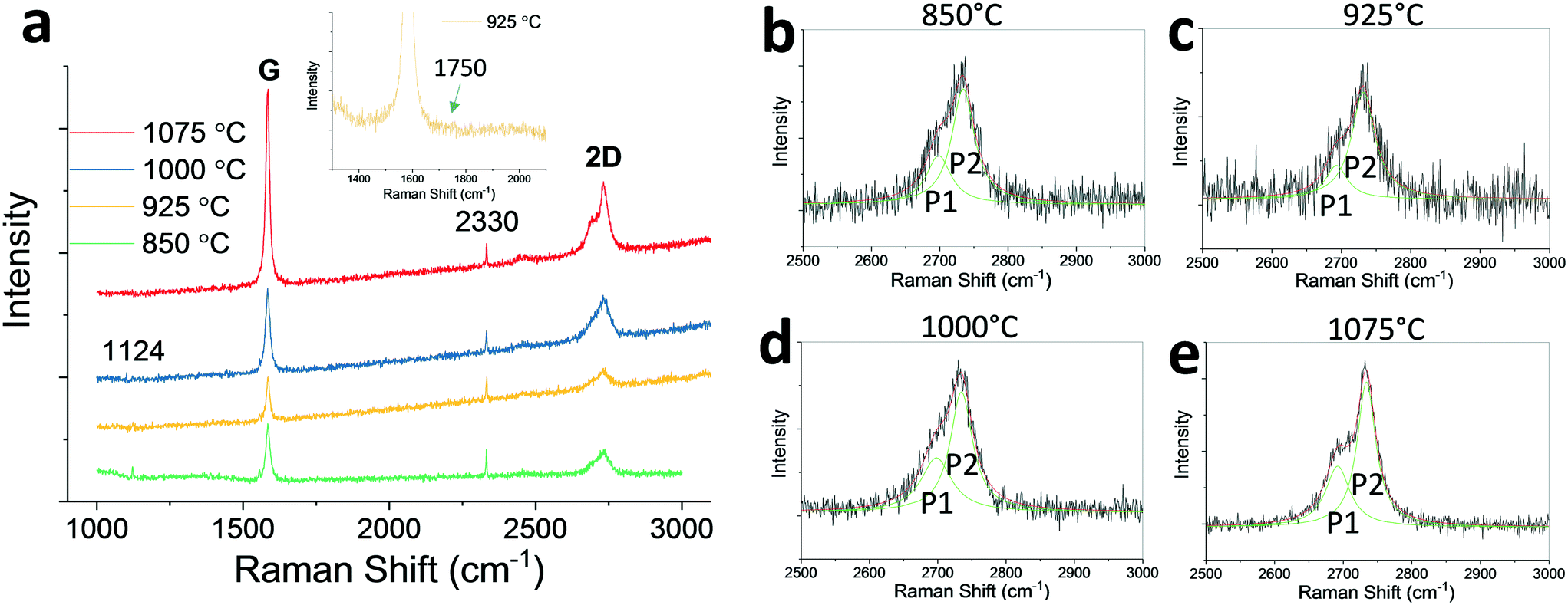 | ||
| Fig. 3 (a) Representative Raman spectra for graphite grown at different temperatures. The inset is a fine scan of Raman spectrum with Raman shift ranges from 1300 to 2100 cm−1 for graphite grown at 925 °C. (b–e) Deconvolution of 2D peaks for graphite grown at temperatures of 850, 925, 1000, and 1075 °C, respectively. | ||
To confirm that the graphite interlayer stacking order is AB stacking, the graphite 2D peaks were further analyzed for graphite films grown at different temperatures. For those spectra, the 2D peaks were deconvoluted into two Lorentzian peaks: P1 and P2. The results are shown in Fig. 3(b–e). As one can see, the low wavenumber P1 peaks located at 2693–2698 cm−1 have relatively lower intensities compared to that of the high wavenumber P2 peaks which are located at 2731–2734 cm−1. The FWHM values for P1 peaks range from 38 to 54 cm−1, and for P2 peaks range from 33 to 40 cm−1. The splitting of the two peaks (2D peak splitting: Δ2D) ranges from 33–41 cm−1. The 2D peak splitting with P2 peak stronger than P1 peak is a further evidence indicating that the graphite film is AB stacking, which is consistent with the data shown in the literature.31 For a graphite film with turbostratic stacking order, due to the interlayer decoupling, the 2D peak typically appears in a single Lorentzian form, similar to the one for a monolayer graphene.31 A fine scan Raman spectrum with Raman shift between 1300 and 2100 cm−1 is shown as inset in Fig. 3(a) for graphite grown at 925 °C before transfer. Furthermore, for graphite with turbostratic stacking order, there exists rotational (R) mode peaks with Raman shift between 1400 and 1500 cm−1, and relatively strong in-plane phonon combination mode peaks between 1800–2100 cm-1.31,35,36 There is no such peaks present in the Raman spectrum shown in Fig. 3(a) inset. To sum up, Raman spectra shown in Fig. 3 confirm that, graphite films grown on Ni(111) have an interlayer AB (Bernal) stacking order with no significant interlayer rotational disorders.
The uniformity of the graphite film grown on Ni(111) was also characterized using Raman area scans on the smooth regions of a sample grown at 925 °C. Raman G, 2D, and G/2D maps were obtained for graphite before transferring to SiO2/Si substrate. The results are shown in Fig. S3.† The Raman G and 2D maps indicate that the graphite film fully covers the Ni substrate for the region scanned. The G/2D map shows consistent G/2D ratio larger than 1, indicating uniform multilayer graphene coverage on the Surface. Furthermore, the G/2D ratio is homogeneously uniform across the whole image. It suggests that the layer number of graphite is unchanged and is uniform for the scanned area. On the other hand, both G and 2D maps show the gradual increase of Raman intensity from bottom to top. This can be caused by the system instability during Raman mapping process, that is, the focus of microscope may drift during the scanning. This can result in the Raman intensity change gradually across the maps. But it does not affect the conclusion drawn above using the Raman G/2D map.
The surface morphology and roughness of graphite films before transferring to other substrates were further characterized using AFM. Three samples grown at 925, 1000, and 1075 °C were examined. The images are shown in Fig. S4.† The scan size is 50 μm × 50 μm. Fig. S4(a)† shows a relatively flat graphite surface grown at 925 °C. The RMS surface roughness is estimated to be 10–13 nm. The grainy look and the steps/terraces on the surface appear coming from the underneath Ni substrate. As shown in Fig. S5,† after the sample undergoes a UV ozone cleaning/removal process (Fig. S5(b)†) to remove the graphite layer, the sample surface (Fig. 5(a)) exhibits a similar topographic look as the one shown in Fig. S4(a)† before the cleaning/removal process. The Raman spectrum shown in Fig. S5(b)† indicates that the graphite film is completely removed from the sample, manifested by the vanishing of both G and 2D peaks. The substantial surface morphology transformation of Ni(111) comparing to the one before graphite growth (shown in Fig. S2†) is consistent with the study in the literature,5 which reported a significant part of Ni can undergo surface restructuring and morphology change, as mentioned above. Fig. S4(b)† shows a AFM image of graphite grown at 1000 °C. A flat region was chosen for the AFM scan. The data shows that the RMS surface roughness increases to 14–15 nm. As mentioned above, when temperature increases to 1075 °C, the very thick graphite domains dominate the sample surface, as shown in Fig. S4(c).† The AFM scan indicates that the surface RMS roughness drastically increases to ∼250 nm.
The graphite thickness is also estimated using AFM height profile analysis by doing line scans across the graphite edge to the bare substrate for graphite samples transferred to SiO2/Si wafers. Fig. S6† shows typical thickness for graphite grown at different temperatures. The thickness is estimated to be 22, 37, 188, and 2554 nm for graphite grown at 850 °C, 925 °C, 1000 °C, and 1075 °C, respectively. Assuming the graphite interlayer spacing is ∼3.35 Å, the estimated graphite layer number is 66, 110, 561, and 7623, respectively.
Graphite EBSD and XRD crystal property characterizations
Because the thickness of graphite films is in the range of tens to hundreds of nanometers, EBSD is considered to be a suitable tool to characterize its structural property. Furthermore, in contrast to transmission electron microscopy and scanning tunneling microscopy which are extensively used to study crystal structure within a localized sample region, EBSD can provide structural information on a much larger area. Thus, EBSD was applied to characterize the graphite films before and after transferring from Ni film to SiO2/Si substrates. The maximum scan size was set at 1.4 mm × 1.1 mm. Here, (10![[1 with combining macron]](https://www.rsc.org/images/entities/char_0031_0304.gif) 1) pole figures are plotted to evaluate the graphite crystallinity. For graphite, the (101) poles have a χ angle of 72.37° relative to the (0001) central pole with a relatively stronger intensity than diffractions from other crystal planes. Because graphite has six-fold symmetry, there will be six (101) poles if it is a single crystal. There will be more than one group of (101) poles if crystalline domains with different orientations exist. Fig. 4(a) shows a (101) pole figure for graphite film grown at 850 °C before the transfer process. The color contour in graphite (101) pole figures indicates the strength of the texture. The red color indicates stronger intensity with more data clustering, and the green color indicates the opposite. In the pole figure, six graphite (101) poles with (0001) out-of-plane orientation are marked by hexagonal shaped orange dash lines. The other 18 stronger (101) poles have χ angles of ∼29°, ∼48°, and ∼85°, respectively. The out-of-plane orientation for these poles is determined to be (11
1) pole figures are plotted to evaluate the graphite crystallinity. For graphite, the (101) poles have a χ angle of 72.37° relative to the (0001) central pole with a relatively stronger intensity than diffractions from other crystal planes. Because graphite has six-fold symmetry, there will be six (101) poles if it is a single crystal. There will be more than one group of (101) poles if crystalline domains with different orientations exist. Fig. 4(a) shows a (101) pole figure for graphite film grown at 850 °C before the transfer process. The color contour in graphite (101) pole figures indicates the strength of the texture. The red color indicates stronger intensity with more data clustering, and the green color indicates the opposite. In the pole figure, six graphite (101) poles with (0001) out-of-plane orientation are marked by hexagonal shaped orange dash lines. The other 18 stronger (101) poles have χ angles of ∼29°, ∼48°, and ∼85°, respectively. The out-of-plane orientation for these poles is determined to be (11![[2 with combining macron]](https://www.rsc.org/images/entities/char_0032_0304.gif) 2) using EBSD inverse pole figure in the Z direction (data not shown). It is believed that these poles are caused by the diffraction from the Ni(111) substrate. For Ni, the lattice constant in the (111) plane is 2.49 Å. The graphite (0001) plane lattice constant is 2.46 Å. The in-plane lattice mismatch is only ∼1.2%.37 If the graphite film is thin enough for electron beam to penetrate through, the EBSD detector can also pick up the diffraction from the substrate. Because EBSD data processor uses graphite lattice parameters to match and index the diffraction patterns, it likely mis-indexes the diffraction from Ni(111) as graphite diffraction, and creates an incorrect out-of-plane graphite orientation. We can see later that these (101) poles related to the out-of-plane (112) orientation disappears in the graphite (101) pole figures after a Ni etching and graphite transfer process. When the temperature increases to above 1000 °C, the graphite (101) poles appear much stronger. At 1075 °C, the graphite (101) poles evolve into two major sets of poles (we will discuss this phenomenon in the next section). The signal from Ni(111) completely disappears when the substrate temperature increases to 1075 °C (data not shown). This is resulted from the significant graphite's thickness increase at high temperatures, which prevents electron beam from reaching the Ni substrate.
2) using EBSD inverse pole figure in the Z direction (data not shown). It is believed that these poles are caused by the diffraction from the Ni(111) substrate. For Ni, the lattice constant in the (111) plane is 2.49 Å. The graphite (0001) plane lattice constant is 2.46 Å. The in-plane lattice mismatch is only ∼1.2%.37 If the graphite film is thin enough for electron beam to penetrate through, the EBSD detector can also pick up the diffraction from the substrate. Because EBSD data processor uses graphite lattice parameters to match and index the diffraction patterns, it likely mis-indexes the diffraction from Ni(111) as graphite diffraction, and creates an incorrect out-of-plane graphite orientation. We can see later that these (101) poles related to the out-of-plane (112) orientation disappears in the graphite (101) pole figures after a Ni etching and graphite transfer process. When the temperature increases to above 1000 °C, the graphite (101) poles appear much stronger. At 1075 °C, the graphite (101) poles evolve into two major sets of poles (we will discuss this phenomenon in the next section). The signal from Ni(111) completely disappears when the substrate temperature increases to 1075 °C (data not shown). This is resulted from the significant graphite's thickness increase at high temperatures, which prevents electron beam from reaching the Ni substrate.
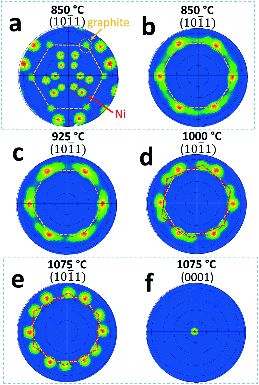 | ||
| Fig. 4 EBSD (101) pole figures with color contour for graphite films grown at different temperatures. (a) Grown at 850 °C. The data show the poles for graphite film on Ni(111) film before transferring to SiO2/Si substrate. The pole figure includes diffraction signal from Ni substrate. The graphite (101) poles are marked with hexagonal shaped orange dash lines. (b)–(e) Grown at 850 °C, 925 °C, 1000 °C, and 1075 °C, respectively, after transferring to 100 nm thick SiO2/Si substrates. Graphite (101) poles from two crystalline domains are marked with hexagonal shaped orange and red dash lines. (f) EBSD (0001) pole figure for graphite film grown at 1075 °C, after transferring to SiO2/Si substrate. | ||
In order to eliminate the interference from Ni film substrate on the graphite crystal structure characterization, Ni was etched away and the graphite films were transferred to SiO2/Si substrates for EBSD scan. Again, the maximum scan size was set at 1.4 mm × 1.1 mm to evaluate the graphite crystallinity. Fig. 4(b)–(e) show EBSD (101) pole figures for graphite films prepared at 850, 925, 1000, and 1075 °C, respectively, after the transfer process. As shown in Fig. 4(b)–(e), the signal from Ni substrates shown in Fig. 4(a) are completely eliminated. For graphite films grown at 850 and 925 °C, there are only one major set of six (101) poles present in the pole figures. However, the in-plane orientation dispersion is relatively large as evident in pole broadening/stretching in azimuthal direction. The average FWHM value of the poles is estimated to be ∼10°. When the temperature increases to 1000 °C and above, a second set of six (101) poles emerges, see Fig. 4(d) and (e). For graphite film grown at 1000 °C, the in-plane angular rotation for the second set of weaker poles is estimated to be 17–20° from the first set of (101) poles, which is not noticeable before the transfer of graphite film due to the interference from the Ni film substrate. For graphite grown at 1075 °C (Fig. 4(e)), the in-plane angular rotation of the second set of poles is estimated to be 22–25°, and the signal of the second set of poles becomes much stronger than the one grown at 1000 °C (Fig. 4(d)). Studies show that, graphene grown on Ni substrate can have multiple domains with 17 ± 7° in-plane rotations at temperatures above 600 °C.20,26,38 Our EBSD data show similar in-plane crystalline domain rotations but it only becomes significant at a temperature much higher than the 600 °C as reported in the literature. Furthermore, for the EBSD scans conducted at a scale of millimeter size, the data show that only one major set of (101) poles exists for graphite grown at lower temperature of 850 (Fig. 4(b)) and 925 °C (Fig. 4(c)). This indicates that the crystalline domain size in the graphite films is at least on the millimeter scale when grown at temperature of 850 and 925 °C. A single crystalline graphite domain of this size has not been reported in the literature. Fig. 4(f) shows the (0001) pole figure for the graphite film grown at 1075 °C, after transferring to 100 nm thick SiO2 buffered Si substrate. The EBSD pole figure confirms that the graphite's out-of-plane orientation is in the [0001] direction.
As a comparison, Fig. S7† shows an EBSD pole figure and a XRD 2θ–ω spectrum of a commercial HOPG sample. The EBSD (101) pole figure in Fig. S7(a)† shows a weak biaxial texture structure present in the HOPG. The XRD data in Fig. S7(b)† show (0002), (0004), and (0006) graphite peaks. This indicates the out-of-plane orientation for the HOPG sample is (0001).
EBSD IPF-Z and IPF-X crystallographic orientation maps are shown in Fig. S8† for graphite grown at 925 °C. The graphite was transferred to a SiO2/Si substrate for EBSD mapping. The scale bar is 200 μm for both maps. The maps show the spatial crystallographic orientation distributions in the out-of-plane Z (Fig. S8(a)†) and in-plane X (Fig. S8(b)†) directions. The insets in both figures are the IPF color legend for the hexagonal crystal system, with the red, green, and blue colors representing the [0001], [110], and [100] directions, respectively. The three colors have certain degrees of spread in the color legend before transitioning into other colors. The angle between the [110], and [100] directions is 30°. As one can see, the IPF-Z map in Fig. S8(a)† indicates the out-of-plane orientation for the graphite film is in the [0001] direction as indicated by the uniform red color. On the other hand, the IPF-X map in Fig. S8(b)† is dominantly green color indicating a prevailing in-plane orientation close to [110] direction. The data further support that, large scale, single crystalline domain exists in the graphite film. The light cyan and light blue colors close to bottom edge of the image indicate that some in-plane misorientation dispersion exists in these locations, which is consistent with the pole figure shown in Fig. 4(c) as the six (101) poles stretching in azimuthal direction.
Because the graphite films are relatively thin for samples grown at a temperature below 1000 °C, it is a challenge to obtain sufficient signal from XRD diffraction. Thus only graphite films grown at 1000 °C and 1075 °C were characterized using XRD. The XRD 360° azimuthal Φ scan results for graphite (101) peaks measured at the chi angle, χ, of 72.37°, are shown in Fig. S9† for graphite film grown at 1000 °C (Fig. S9(a)†) and 1075 °C (Fig. S9(b)†). Note that the XRD spectra were collected from graphite films after transferred to SiO2/Si substrates. Both samples show twelve peaks, indicating that globally two in-plane crystalline domains exist for the two graphite samples measured. The in-plane rotations between the two sets of peaks for samples grown at 1000 °C and 1075 °C are 17–18° and 22–24°, respectively. These values are consistent with the rotation angles observed in EBSD pole figures shown above.
RHEED characterizations of graphite lattice constant and interlayer distance
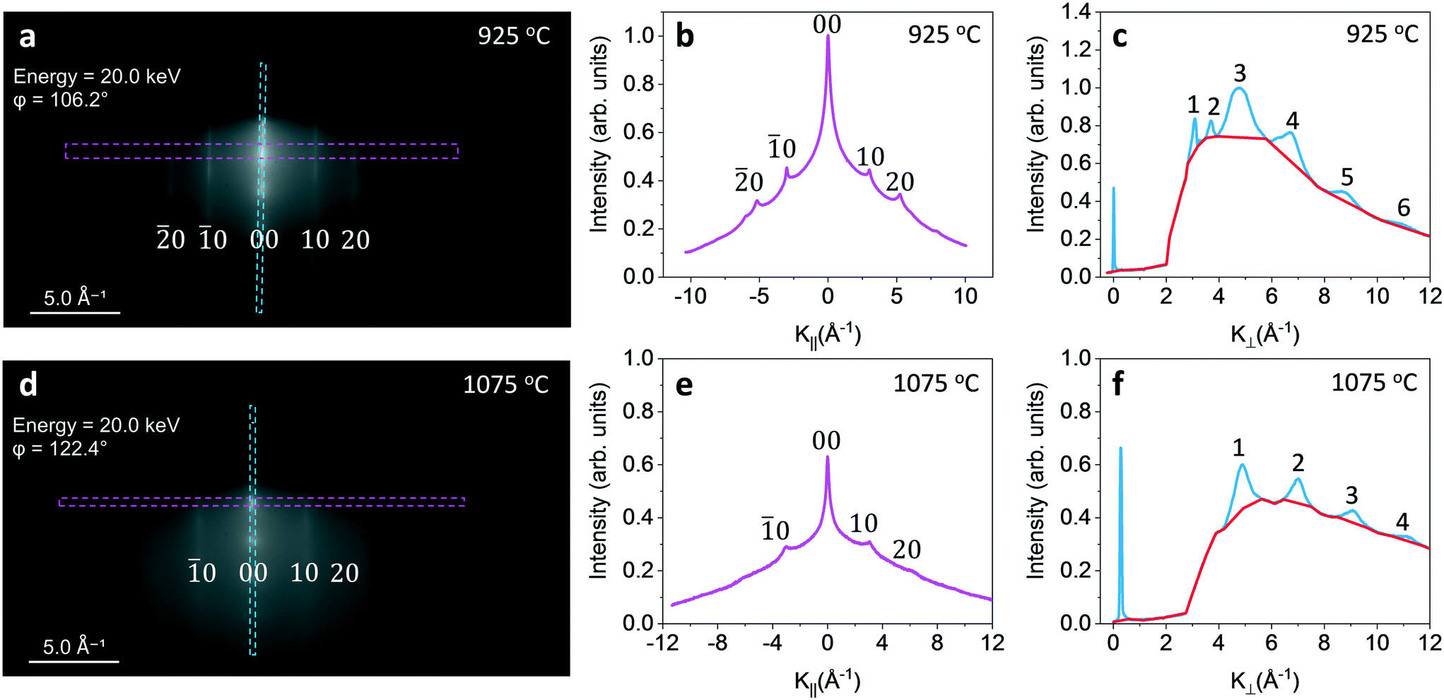
In this section we present the near surface graphite structure quantitatively including in-plane lattice constant and vertical interlayer distance using RHEED. The 20 keV electron used in RHEED has a penetration depth of ∼10 nm and can detect the near surface structure. RHEED patterns from multilayer graphite grown on Ni substrates at 925, 1000 and 1075 °C before being transferred onto SiO2 substrates were collected. Fig. 5(a) shows a RHEED pattern of graphite film grown on Ni substrate at 925 °C. There are spots along the stripes perpendicular to the surface. This is a result of constructive interference between the atomic layers in the graphite film. Fig. 5(b) plots the average intensity parallel to the surface within the magenta dashed rectangle (in Fig. 5(a)) as a function of momentum transfer (k = kout − kin, where kout is the out-going wavevector and kin is the incoming wavevector) parallel to the surface, k||. Peaks are labeled by Miller indices (0), (0), (00), (10), and (20). From the separation Δk|| of adjacent peaks in units of Å−1 one can calculate the lateral lattice constant a = 2π/Δk|| = 2.42 ± 0.02 Å. It is slightly less than bulk graphite lattice unit length of 2.46 Å. Fig. 5(c) plots the average intensity perpendicular to the surface within the blue dashed rectangle as a function of momentum transfer perpendicular to the surface, k⊥. Peaks are labeled by numerical numbers 1 to 6. Peaks 3–6 are from graphite. From the adjacent separation Δk⊥ of graphite peaks the interlayer distance is calculated to be c/2 = 2π/Δk⊥ = 3.08 ± 0.16 Å, less than the bulk interlayer spacing 3.35 Å of graphite. Peak 1 position is consistent with the (111) peak of Ni film substrate. This Ni(111) is consistent with the EBSD pole figure data because the graphite film is thin in some area. The electron beam can penetrate through thin graphite film if its thickness is less than the electron mean free path and can detect Ni. Note the peak intensities of peak 1 and peak 2 from Ni are weaker than peak 3 from graphite. However, their FWHMs are much sharper than that from graphite. This is because the Ni substrate is a better epitaxy film compared to the graphite film. The data for 1000 °C are similar to that of 925 °C and are not shown here. Fig. 5(d)–(f) are similar data for the graphite film grown on Ni at 1075 °C except that the first two peaks 1 and 2 in Fig. 5(c) disappear. This is also consistent with no Ni poles in the EBSD data at 1075 °C. Recall the graphite film grown at 1075 °C is much thicker than the penetration depth ∼10 nm of 20 keV electrons used in the RHEED.
 | ||
| Fig. 5 (a) RHEED pattern, (b) intensity vs. momentum transfer parallel to the surface k|| and (c) intensity vs. momentum transfer perpendicular to the surface k⊥ for graphite film grown on Ni(111) film at 925 °C. Similarly, (d)–(f) are for graphite film grown on Ni(111) at 1075 °C. The red curves in (c) and (f) are RHEED background intensities. | ||
Geometrical superlattice area mismatch model (GSAM) for graphite and Ni epitaxial relationship estimation
A GSAM model is applied to evaluate the epitaxial relationship between graphite and Ni lattices using single layer graphene as an example. As described in the literature,39–42 the model examines the pairs of superlattices formed at the interface of epitaxial overlayer and the substrate. It identifies close coincidence lattices with minimal lattice area mismatch for the two materials. The superlattice minimizes the energy of the epitaxy system with high superlattice matching density, and thus is preferred during the epitaxial growth. The model is defined as: ΔA = A[(Δu/u) + (Δv/v) + (Δθ/tanθ)]. Here ΔA is the area mismatch between the overlayer superlattice and substrate superlattice. A, u, v, and θ, represent the area of superlattice, the two superlattice unit vectors, and the angle between overlayer and substrate superlattices unit vectors, respectively. In this calculation, the maximums of A, Δu/u, Δv/v, and Δθ/tanθ are set to be 400 Å2, 5%, 5%, and 5%, respectively. The rotation angle is defined as the angle between unit vectors ![[a with combining right harpoon above (vector)]](https://www.rsc.org/images/entities/i_char_0061_20d1.gif) graphene and Ni(111). The lattice constants used for the calculation are graphene (0001), a = b = 2.46 Å, α = 60°; and Ni (111), a = b = 2.49 Å, α = 60°. Fig. 6(a) shows the calculated results for graphene/Ni system. The radius of the circles in Fig. 6(a) is scaled inversely proportional to A. Here we can identify that the smallest ΔA (0.15 Å2) happens to be the data point at the rotation angle of 0° with the largest circle, corresponding to the most favorable alignment between graphene and Ni(111). In this case, graphene is aligned parallel to the Ni(111) surface during the epitaxial growth, with graphene(0001)∥Ni(111) and
graphene and Ni(111). The lattice constants used for the calculation are graphene (0001), a = b = 2.46 Å, α = 60°; and Ni (111), a = b = 2.49 Å, α = 60°. Fig. 6(a) shows the calculated results for graphene/Ni system. The radius of the circles in Fig. 6(a) is scaled inversely proportional to A. Here we can identify that the smallest ΔA (0.15 Å2) happens to be the data point at the rotation angle of 0° with the largest circle, corresponding to the most favorable alignment between graphene and Ni(111). In this case, graphene is aligned parallel to the Ni(111) surface during the epitaxial growth, with graphene(0001)∥Ni(111) and ![[b with combining right harpoon above (vector)]](https://www.rsc.org/images/entities/i_char_0062_20d1.gif) graphene(0001)∥Ni(111). On the other hand, there are other possible epitaxial relationships that exist in the system with different relative in-plane lattice rotations. The rotation configurations shown in the experimental results are labeled with red circles. As one can see, the graphene domain with an in-plane 17° rotation angle, relative to the Ni(111) lattice, which is observed in the experiments, has a higher superlattice area mismatch value of 2.2 Å2, indicating relatively higher system energy in this epitaxial configuration. There are other two graphene domains relatively close to each other with rotation angles of 22° and 25° relative to the Ni(111) lattice, showing smaller ΔA of 0.6 Å2 and 0.9 Å2, respectively, with lower system energy. These domains are also observed in the experimental results of EBSD shown above, especially in the graphite samples grown at highest temperatures of 1000 °C and 1075 °C. Fig. 6(b) shows 2D real space lattice overlays for graphite (0001) epitaxy on Ni(111). The graphite lattices with four in-plane rotation angles (0°, 17°, 22°, and 25°) observed in the experiments are drawn to demonstrate the epitaxial relationship. When graphite and Ni lattices are at 0° in-plane relative rotation, the lattice mismatch is only ∼1%, that results in coincidence for all the lattice points. At other rotation angles, the superlattices of graphite and Ni are much larger, and most of the lattice points will not coincide, which results in higher energy in the system, and lower possibility of occurrence. Because of the large in-plane misorientation dispersions in the experimental data, it is difficult to identify which rotation angle has the exact match to the experimental results. Nevertheless, the GSAM model calculation results are consistent with our observed experimental data regarding to the graphite crystalline domain rotation angles.
graphene(0001)∥Ni(111). On the other hand, there are other possible epitaxial relationships that exist in the system with different relative in-plane lattice rotations. The rotation configurations shown in the experimental results are labeled with red circles. As one can see, the graphene domain with an in-plane 17° rotation angle, relative to the Ni(111) lattice, which is observed in the experiments, has a higher superlattice area mismatch value of 2.2 Å2, indicating relatively higher system energy in this epitaxial configuration. There are other two graphene domains relatively close to each other with rotation angles of 22° and 25° relative to the Ni(111) lattice, showing smaller ΔA of 0.6 Å2 and 0.9 Å2, respectively, with lower system energy. These domains are also observed in the experimental results of EBSD shown above, especially in the graphite samples grown at highest temperatures of 1000 °C and 1075 °C. Fig. 6(b) shows 2D real space lattice overlays for graphite (0001) epitaxy on Ni(111). The graphite lattices with four in-plane rotation angles (0°, 17°, 22°, and 25°) observed in the experiments are drawn to demonstrate the epitaxial relationship. When graphite and Ni lattices are at 0° in-plane relative rotation, the lattice mismatch is only ∼1%, that results in coincidence for all the lattice points. At other rotation angles, the superlattices of graphite and Ni are much larger, and most of the lattice points will not coincide, which results in higher energy in the system, and lower possibility of occurrence. Because of the large in-plane misorientation dispersions in the experimental data, it is difficult to identify which rotation angle has the exact match to the experimental results. Nevertheless, the GSAM model calculation results are consistent with our observed experimental data regarding to the graphite crystalline domain rotation angles.
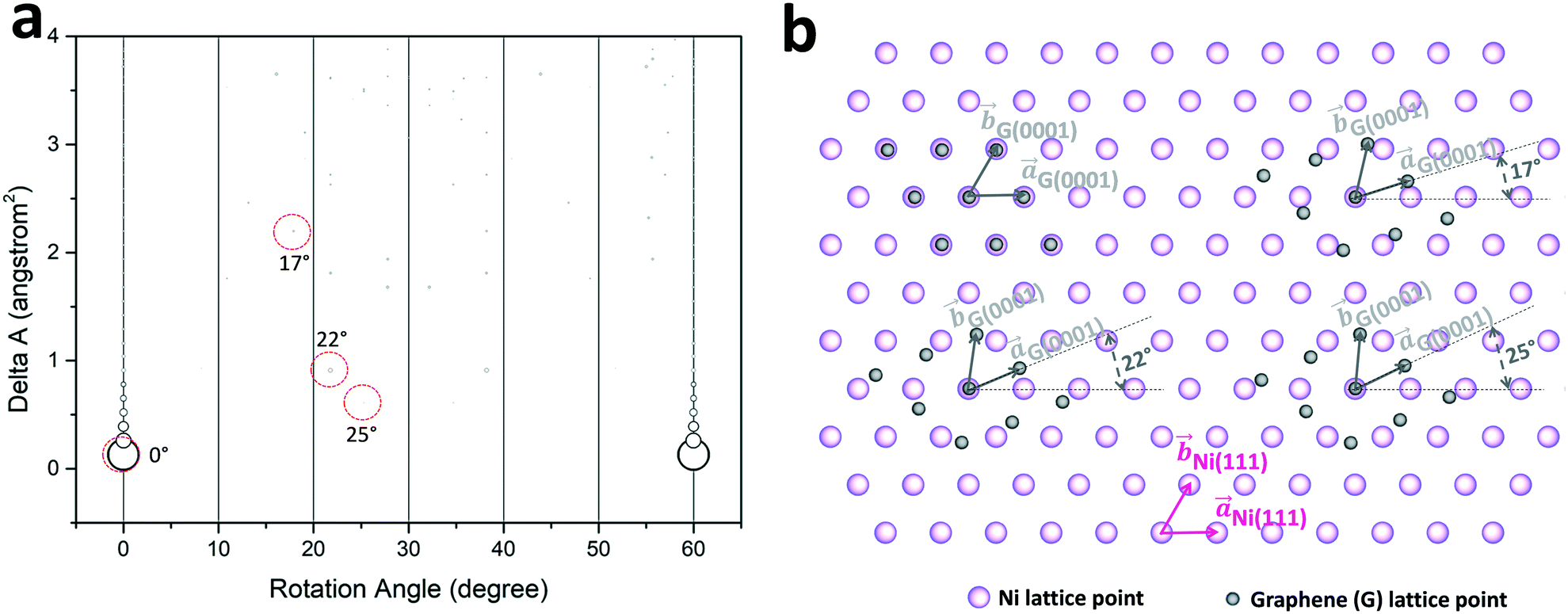 | ||
| Fig. 6 (a) Plot of the superlattice area mismatch (delta A) of epitaxial relationship between graphene and Ni(111) substrate. The data appeared in the experimental results are labeled by red circles. (b) Schematic of 2D real space lattice overlays for graphite (0001) on Ni(111) with rotation angles of 0°, 17°, 22°, and 25°. Graphite crystalline domain with rotation angle of 0° is the most favorable configuration with the smallest delta A value. | ||
Conclusion
In summary, using AFM, SEM-FIB, Raman spectroscopy, EBSD, XRD and RHEED techniques, we studied surface morphology and crystal properties of graphite films grown on single crystalline Ni(111). The data indicate that the graphite film is grown on Ni with AB (Bernal) stacking at temperature ranging from 850 to 1075 °C. Similar to multilayer graphene grown on polycrystalline Ni substrate, our data indicate significant Ni surface morphology change and restructuring during the graphite growth on the single crystalline substrate. High mobility of Ni atoms combined with graphene nucleation and growth possibly cause inhomogeneous distribution of carbon concentration and result in uneven growth of graphite film especially at temperatures above 925 °C, which significantly roughens the graphite surfaces. On the other hand, the crystal property characterization on these graphite films indicate that, at temperatures ranging from 850 to 925 °C, a single crystalline domain is formed in the graphite film with a size of a millimeter or larger. When the substrate temperature increases to above 925 °C, a second crystalline domain starts to emerge. When the temperature reaches 1075 °C, two crystalline domains co-exist in the graphite films with a relative in-plane orientation rotation of ∼22–25°. Smaller crystalline domain forms with size ranges from tens to a hundred of micrometers at this temperature.Conflicts of interest
There are no conflicts to declare.Acknowledgements
This work is supported by the NYSTAR Focus Center at RPI, C150117. The authors would like to thank the Micro and Nano Fabrication Clean Room (MNCR) staff at RPI for facilitating the experimental work. The authors would also like to thank Prof. Nikhil Koratkar for graphene CVD furnace usage.References
- E. L. Evans, O. P. Bahl and J. M. Thomas, Carbon, 1967, 5, 587–589 CrossRef CAS
.
- M. D. Chinn and S. C. Fain, Phys. Rev. Lett., 1977, 39, 146–149 CrossRef CAS
-
J. G. Dash, Films on Solid Surfaces The Physics and Chemistry of Physical Adsorption, Elsevier Science, Saint Louis, 1st edn, 1975 Search PubMed
- S. Latil and L. Henrard, Phys. Rev. Lett., 2006, 97, 036803 Search PubMed
- J. Kozlova, A. Niilisk, H. Alles and V. Sammelselg, Carbon, 2015, 94, 160–173 CrossRef CAS
- H. Q. Ta, D. J. Perello, D. L. Duong, G. H. Han, S. Gorantla, V. L. Nguyen, A. Bachmatiuk, S. V. Rotkin, Y. H. Lee and M. H. Rümmeli, Nano Lett., 2016, 16, 6403–6410 CrossRef CAS PubMed
- E. V. Castro, K. S. Novoselov, S. V. Morozov, N. M. R. Peres, J. M. B. L. dos Santos, J. Nilsson, F. Guinea, A. K. Geim and A. H. C. Neto, Phys. Rev. Lett., 2007, 99, 216802 CrossRef PubMed
- Z. Ni, L. Liu, Y. Wang, Z. Zheng, L.-J. Li, T. Yu and Z. Shen, Phys. Rev. B: Condens. Matter Mater. Phys., 2009, 80, 125404 CrossRef
- R. W. Havener, H. Zhuang, L. Brown, R. G. Hennig and J. Park, Nano Lett., 2012, 12, 3162–3167 CrossRef CAS PubMed
- X. Zhang, W.-P. Han, X.-F. Qiao, Q.-H. Tan, Y.-F. Wang, J. Zhang and P.-H. Tan, Carbon, 2016, 99, 118–122 CrossRef CAS
- J. A. Garlow, L. K. Barrett, L. Wu, K. Kisslinger, Y. Zhu and J. F. Pulecio, Sci. Rep., 2016, 6, 19804 CrossRef CAS
- S. S. Datta, D. R. Strachan, E. J. Mele and A. T. C. Johnson, Nano Lett., 2009, 9, 7–11 CrossRef CAS PubMed
- Z. Luo, L. A. Somers, Y. Dan, T. Ly, N. J. Kybert, E. J. Mele and A. T. C. Johnson, Nano Lett., 2010, 10, 777–781 CrossRef CAS
- H. Zhou, C. Qiu, Z. Liu, H. Yang, L. Hu, J. Liu, H. Yang, C. Gu and L. Sun, J. Am. Chem. Soc., 2010, 132, 944–946 CrossRef CAS PubMed
- A. S. Ahmed, H. Wen, T. Ohta, I. V. Pinchuk, T. Zhu, T. Beechem and R. K. Kawakami, J. Cryst. Growth, 2016, 447, 5–12 CrossRef CAS
- M. M. Ugeda, A. J. Bradley, S.-F. Shi, F. H. da Jornada, Y. Zhang, D. Y. Qiu, W. Ruan, S.-K. Mo, Z. Hussain, Z.-X. Shen, F. Wang, S. G. Louie and M. F. Crommie, Nat. Mater., 2014, 13, 1091–1095 CrossRef CAS
- L. G. De Arco, Y. Zhang, A. Kumar and C. Zhou, IEEE Trans. Nanotechnol., 2009, 8, 135–138 Search PubMed
- Y. Zhang, L. Gomez, F. N. Ishikawa, A. Madaria, K. Ryu, C. Wang, A. Badmaev and C. Zhou, J. Phys. Chem. Lett., 2010, 1, 3101–3107 CrossRef CAS
- J. C. Shelton, H. R. Patil and J. M. Blakely, Surf. Sci., 1974, 43, 493–520 CrossRef CAS
- Z. Fogarassy, M. H. Rümmeli, S. Gorantla, A. Bachmatiuk, G. Dobrik, K. Kamarás, L. P. Biró, K. Havancsák and J. L. Lábár, Appl. Surf. Sci., 2014, 314, 490–499 CrossRef CAS
- S. Vishwanath, X. Liu, S. Rouvimov, P. C. Mende, A. Azcatl, S. McDonnell, R. M. Wallace, R. M. Feenstra, J. K. Furdyna, D. Jena and H. Grace Xing, 2D Mater., 2015, 2, 024007 CrossRef
- S. C. Stuart, E. Satchet, A. Sandin, J.-P. Maria, J. E. Rowe, D. B. Dougherty and M. Ulrich, J. Vac. Sci. Technol., B: Nanotechnol. Microelectron.: Mater., Process., Meas., Phenom., 2013, 31, 051804 Search PubMed
- T. Iwasaki, H. J. Park, M. Konuma, D. S. Lee, J. H. Smet and U. Starke, Nano Lett., 2011, 11, 79–84 CrossRef CAS
- M. Xu, D. Fujita, K. Sagisaka, E. Watanabe and N. Hanagata, ACS Nano, 2011, 5, 1522–1528 CrossRef CAS
- R. Addou, A. Dahal, P. Sutter and M. Batzill, Appl. Phys. Lett., 2012, 100, 021601 CrossRef
- L. L. Patera, C. Africh, R. S. Weatherup, R. Blume, S. Bhardwaj, C. Castellarin-Cudia, A. Knop-Gericke, R. Schloegl, G. Comelli, S. Hofmann and C. Cepek, ACS Nano, 2013, 7, 7901–7912 CrossRef CAS PubMed
- R. Rameshan, V. Vonk, D. Franz, J. Drnec, S. Penner, A. Garhofer, F. Mittendorfer, A. Stierle and B. Klötzer, Sci. Rep., 2018, 8, 2662 CrossRef
- L. Baraton, Z. B. He, C. S. Lee, C. S. Cojocaru, M. Châtelet, J.-L. Maurice, Y. H. Lee and D. Pribat, EPL, 2011, 96, 46003 CrossRef
- F. Tang, T. Parker, G.-C. Wang and T.-M. Lu, J. Phys. D: Appl. Phys., 2007, 40, R427–R439 CrossRef CAS
- Y. Xiang, F.-W. Guo, T.-M. Lu and G.-C. Wang, Nanotechnology, 2016, 27, 485703 CrossRef CAS PubMed
- A. Niilisk, J. Kozlova, H. Alles, J. Aarik and V. Sammelselg, Carbon, 2016, 98, 658–665 CrossRef CAS
- J. D. Bernal, Proc. R. Soc. A, 1924, 106, 749–773 CrossRef CAS
- Y. Shibuta and J. A. Elliott, Chem. Phys. Lett., 2011, 512, 146–150 CrossRef CAS
- A. C. Ferrari, J. C. Meyer, V. Scardaci, C. Casiraghi, M. Lazzeri, F. Mauri, S. Piscanec, D. Jiang, K. S. Novoselov, S. Roth and A. K. Geim, Phys. Rev. Lett., 2006, 97, 187401 CrossRef CAS
- R. Rao, R. Podila, R. Tsuchikawa, J. Katoch, D. Tishler, A. M. Rao and M. Ishigami, ACS Nano, 2011, 5, 1594–1599 CrossRef CAS
- C. Cong, T. Yu, R. Saito, G. F. Dresselhaus and M. S. Dresselhaus, ACS Nano, 2011, 5, 1600–1605 CrossRef CAS
- D. W. Kim, S. J. Kim, H. O. Choi and H.-T. Jung, Adv. Mater. Interfaces, 2016, 3, 1500741 CrossRef
- A. Dahal, R. Addou, P. Sutter and M. Batzill, Appl. Phys. Lett., 2012, 100, 241602 CrossRef
- A. Zur and T. C. McGill, J. Appl. Phys., 1984, 55, 378–386 CrossRef CAS
- A. S. Yapsir, C.-H. Choi and T.-M. Lu, J. Appl. Phys., 1990, 67, 796–799 CrossRef CAS
- X. Sun, Z. Lu, W. Xie, Y. Wang, J. Shi, S. Zhang, M. A. Washington and T.-M. Lu, Appl. Phys. Lett., 2017, 110, 153104 CrossRef
- Z. Lu, X. Sun, M. A. Washington and T.-M. Lu, J. Phys. D: Appl. Phys., 2018, 51, 095301 CrossRef
Footnote |
| † Electronic supplementary information (ESI) available. See DOI: 10.1039/c9ce01515a |
| This journal is © The Royal Society of Chemistry 2020 |