
A systematic study of MOCVD reactor conditions and Ga memory effect on properties of thick InAl(Ga)N layers: a complete depth-resolved investigation
Prerna
Chauhan
 *a,
S.
Hasenöhrl
a,
Ľ.
Vančo
b,
P.
Šiffalovič
c,
E.
Dobročka
a,
D.
Machajdík
ad,
A.
Rosová
a,
F.
Gucmann
e,
J.
Kováč
Jr
f,
I.
Maťko
c,
M.
Kuball
e and
J.
Kuzmík
a
*a,
S.
Hasenöhrl
a,
Ľ.
Vančo
b,
P.
Šiffalovič
c,
E.
Dobročka
a,
D.
Machajdík
ad,
A.
Rosová
a,
F.
Gucmann
e,
J.
Kováč
Jr
f,
I.
Maťko
c,
M.
Kuball
e and
J.
Kuzmík
a
aInstitute of Electrical Engineering, Slovak Academy of Sciences, Bratislava, Slovakia. E-mail: prerna.chauhan@savba.sk
bSlovak University of Technology, Univ. Sci. Park Bratislava Centre, Vazovova 5, 812 43 Bratislava, Slovakia
cInstitute of Physics, Slovak Academy of Sciences, Bratislava, Slovakia
dJoint Institute for Nuclear Research, Dubna, Russia
eCenter for Device Thermography and Reliability, University of Bristol, Bristol BS8 1TL, UK
fInternational Laser Centre, Ilkovičova 3, Bratislava, Slovakia
First published on 26th November 2019
Abstract
Thick InAlN layers (In-molar fraction >0.37) on GaN buffer layers were prepared using a close-coupled showerhead metalorganic chemical vapor deposition (MOCVD) reactor. This work provides a discussion of the dependence of reactor parameters (pressure, ammonia flow and temperature) and unintentional Ga-incorporation on structural, optical and chemical properties of those layers down to the nanoscale. Rutherford back-scattering spectrometry, Auger electron spectroscopy, and transmission electron microscopy with the energy dispersive X-ray analysis were used for in-depth chemical analysis of layers. A diminishing Ga-auto-incorporation in thick InAlN layer creates a chemically graded InAl(Ga)N interlayer that assists in releasing of interfacial strain and paves the way toward In-rich InAlN layer. The rate of unintentional Ga-auto-incorporation in InAlN layers increases with decreasing of growth temperature, and increasing of reactor pressure and ammonia flow during growth. Raman and photoluminescence spectroscopy were used to get the crystal structural fingerprint influenced by Ga-incorporation. We suggested that Ga could incorporate at nitrogen vacancies at high reactor pressures (≥200 mbar). Screw dislocations and/or N-vacancies in InAl(Ga)N layers may be energetically favorable sites for In-incorporation and lead to compositional fluctuation and local In-rich InAl(Ga)N phase.
Introduction
The InAlN semiconductor with its direct bandgap tunable from 0.65 to 6.2 eV is in a great demand from the application viewpoint in optical and electronic devices. Among them, the most recent one is the use of In-rich InAlN as a buffer layer for InN-channel high electron mobility transistors (HEMTs).1,2 Because of the matured metalorganic chemical vapor deposition (MOCVD) growth technology of resistive GaN buffer, a successive growth of thick InAlN on GaN buffer layer is an obvious choice as per heterostructure (HS) fabrication requirements. The MOCVD growth InAlN on GaN leads to the unintentional incorporation of Ga into InAlN layer and the resultant layer would be InAl(Ga)N quaternary alloy.1–5 Depending on the growth conditions, the origin of Ga could be either reactor environment due to the memory effect of a previous GaN buffer layer1,3–5 or out-diffusion from GaN buffer (GaN decomposition under hydrogen).2MOCVD growth of In-rich InAlN is very challenging due to the very different optimal growth conditions of binaries InN, GaN and AlN. Reuters et al.3 have also proposed a virtual multi-layer model to describe relaxation and In-incorporation in thin (52–75 nm) InAl(Ga)N layers in the direction of growth by means of Rutherford backscattering spectrometry (RBS) and high-resolution X-ray diffraction (HR-XRD). Precise control of the elemental molar fraction and their in-depth distribution is crucial to ensure desired optical and electronic properties of InAlN layers.
In our previous work,1 we demonstrated that diminishing Ga depth profile in InAl(Ga)N layer growth is helping in strain relaxation, which further assists in In-incorporation. We observed that under N2 carrier gas, the unintentionally incorporated Ga create an InAl(Ga)N layer at the interface with GaN buffer. In subsequent layer growth, a graded InAl(Ga)N layer accompanied by strain relaxation to reach InAlN with Ga ∼ 0 was formed. A crucial parameter for InAl(Ga)N growth is ammonia (NH3) flow to supply sufficient N content to avoid features formed in InAl(Ga)N due to N deficiency, like pits with N vacancies and In droplets. NH3 decomposition efficiency is low at growth temperature ∼700 °C, so high partial pressure of NH3 is highly recommended. In MOCVD, the high partial pressure of any element can be achieved by either high reactor pressure or high flow. High reactor pressure promotes the reaction between trimethylaluminum (TMAl) and NH3 that leads to the enhanced adducts formation.9,10 Consequently, less Al-containing moieties would be available for taking part in InAl(Ga)N layer formation on the substrate surface and all together limit the growth rate. The high NH3 partial pressure generates a high amount of H2 molecules, which reduces In droplets on InAl(Ga)N surface but at the same time reduces In-incorporation and enhances pit density. Similar observations were reported earlier.9–11
In the present work, the influence of growth parameters on depth-profile of Ga-auto-incorporation is discussed in detail. Up to now, defects evolution and characteristics of dislocations associated with InAlN layers have been investigated microscopically by transmission electron microscopy (TEM).6–8 However, for InAl(Ga)N layers such investigations are still missing and we contribute to fill this gap. To validate the In-molar fraction and Ga-auto-incorporation due to the memory effect, the samples were analyzed by RBS, Auger electron spectroscopy (AES) and TEM with the energy dispersive X-ray (EDX) analysis that provide complementary insights by probing the chemical composition depth-profile, layer quality and defects along the growth direction.
Experiment
A series of samples was grown with H2 carrier gas, details can be found in our previous publication.1 They were used to study the influence of the decreasing growth temperature from 790 to 730 °C on elemental composition. Another series of InAlN layers was grown with N2 carrier gas by MOCVD in the reactor pressure range of 70 (ref. 1) to 400 mbar and NH3 flow from 1500 (ref. 1) to 4500 sccm at a constant temperature of 730 °C. Electronic grade (99.999%) trimethylgallium (TMGa), trimethylaluminum (TMAl) and trimethylindium (TMIn) were used as precursors for Ga, Al and In, respectively. High purity NH3 (grade N7.0 = 99.99999%) was used as source of nitrogen. Table 1 summarizes details of samples. In all these samples, InAlN layer was grown in sequence with GaN buffer layer. Consequently, an unintentional Ga-auto-incorporation is expected in InAlN layers1 and in the following text, we will use the chemical formula InAl(Ga)N instead of InAlN.![[1 with combining macron]](https://www.rsc.org/images/entities/char_0031_0304.gif) 1 ω scans, and RMS surface roughness
1 ω scans, and RMS surface roughness
| Samples | T (°C) | Carrier gas | P (mbar) | Q vol NH3 (sccm) | V/III ratio | t (nm) | In m.f. XRD | InAl(Ga)N | AFM RMS (nm) | |
|---|---|---|---|---|---|---|---|---|---|---|
| ω 0002 (°) FWHM |
ω 101 (°) FWHM |
|||||||||
| S1 (ref. 1) | 790 | H2 | 70 | 1500 | 5087 | 165 | 0.09/0.12 | 0.20 | 0.60 | 3.1 |
| S2 (ref. 1) | 775 | H2 | 70 | 1500 | 5087 | 171 | 0.11/0.13 | 0.22 | 0.62 | 8.9 |
| S3 (ref. 1) | 760 | H2 | 70 | 1500 | 5087 | 210 | 0.15 | 0.17 | 0.32 | 9.5 |
| S4 (ref. 1) | 730 | H2 | 70 | 1500 | 5087 | 220 | 0.18 | 0.12 | 0.40 | 30.6 |
| S5 (ref. 1) | 730 | N2 | 70 | 1500 | 5087 | 285 | 0.37 | 0.66 | 1.6 | 3.8 |
| S6 | 730 | N2 | 70 | 2000 | 6783 | 300 | 0.36 | 0.51 | 1.4 | 9.5 |
| S7 | 730 | N2 | 70 | 2500 | 8478 | 296 | 0.35 | 0.53 | 1.2 | 8 |
| S8 | 730 | N2 | 70 | 3000 | 10![[thin space (1/6-em)]](https://www.rsc.org/images/entities/char_2009.gif) 174 174 |
300 | 0.36 | 0.54 | 1.2 | 6 |
| S9 | 730 | N2 | 100 | 1500 | 5087 | 260 | 0.37 | 0.77 | 1.4 | 4.3 |
| S10 | 730 | N2 | 150 | 1500 | 5087 | 316 | 0.37 | 0.54 | 1.4 | 6.8 |
| S11 | 730 | N2 | 200 | 1500 | 5087 | 283 | 0.38 | 0.73 | 1.8 | 8 |
| S12 | 730 | N2 | 200 | 3000 | 10174 |
274 | 0.41 | 0.83 | 1.4 | 10.5 |
| S13 | 730 | N2 | 200 | 4500 | 15261 |
235 | 0.38 | 0.83 | 1.5 | 16 |
| S14 | 730 | N2 | 250 | 3000 | 10174 |
215 | 0.41 | 0.76 | 1.4 | 15 |
| S15 | 730 | N2 | 250 | 4500 | 15261 |
117 | 0.40 | 0.70 | 1.4 | 10 |
| S16 | 730 | N2 | 300 | 3000 | 10174 |
224 | 0.42 | 0.73 | 1.5 | 27.5 |
| S17 | 730 | N2 | 300 | 4500 | 15261 |
160 | 0.43 | 0.52 | 1.5 | 30.7 |
| S18 | 730 | N2 | 350 | 3000 | 10174 |
178 | 0.44 | 0.53 | 1.8 | 13 |
| S19 | 730 | N2 | 400 | 3000 | 10174 |
111 | 0.47 | 0.36 | 1.5 | 16.8 |
| S20 | 730 | N2 | 400 | 3500 | 11869 |
120 | 0.46 | 0.38 | 1.3 | 21.7 |
| S21 (ref. 13) | 730 | N2 | 400 | 4500 | 15261 |
112 | 0.47 | 0.49 | 1.1 | 7.8 |
For all samples, XRD 2θ/ω 0002 and 101 scans were carried out on Bruker D8 DISCOVER diffractometer to evaluate the crystalline quality and approximate In-molar fraction.12 Atomic force microscopy (AFM) (NTEGRA Prima, in tapping-mode) and scanning electron microscope (SEM) (FEI Quanta 250 FEG) were used to characterize the surface morphology. LayTec EpiCurve® TT in situ monitoring system was used to extract growth rate (Rg) and the thickness (t) of InAl(Ga)N layers with pyrometer reflectance at 632.7 nm. Cross-sectional SEM was used to verify the thickness of InAl(Ga)N layers with an approximate 5% error as estimated by in situ reflectance curves. Absorption (UV-VIS-NIR Spectrophotometer SolidSpec-3700) and photoluminescence (PL, OLYMPUS BX51 microscope with He-Cd laser 325 nm) measurements were done to characterize the InAl(Ga)N layers grown under different conditions. For Raman spectroscopy, Renishaw InVia™ spectrometer in backscattering geometry was used with a 488 nm excitation laser wavelength. To check the In-molar fraction and Ga-auto-incorporation due to the memory effect, selected samples were investigated by Auger depth profiling (JEOL JAMP 9510-F Auger microprobe, using 10 keV electron excitation with 10 nA beam current, 55° tilt with respect to primary electron beam, normal take-off angle), Rutherford backscattering spectrometry (RBS) and high-resolution transmission electron microscopy (HRTEM). Polarity was determined by using convergent beam electron diffraction (CBED) patterns along the [100] zone axis of GaN buffer, as we did not detect any inversion domain at the InAl(Ga)N/GaN interface, we can state that the samples investigated here are In-polar grown on Ga-polar GaN buffer layer. High-angle annular dark-field (HAADF) and bright-field (BF) images were taken to evaluate the chemical contrast together with EDX analysis using an aberration-corrected FEI Titan Themis 300 microscope in STEM mode. The microscope was operated at 200 kV acceleration voltage and EDX acquisition was carried out using a Super-X detector system (ChemiSTEM technology).
Results
A. Role of the reactor pressure
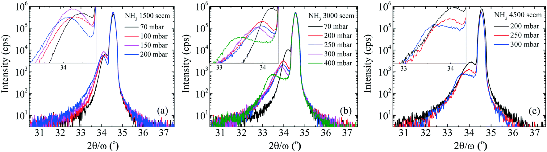 | ||
| Fig. 1 XRD 0002 2θ/ω diffraction patterns of InAl(Ga)N/GaN HSs. InAl(Ga)N layers were grown at (a) 1500 sccm, (b) 3000 sccm, and (c) 4500 sccm NH3 flow under the reactor pressure ranging from 70 to 400 mbar. | ||
With the pressure above 200 mbar for a constant NH3 flow, FWHM of the 0002 diffraction peak of InAl(Ga)N decreased rapidly (shown in Table 1). In our opinion, the effect could be due to improved InN bonding and negligible In-segregation at higher pressure, the otherwise high vapor pressure of N2 over InN leads to the In-segregation and hampers the growth of In-rich InAl(Ga)N. Accompanying the decrement of 0002 FWHM, the FWHM of 101 was almost constant. These values of 0002 and 101 FWHM can be used to estimate the screw and edge threading dislocation densities according to1
 | (1) |
0 diffraction is obtained by the extrapolation of 0002 and 101 FWHM, bs(e) is the magnitude of the Burgers vector of screw (edge) dislocations, and K = 1/(2·π·ln2). Therefore, it can also be stated that with the increase of reactor pressure from 200 to 400 mbar for a constant NH3 flow, the screw dislocation densities decreased from 1010 to 109 cm−2, though the edge dislocation densities were constant ∼1011 cm−2. This indicates that the edge dislocation density in these InAl(Ga)N layers is insensitive to reactor pressure. We believe that the layers with the threading dislocations above 108 cm−2 can induce local strain field variations that locally change the incorporation of the larger size and easily drive In-atoms during the growth.
A2. Reactor pressure vs. surface quality
To investigate the impact of pressure on the surface morphology of InAl(Ga)N layers, AFM and SEM measurements were performed and the results confirm the mass transport growth regime. The growth at the temperature of 730 °C reinforces the kinetics of chemical reactions and the surface mobility of adsorbed atoms. Henceforth, the epitaxial growth rate is controlled by the mass transport of reactants, followed by the diffusion to the growing vapor-solid interface. SEM images of the representative samples' surfaces are shown in Fig. 2 and exhibit granular features that are caused by 3D islands growth mode typical for InAl(Ga)N layers grown by MOCVD. The size of these grains and consequently, the surface roughness of a sample depend on the growth parameters. With the increase of pressure, the grain size is reduced, and grain density is increased. This increase in the density of grains is attributed to the increased nucleation density on the substrate at high pressure. The increase of RMS surface roughness is attributed to the bright particles with a height larger than 100 nm and diameter around 200–300 nm. EDX analysis confirmed a higher In content in the particles compared to the surrounding area. This indicates that the particles are adducts formed due to parasitic reactions between the precursors (TMIn, TMAl and NH3) in In-rich growth conditions.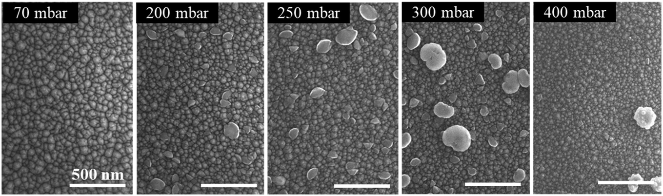 | ||
| Fig. 2 SEM images (white scale bars represent 500 nm) of the top view of InAl(Ga)N layers grown at 70, 200, 250, 300, and 400 mbar pressure and constant NH3 flow of 3000 sccm with RMS surface roughness values of 6, 10.5, 15, 27.5 and 16.8 nm over the scanned area of 5 × 5 μm2, respectively. | ||
A3. Reactor pressure vs. optical properties
Fig. 3 shows the five typical traces of time-resolved in situ optical reflectance during the growth of InAl(Ga)N/GaN HSs with different reactor pressure in InAl(Ga)N layers while keeping NH3 flow constant at 3000 sccm. The traces are divided into four regions corresponding to the four different steps of the whole growth process of InAl(Ga)N/GaN HS on sapphire: (i) The thermal treatment, nitridation of the sapphire substrate, low-temperature GaN nucleation layer and subsequently the coalescence of islands; (ii) the growth of GaN buffer layer; (iii) setting growth conditions for InAl(Ga)N and growth of AlN interlayer; and (iv) the growth of InAl(Ga)N layer. For GaN buffer layers, the reflectivity oscillations with large and equal amplitudes are well resolved, and the simulated thickness is ∼2 μm.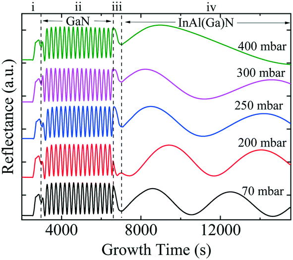 | ||
| Fig. 3 Representative in situ optical reflectance traces (laser wavelength 632.73 nm) of InAl(Ga)N/GaN HSs. InAl(Ga)N layers were grown at different reactor pressure and constant NH3 flow of 3000 sccm. The traces are vertically offset for visibility. | ||
Distinct curves reflectivity in regions (iii) and (iv) with increasing reactor pressure demonstrate the different interface and InAl(Ga)N layer properties, respectively. The reflectance is a function of the surface roughness and refractive index, which depends on the chemical composition of the material. At the end of region (iii), reflectance increased with pressure. At the used pyrometer wavelength (632.7 nm), the trend in the refractive index of binaries is InN > GaN > AlN.16 Therefore, we believe that the increased Al content at the interface could be a possible reason for the increased interface roughness due to the low surface mobility of Al. Consequently, the low refractive index leads to the lower observed reflectance at 70 mbar. With increasing reactor pressure, more incorporation of In and/or Ga influence reflectance. With increasing reactor pressure, the growth rate and consequently, the thickness of InAl(Ga)N layers decreases. The approximate thicknesses of InAl(Ga)N layers are presented in Table 1. This decreasing thickness trend corroborates the loss of precursors in the form of gas-phase parasitic reactions and formation of adducts as shown in Fig. 2.
PL and absorption spectra of the samples obtained at room temperature are shown in Fig. 4(a) and (b), respectively. With the increase of pressure from 70 mbar to 200 mbar, the red-shifted PL peak accompanies the reduced PL intensity. This indicates, that besides the edge dislocation some other factor is also contributing, that causes PL peak shift and related to reactor pressure, unlike ref. 1. For GaN, the absorption edge (AE) was determined by extrapolating the linear region to the baseline, as shown by the dashed line in Fig. 4(b). All samples exhibit distinct GaN AE around 3.42 eV, which is consistent with the measured GaN near band edge (NBE) peak in Fig. 4(a). In PL measurements, inhomogeneities due to compositional fluctuations often lead to the broadening of the emission band. A good example of the broadening is given in ref. 17, where calculations confirm that the alloy fluctuations in InGaN QWs are responsible for the broadening of PL when compared with a QW system without alloy in the active region. It is difficult to determine whether the compositional fluctuation is the dominant effect or if a different mechanism contributes to the broadening of the PL peaks. Toward the low energy side with a reference to the sharp GaN AE, all samples have a broad absorption knee or slowly decreasing absorption up to ∼1.90 eV.
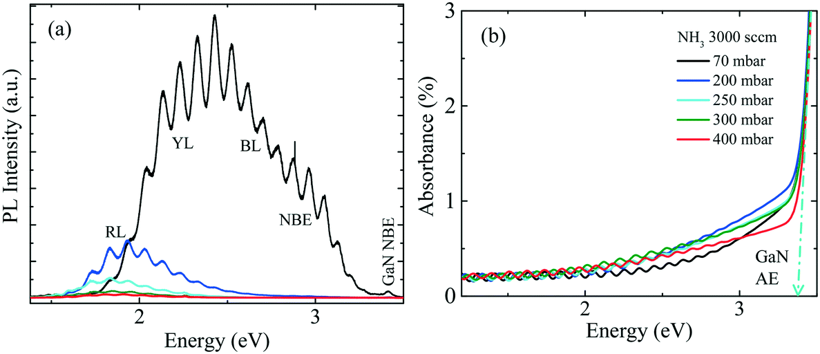 | ||
| Fig. 4 (a) Room temperature PL, and (b) absorbance spectra of InAl(Ga)N/GaN HSs. InAl(Ga)N layers grown at different pressure and constant NH3 flow of 3000 sccm. NBE, BL, YL and RL are abbreviations for near band edge, blue luminescence, yellow luminescence and red luminescence, respectively. (BL: 2.64–2.75 eV, YL: 2.10–2.17 eV, and RL: 1.65–2.00 eV). | ||
As the GaN lies underneath InAl(Ga)N, one would expect most of the light with the photon energy above the bandgap to be absorbed in the InAl(Ga)N, and therefore, the GaN absorption edge would be indiscernible. Since this is not the case, we would surmise that the absorption in the InAl(Ga)N is relatively weak as shown in Fig. 4(b). The broad absorption knees and the substantial change in their shape with the change of reactor pressure confirm a direct absorption in the InAl(Ga)N layers. The absorption is either influenced by the compositional gradient or defects in InAl(Ga)N layers. For quaternary InAl(Ga)N or lnxAlyGa1−x−yN relationship between the chemical composition and bandgap (Eg) is usually stated by utilizing the Vegard's law:1
| Eg(x) = xEg(lnN) + yEg(AlN) + (1 − x − y)Eg(GaN) | (2) |
To gain more insight, the PL and absorption spectra of selected samples are presented in Fig. 5. At 70 mbar, a broad and asymmetric PL peak centered around 2.45 eV with a shoulder at the high-energy side ∼2.96 eV was observed. The deconvolution analysis provides three distinct Gaussian peaks centered around 2.96, 2.45 and 2.12 eV; we assume that these three peaks correspond to the near band edge (NBE), blue luminescence (BL) and yellow luminescence (YL), respectively. In MOVCD growth, carbon (C)-incorporation is higher at the low reactor pressure and C at nitrogen site (CN) and C at interstitial sites (Ci) could be the most probable reason behind BL band transitions.18
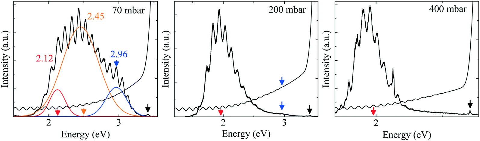 | ||
| Fig. 5 PL and absorbance spectra of InAl(Ga)N/GaN HSs. InAl(Ga)N layers grown at different pressure 70, 200 and 400 mbar while keeping NH3 flow constant at 3000 sccm. The orange and red arrows indicate the advancement of absorption and corresponding PL peak of defects in InAl(Ga)N layer. The blue arrows indicate the absorption edge and PL peak of InAl(Ga)N layers. The black arrow indicate the GaN luminescence peak which conicides with GaN absorption edge. | ||
In our previously reported sample grown at 70 mbar pressure and 1500 sccm NH3 flow,1 we attributed YL band to the transition from shallow donors, V+N and O+N, to deep acceptors, group-III cations vacancies V3−III and their complexes V3−III − O+N, V3−III − (O+N)2.1 The same attribution will continue for YL of sample grown at 70 mbar pressure and 3000 sccm NH3 flow. However, V3−III may fill up as pressure increased. This is confirmed by the disappearance of YL band and appearance of red luminescence (RL) band at higher pressures, 200 and 400 mbar. At 200 and 400 mbar, the PL peaks are observed at 1.94 eV with FWHM of 8.2 eV and at 1.86 eV with FWHM of 7.9 eV, respectively, which is coinciding with their absorption onset (marked by orange arrow). This 80 meV red-shifted PL peak is accompanied by 94% decreased intensity. Moreover, their tail extends toward the high-energy side. This validates the defect-related radiative recombination and most likely due to the Ga at nitrogen site (GaN).19 Such non-radiative defects quench PL. This suggests the freezing of free carriers from the conduction band occurred at 200 mbar due to trapping at the deep acceptor energy levels.
The broad RL band may be the result of strong electron–phonon interaction due to the recombination of carriers at the deep acceptor level. Electron–hole recombination is accompanied by non-radiative phonon transitions, which we acquired using Raman spectroscopy shown in Fig. 6. High spatial order and long-range translational symmetry in high crystal quality binary semiconductors (such as GaN buffer layer) result in narrow Raman peaks. Alloying of additional elements resulting in ternary and quaternary crystals create spatial disorder responsible for broadening of Raman peaks as observed in studied InAl(Ga)N layers. Table 2 summarizes the InAl(Ga)N Raman phonon modes frequencies and shift with reference to Kang et al.20 Red-shifted E2(TO) mode indicates the increased tensile stress in this layer. We assume this could be due to the presence of Ga in InAlN lattice. The localized wave function of a hole at GaN distorts the atomic symmetry and crystal structure expands outward, as illustrated in Fig. 7. Consequently, A1(LO) polar phonon modes are influenced due to the modified intrinsic electric field.21
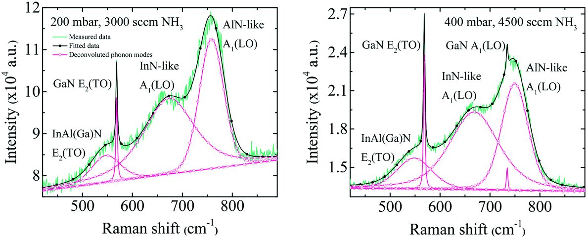 | ||
Fig. 6 Raman spectra of InAl(Ga)N layers grown at 200 and 400 mbar reactor pressure. Spectra were obtained in z(xx)![[z with combining macron]](https://www.rsc.org/images/entities/i_char_007a_0304.gif) backscattering geometry. GaN buffer-related GaN E2(TO) Raman phonon mode in both samples was observed at 568.3 cm−1 and GaN A1(LO) phonon mode was observed at 734.7 cm−1. Latter was observed only in 400 mbar-grown sample due to the strong luminescence background and resulting lower signal to noise ratio in comparison to 200 mbar-grown sample. backscattering geometry. GaN buffer-related GaN E2(TO) Raman phonon mode in both samples was observed at 568.3 cm−1 and GaN A1(LO) phonon mode was observed at 734.7 cm−1. Latter was observed only in 400 mbar-grown sample due to the strong luminescence background and resulting lower signal to noise ratio in comparison to 200 mbar-grown sample. | ||
| InAl(Ga)N Raman phonon modes | Kang et al.20 | This work | ||
|---|---|---|---|---|
| Estimated values for 0.41 In mf (cm−1) | Estimated values for 0.47 In mf (cm−1) | 0.41 In mf/XRD at 200 mbar (cm−1) | 0.47 In mf/XRD at 400 mbar (cm−1) | |
| E2(TO) | 565.6 | 556.3 | 547 (−18.6) | 548 (−8.3) |
| InN-like A1(LO) | 663.2 | 655.0 | 672 (+8.8) | 669 (+14) |
| AlN-like A1(LO) | 771.0 | 755.5 | 758 (−13) | 751 (−4.5) |
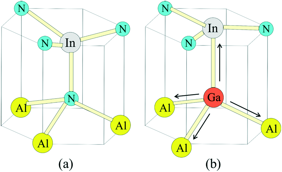 | ||
| Fig. 7 Ball and stick model of (a) InAlN for comparison and (b) GaN defects in InAlN. To represent the symmetry of InAlN, hexagonal prisms are guide for the eye. Note the outwards shift of the surrounding Al atoms and In atom at the presence of GaN defect as pointed by arrows in (b). | ||
B. Role of ammonia flow
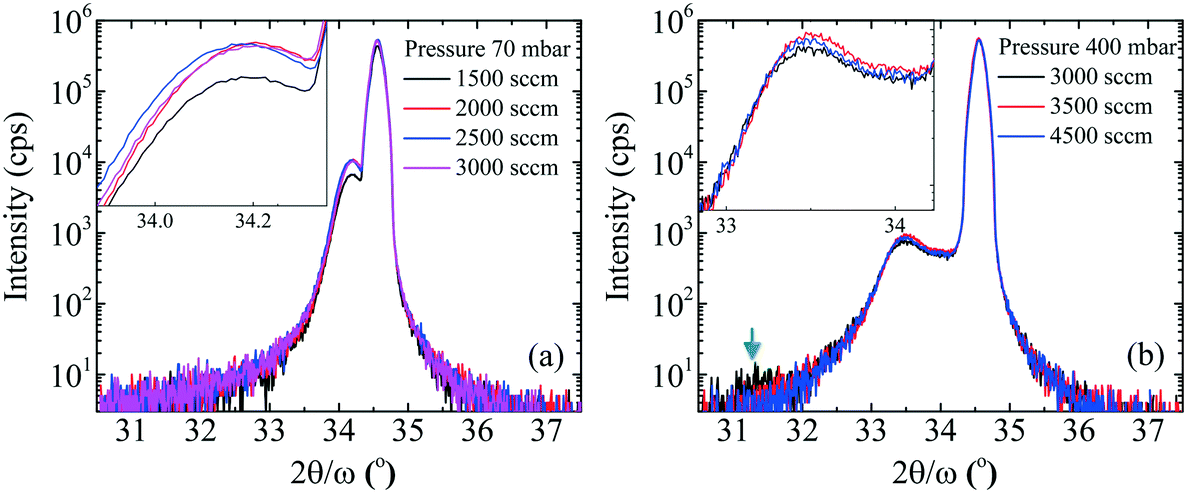 | ||
| Fig. 8 XRD 0002 2θ/ω diffraction pattern of InAl(Ga)N/GaN HSs. InAl(Ga)N layers are grown under (a) 70 mbar, and (b) 400 mbar pressure with NH3 flow ranging from 1500 to 4500 sccm. | ||
B2. Ammonia flow vs. surface morphology
SEM images of the same set of samples are shown in Fig. 9. At the low pressure of 70 mbar and increasing NH3 flow from 1500 to 2000 sccm, increasing the average grain size and surface roughness were observed. A subsequent increase in NH3 flow from 2000 to 3000 sccm, makes the surface smoother due to the progressively increasing coalescence rate. At 200 mbar, the surface roughness increases with the increasing NH3 flow from 1500 sccm to 3000 sccm due to the formation of nano-sized particles similarly observed in Fig. 2.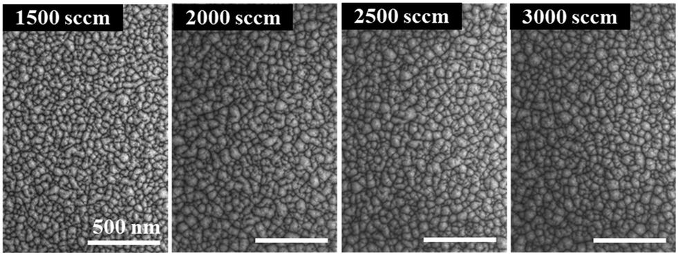 | ||
| Fig. 9 SEM images (white scale bars represent 500 nm) of the top view of InAl(Ga)N layers grown at NH3 flow of 1500, 2000, 2500, and 3000 sccm at constant 70 mbar pressure with RMS surface roughness values of 3.8, 9.5, 8 and 6 nm scanned over the area of 5 × 5 μm2, respectively. | ||
B3. Ammonia flow vs. optical properties
Fig. 10(a) shows four in situ optical reflectance curves during the growth of InAl(Ga)N/GaN HSs with different NH3 flows in InAl(Ga)N layers and the constant pressure at 70 mbar. The InAl(Ga)N layer grown at 1500 sccm NH3 flow exhibits different interface characteristics in comparison with the other samples grown at higher NH3 flows, as shown in region (iii) of the reflectance curve. Subsequently, the low reflectance at the beginning of InAl(Ga)N layer, marked by an arrow in Fig. 10(a), could be due to the high Al content and hence, the slower growth rate in comparison to the others. Increased NH3 flow, improve interface roughness and subsequently surface roughness, as shown in Fig. 9. In Fig. 10(b), broad PL peaks are due to mixed InAl(Ga)N and YL peaks. An increase of NH3 flow from 1500 sccm to 3000 sccm at 70 mbar pressure significantly enhances YL and BL that broadens the PL peak. Kucheyev et al.22 have also reported that oxygen (O) enhances YL and hydrogen (H)-related complexes exhibit blue-shifted broad YL peaks. Thus, our data is consistent with ref. 22, if we assume that NH3 could be the source of moisture (H2O) or O and H impurities.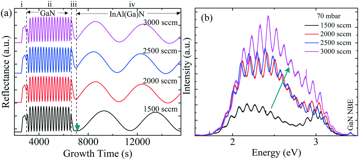 | ||
| Fig. 10 (a) Representative in situ optical reflectance traces (laser wavelength 632.73 nm), and (b) room temperature PL of InAl(Ga)N/GaN HSs. InAl(Ga)N layers are grown at 70 mbar pressure and different NH3 flow. The reflectance traces are vertically offset for visibility. | ||
C. Chemical composition vs. growth parameters
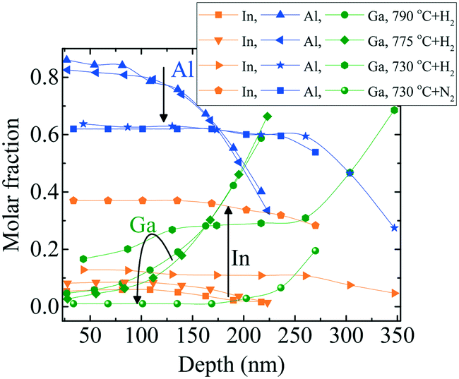 | ||
| Fig. 11 RBS depth profile of InAl(Ga)N layers grown at 70 mbar pressure and 1500 sccm NH3 flow.1 The directed black arrows are guide to the eye and show the influence of decreasing temperature (790 to 730 °C) and carrier gas (H2 to N2 at 730 °C) on depth profile of In-, Al- and Ga-molar fraction. | ||
Fig. 11 illustrates that the decreasing growth temperature from 790 to 730 °C results in a much higher increase in In-molar fraction than Ga-molar fraction. Moreover, with decreasing growth temperature, the growth rate increases, accompanied by increasing Ga-incorporation and decreasing Al-molar fraction. This indicates that Ga replaces Al. However, the growth rate increases to maintain the total amount of Al during deposition. InAl(Ga)N layers are Ga-rich at the interface and with the progression of the growth, layers became Al- rich at the surface. In the InAl(Ga)N layer grown with N2 carrier gas at 730 °C Ga-incorporation decreased. A quaternary InAl(Ga)N layer with ∼50 nm thickness was formed unintentionally at the interface, with Ga decreasing (from 0.19 to 0.01), In increasing (from 0.28 to 0.37) and Al increasing (from 0.54 to 0.62) toward the surface. On the other hand, the subsequent rest of the layer is almost ternary In0.37Al0.63N. This Ga-gradient is much smaller than in the layer grown with H2 carrier gas at 730 °C and at the interface, Ga-incorporation decreased by 72% and Al-incorporation increased by 100% when compared with H2 carrier gas.
C2. Influence of pressure and ammonia flow on Ga-auto-incorporation
To confirm all the assumptions made in sections A and B regarding the chemical compositions in InAl(Ga)N layers, we performed in-depth chemical analysis. Auger depth profiles of InAl(Ga)N layers grown at different pressures and NH3 flows are shown in Fig. 12 to qualitatively and relatively analyze the influence of pressure and NH3 flow on Ga-incorporation profile. Remarkable changes are observed in Ga-auto-incorporation profile with variations in growth parameters. Considering the layer grown at 70 mbar and 1500 sccm NH3 flow as a reference, when NH3 flow doubled, the Ga-incorporation also increased but not significantly, as observed after the growth of 150 nm thick InAl(Ga)N layer. However, when the reactor pressure increased to 200 mbar while keeping NH3 flow at 1500 sccm, the Ga profile shape changed to linear one with the top 100 nm layer having insignificant Ga-incorporation. The layer grown at 200 mbar and 3000 sccm NH3 flow also exhibits linearly decreasing Ga profile toward the surface which is the evidence of NH3 flow preserving the profile shape in contrast to pressure changes. The qualitative AES data are in good agreement with RBS quantitative data. RBS quantitative data confirm the variation in In- and Ga- molar fraction via their linearly increasing and decreasing slopes toward the surface.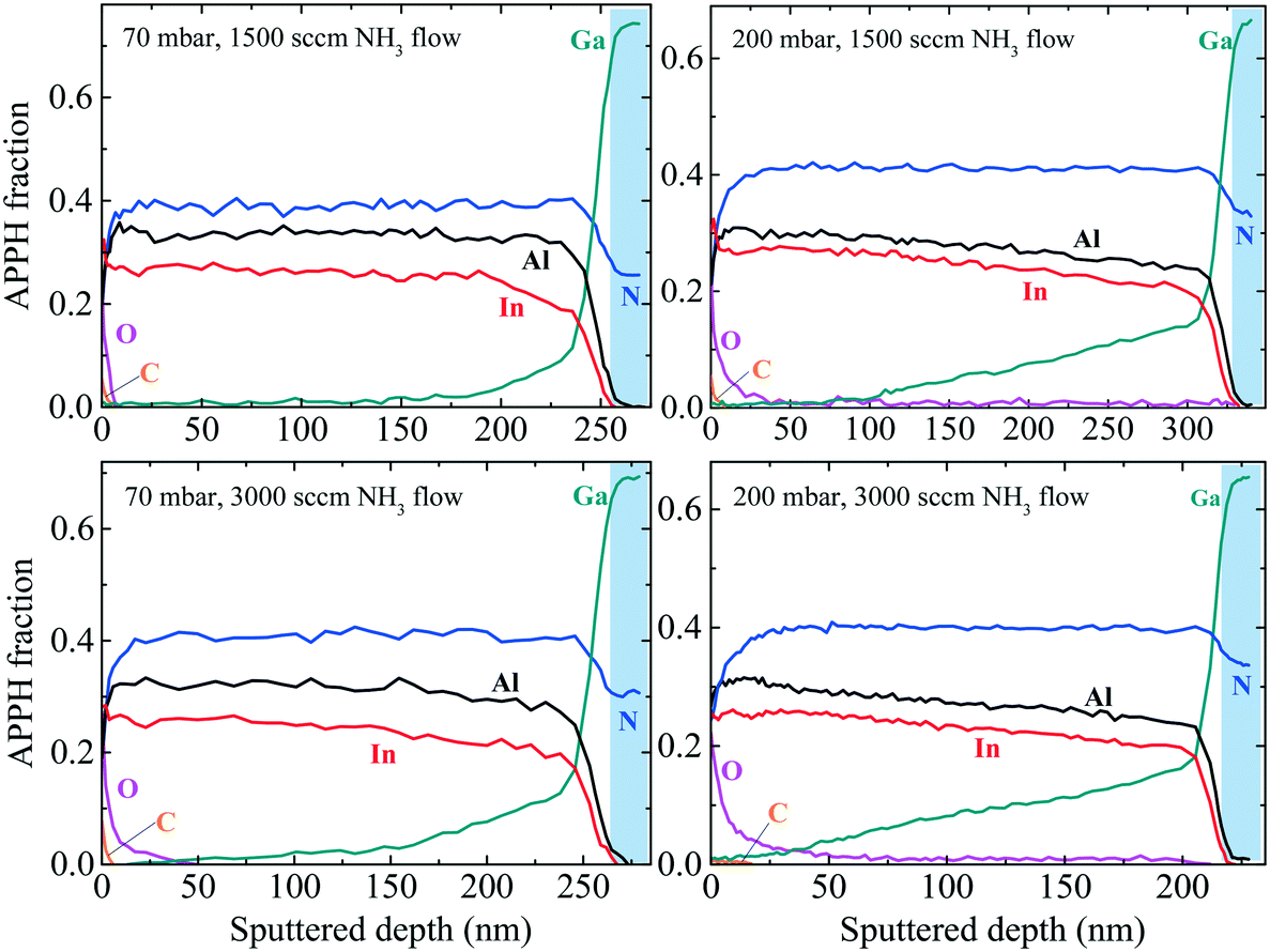 | ||
| Fig. 12 AES depth profile of InAl(Ga)N/GaN HSs. InAl(Ga)N layers are grown at different pressures (70 and 200 mbar) and different NH3 flow (1500 and 3000 sccm) under N2 carrier gas at 730 °C. APPH fraction is defined in ref. 1. Blue color marked the signals from GaN buffer. | ||
The layers grown at 200 mbar, but with 1500 and 3000 sccm NH3 flow include quaternary In0.26Al0.43Ga0.31N and In0.26Al0.46Ga0.34N near GaN buffer, respectively; and In0.42Al0.48Ga0.05N and In0.42Al0.5Ga0.05N located approx. 30 nm below the surface, respectively. At the 3000 sccm NH3 flow, the thickness of InAl(Ga)N layer is 50 nm less and has relatively more Ga- and Al-incorporation. The reduced growth rate could be attributed to the higher Al content as observed in RBS. We conclude that Ga-incorporation increases with increasing reactor pressure. This trend is consistent with the previous report,13 where InAl(Ga)N layer grown at 400 mbar and 4500 sccm NH3 flow was observed with a higher Ga-incorporation. Naturally, thicker InAl(Ga)N layers have a less Ga on top.
The higher NH3 flow produces higher H content, which was confirmed by elastic recoil detection analysis (ERDA). At 200 mbar, the InAl(Ga)N layer grown with 3000 sccm NH3 flow has 3.5% H, while the InAl(Ga)N layer grown with 1500 sccm NH3 flow has only 1%. Increased H or reduced N vacancies could be the possible cause of the reduced free carrier concentration, which is corroborated by the missing blue luminescence (BL) in PL spectra in Fig. 4. This could be attributed to the reactive behavior of H that reduces impurities and passivates the donors (N vacancies). In Fig. 12, variation in O depth profile indicates that either the source of O impurity is NH3 or the surface roughness makes it more exposed to the environmental O, and consequently, more oxidized.23 In the same figure, C is attributed to surface contamination.
To go deeper into details about the influence of reactor pressure and NH3 flow on the growth evolution at nano-level, the layer cross-sections and chemical elements distributions are investigated. Fig. 13 shows the cross-sectional HAADF and BF images along with the corresponding EDX maps for a InAl(Ga)N layer grown at 70 mbar pressure and 1500 sccm NH3 flow (also analyzed in Fig. 11 and 12 by RBS and AES, respectively). The interface layer is quaternary and homogeneous, while the subsequent InAlN layer with 0.37 In-molar fraction exhibits inhomogeneous regions with dark contrast vertical line (In-poor) and void in V-shaped pits, which all together leads to a saw-tooth surface morphology. The quaternary layer appears to have a better crystalline quality possibly due to the presence of Ga, which might enhance miscibility and consequently, suppress phase separation in InAl(Ga)N. A similar cross-section view and features were observed for 500 nm thick InAlN lattice matched to GaN.24
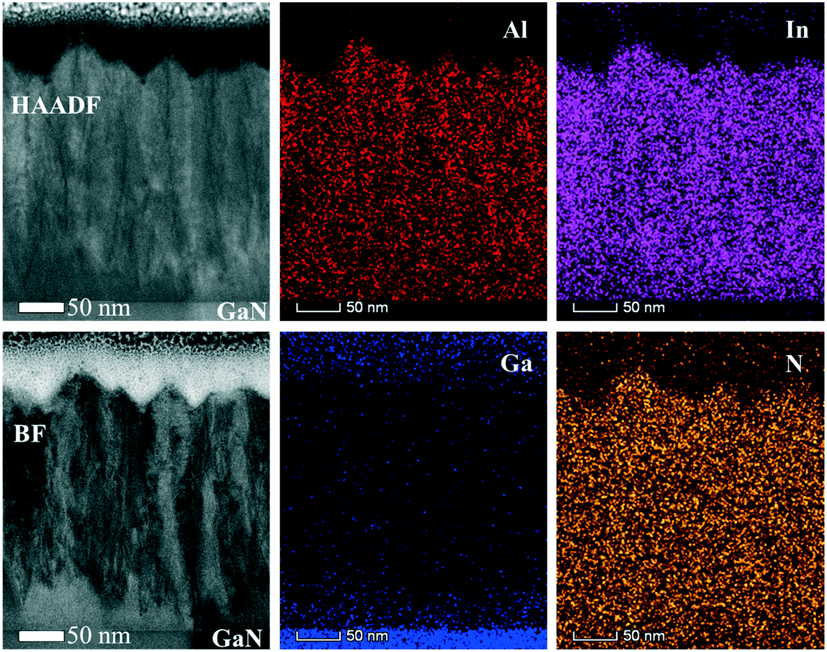 | ||
Fig. 13 HAADF and corresponding BF image (along <11![[2 with combining macron]](https://www.rsc.org/images/entities/char_0032_0304.gif) 0> zone axis) of InAl(Ga)N layer grown under 70 mbar pressure and 1500 sccm NH3 flow. EDX maps of In, Al, Ga and N. HAADF (Z-contrast) shows darker contrast for Ga/Al-rich and brighter contrast for In-rich. 0> zone axis) of InAl(Ga)N layer grown under 70 mbar pressure and 1500 sccm NH3 flow. EDX maps of In, Al, Ga and N. HAADF (Z-contrast) shows darker contrast for Ga/Al-rich and brighter contrast for In-rich. | ||
The surface roughness sensitivity of RBS technique and high channeling due to In-incorporation at preferential sites or random compositional fluctuations at high-pressure growth may underestimate the chemical molar fraction. Due to the limited depth resolution of RBS technique (channel length ∼30 nm), it is difficult to comment on the exact limit where the relaxation takes place in the layer. Hence, for layers grown at ≥200 mbar pressure, the most reliable chemical data could be obtained by the EDX. The HAADF image with EDX analysis reveals that strain relaxation or In-incorporation mechanism is entirely different for layer grown at 200 mbar pressure (shown in Fig. 14). Homogeneous InAl(Ga)N interlayer accommodating strain is also observed, which upon relaxation turned to inhomogeneous. This indicates that the increase in In-incorporation is associated with the strain relaxation in InAl(Ga)N layer, which is consistent with the previous findings.1,2,25,26 At the InAl(Ga)N layer/GaN interface, graded layers allow strain-driven In-incorporation. However, strain relaxation via pit formation due to low surface mobility of Al-adatoms provides favorable incorporation sites for In-adatoms and locally In-molar fraction reaches up to 0.51. Higher growth rate and hence, more compositional fluctuation associated with screw dislocations and/or N-vacancies was observed at 200 mbar in comparison to the layer grown at 400 mbar with a lower growth rate. The EDX data is in good agreement with the chemical trend observed in the absorption spectra, AES and RBS data. This varying chemical depth profile in InAl(Ga)N layer explains the observed broad absorption knee. Reflection at the InAl(Ga)N/GaN interface is also influenced by chemical composition. Furthermore, the growth mechanism changes with the growth pressure and is discussed in the next section.
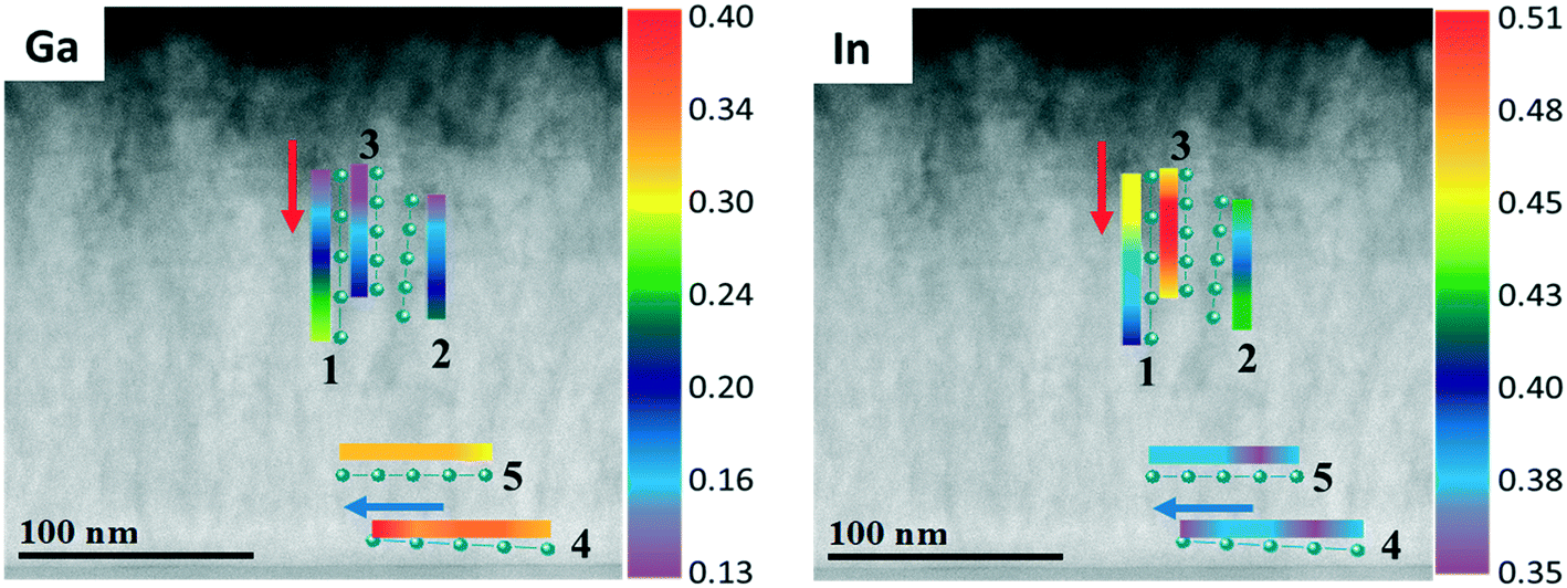 | ||
| Fig. 14 HAADF image (along <110> zone axis)of InAl(Ga)N layer grown at 200 mbar pressure and 3000 sccm NH3 flow, 5 solid lines each with 5 analyzed data points show the position of EDX line scans across the InAl(Ga)N layer. Color bar parallel to each line scan show the corresponding Ga- and In-molar fraction as a function of position. | ||
Discussion
Group-III precursors, used in MOCVD growth of III-Nitrides, in the decreasing order of molar mass (g mol−1) are as follows: TMIn (159.9) > TMAl (144) > TMGa (114.8) (TM = trimethyl, –(CH3)3. Buoyancy-driven convection of the precursors, which is usually in a vertical reactor due to the heated susceptor and cold walls of the reactor, depends on reactor pressure and can create recirculation27 but is less effective at low reactor pressure. TMGa being less dense than other group-III precursors could have a tendency to rise near heated substrate/susceptor and stuck to the colder part of the reactor. This could be the possible reason, the TMGa is creating a memory effect when GaN growth is followed by InAlN layer growth. Another possible source of Ga through inter-diffusion from GaN buffer is ruled out because of the small diffusion ability of Ga atoms in solid, which cannot result in such a high Ga content in InAl(Ga)N. The growth environment has an insignificant amount of contribution to the unintentional Ga incorporated into InAl(Ga)N layers up to ∼200 mbar pressure. However, at the reactor pressure above 200 mbar, the etching or decomposition of GaN buffer under the increased percentage of H2 could emerge as another possible source of Ga besides the growth environment. The possible source of H2 is NH3 pyrolysis at the used growth temperature of 730 °C.Different growth kinetics, local lattice dynamics and growth evolution are demonstrated in Fig. 13 and 14 for InAl(Ga)N layers grown at 70 and 200 mbar reactor pressures, respectively. On that basis, in the following, we will demonstrate the growth mechanism of the InAl(Ga)N layers illustrated in Fig. 15. At low growth pressure, the enhanced surface mobility of Al and poor incorporation efficiency of In form Al-rich InAl(Ga)N layer at the interface. Up-on subsequent layer growth, In replaces Ga and generated compressive strain is released via pits, which are the preferential incorporation sited for In-adatoms and as a result, hillocks occur. For the layer grown at 200 mbar, the pressure enhances In- and Ga-incorporation and the diminishing profile of Ga is benefitted to both In and Al. At this pressure, grains with different In-molar fraction lead to the formation of smaller and denser hillocks. At 400 mbar pressure,13 Al- and/or Ga-rich grains are also formed due to their parasitic reactions and low surface mobility and distributed all over the layer along with the smaller and denser hillocks. In-compositional instability induced by the two thermodynamics factors, i.e. growth temperature, and pressure, is the combined effect of strain and incorporation sites like pits, screw dislocations and rough surface. These sites are generated during the layer growth itself either by higher growth rate or strain relaxation.
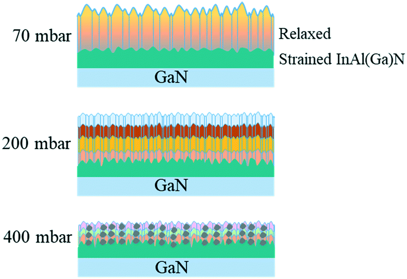 | ||
| Fig. 15 Schematic illustration of the growth of InAl(Ga)N layer at 70, 200 and 400 mbar pressure with 1500, 3000 and 4500 sccm NH3 flow, respectively. Different colors in relaxed layer are representative of different In-molar fractions. At 400 mbar, the grey dots are Al- and/or Ga-rich grains. | ||
Conclusion
The influence of ammonia flow on In-incorporation at fixed pressure is not appreciable. However, high reactor pressure is more favorable to increase In-incorporation with suitably high NH3 flow to provide reactive N species. AES and RBS data confirmed that, changes in pressure and NH3 flow, alter the elemental depth profile within InAl(Ga)N layers. InAlN layer grown under nitrogen carrier gas was observed with 72% lower unintentional Ga-molar fraction at the interface and more than three times higher In-molar fraction in comparison with the layer grown under hydrogen carrier gas but at the growth temperature. The quaternary compositional variation in InAl(Ga)N layers leads to the differences in the PL and absorption spectra. The shape and dimension of the absorption knee depend on the elemental molar fraction and their distribution in InAl(Ga)N, which also depend on growth parameters.Higher pressure is favorable for reducing N vacancies that lead to decreased carrier concentration and photoluminescence. An interesting measurement to investigate this further would be to study the temperature dependence of the PL. At the low temperatures, if the interpretation is correct, the photogenerated carriers may be trapped by the defects in GaN, so we might expect to see the emission from GaN, and less intense emission from the InAl(Ga)N layer.
Conflicts of interest
There are no conflicts of interest to declare.Acknowledgements
The authors would like to acknowledge the financial support granted by the Slovak Agency for R&D: project no. APVV-15-0031 and SK-CN-RD-18-0006. We would also like to acknowledge M. P. Chauvat and P. Ruterana from CNRS France for performing a part of TEM measurement.References
- P. Chauhan, S. Hasenöhrl, E. Dobročka, Ľ. Vančo, R. Stoklas, J. Kováč, P. Šiffalovič and J. Kuzmík, Effect of temperature and carrier gas on the properties of thick InxAl1−xN layer, Appl. Surf. Sci., 2019, 470, 1–7 CrossRef CAS.
- P. Chauhan, S. Hasenöhrl, E. Dobročka, M. P. Chauvat, A. Minj, F. Gucmann, Ľ. Vančo, J. Kováč Jr., S. Kret, P. Ruterana, M. Kuball, P. Šiffalovič and J. Kuzmík, Evidence of relationship between strain and In-incorporation: Growth of thick In-rich InAlN layer by MOCVD, J. Appl. Phys., 2019, 125, 105304 CrossRef.
- B. Reuters, M. Finken, A. Wille, B. Hollander, M. Heuken, H. Kalisch and A. Vescan, Relaxation and critical strain for maximum In incorporation in AlInGaN on GaN grown by metal organic vapour phase epitaxy, J. Appl. Phys., 2012, 112, 093524 CrossRef.
- M. Hiroki, Y. Oda, N. Watanabe, N. Maeda, H. Yokoyama, K. Kumakura and H. Yamamoto, Unintentional Ga incorporation in metalorganic vapor phase epitaxy of In-containing III-nitride semiconductors, J. Cryst. Growth, 2013, 382, 36–40 CrossRef CAS.
- R. Bouveyron and M. B. Charles, Growth by MOCVD of In(Ga)AlN alloys, and a study of gallium contamination in these layers under nitrogen and hydrogen carrier gas, J. Cryst. Growth, 2017, 464, 105–111 CrossRef CAS.
- S.-L. Sahonta, G. P. Dimitrakopulos, T. Kehagias, J. Kioseoglou, A. Adikimenakis, E. Iliopoulos, A. Georgakilas, H. Kirmse, W. Neumann and P. Komninou, Mechanism of compositional modulations in epitaxial InAlN films grown by molecular beam epitaxy, Appl. Phys. Lett., 2009, 95, 021913 CrossRef.
- Q. Y. Wei, T. Li, Y. Huang, J. Y. Huang, Z. T. Chen, T. Egawa and F. A. Ponce, Compositional instability in InAlN/GaN lattice-matched epitaxy, Appl. Phys. Lett., 2012, 100, 092101 CrossRef.
- C. Bazioti, E. Papadomanolaki, T. Kehagias, T. Walther, J. Smalc-Koziorowska, E. Pavlidou, P. Komninou, T. Karakostas, E. Iliopoulos and G. P. Dimitrakopulos, Defects, strain relaxation, and compositional grading in high indium content InGaN epilayers grown by molecular beam epitaxy, J. Appl. Phys., 2015, 118, 155301 CrossRef.
- A. V. Lobanova, K. M. Mazaev, R. A. Talalaev, M. Leys, S. Boeykens, K. Cheng and S. Degroote, Effect of V-III ratio in AlN and AlGaN MOVPE, J. Cryst. Growth, 2006, 287, 601 CrossRef CAS.
- A. V. Lobanova, A. S. Segal, E. V. Yakovlev and R. A. Talalaev, AlInN MOVPE: growth chemistry and analysis of trends, J. Cryst. Growth, 2012, 352, 199 CrossRef CAS.
- R. Bouveyron and M. B. Charles, Growth by MOCVD of In(Ga)AlN alloys, and a study of gallium contamination in these layers under nitrogen and hydrogen carrier gas, J. Cryst. Growth, 2017, 464, 105 CrossRef CAS.
- E. Dobročka, S. Hasenöhrl, P. Chauhan and J. Kuzmík, Non-conventional scans in high-resolution X-ray diffraction analysis of epitaxial systems, Appl. Surf. Sci., 2018, 461, 23 CrossRef.
- S. Hasenöhrl, P. Chauhan, E. Dobročka, R. Stoklas, Ľ. Vančo, M. Veselý, F. Bouazzaoui, M.-P. Chauvat, P. Ruterana and J. Kuzmík, Generation of hole gas in non-inverted InAl(Ga)N/GaN heterostructures, Appl. Phys. Express, 2019, 12(1), 014001 CrossRef.
- D. Iida, K. Nagata, T. Makino, M. Iwaya, S. Kamiyama, H. Amano, I. Akasaki, A. Bandoh and T. Udagawa, Growth of GaInN by Raised-Pressure Metalorganic Vapor Phase Epitaxy, Appl. Phys. Express, 2010, 3, 075601 CrossRef.
- T. Y. Wang, J. H. Liang and D. S. Wuu, Defect formation mechanism and quality improvement of InAlN epilayers grown by MOCVD, CrystEngComm, 2015, 17, 8505–8511 RSC.
- S. Berrahs, H. Abid and A. Boukortt, The first principle calculation of electronic and optical properties of AlN, GaN and InN compounds under hydrostatic pressure, Semicond. Phys., Quantum Electron. Optoelectron., 2006, 9(2), 12–16 CrossRef.
- D. Watson-Parris, M. J. Godfrey, P. Dawson, R. A. Oliver, M. J. Galtrey, M. J. Kappers and C. J. Humphreys, Carrier localization mechanisms in InGaN/GaN quantum wells, Phys. Rev. B: Condens. Matter Mater. Phys., 2011, 83, 115321 CrossRef.
- A. Armstrong, A. R. Arehart, B. Moran, S. P. DenBaars, U. K. Mishra, J. S. Speck and S. A. Ringel, Impact of carbon on trap states in n-type GaN grown by metalorganic chemical vapor deposition, Appl. Phys. Lett., 2004, 84, 374 CrossRef CAS.
- M. A. Reshchikov and H. Morkoç, Luminescence properties of defects in GaN, J. Appl. Phys., 2005, 97, 061301 CrossRef.
- T.-T. Kang, M. Yamamoto, M. Tanaka, A. Hashimoto and A. Yamamoto, Effect of gas flow on the growth of In-rich AlInN films by metal-organic chemical vapor deposition, J. Appl. Phys., 2009, 106, 053525 CrossRef.
- H. Gu, K. Wu, S. Zheng, L. Shi, M. Zhang, Z. Liu, X. Liu, J. Wang, T. Zhou and K. Xu, Redshift of A1(longitudinal optical) mode for GaN crystals under strong electric field, Appl. Phys. Express, 2018, 11, 011002 CrossRef.
- S. O. Kucheyev, M. Toth, M. R. Phillips, J. S. Williams, C. Jagadish and G. Li, Chemical origin of the yellow luminescence in GaN, J. Appl. Phys., 2002, 91, 5867 CrossRef CAS.
- E. L. Piner, M. K. Behbehani, N. A. El-Masry, J. C. Roberts, F. G. McIntosh and S. M. Bedair, Impurity dependence on hydrogen and ammonia flow rates in InGaN bulk films, Appl. Phys. Lett., 1997, 71, 2023 CrossRef CAS.
- G. Perillat-Merceroz, G. Cosendey, J.-F. Carlin, R. Butté and N. Grandjean, Intrinsic degradation mechanism of nearly lattice-matched InAlN layers grown on GaN substrates, J. Appl. Phys., 2013, 113, 063506 CrossRef.
- E. Dobrocka, X-ray diffraction analysis of epitaxial layers with depth-dependent composition, Mater. Struct., 2019, 26, 148 Search PubMed.
- P. Chauhan, S. Hasenöhrl, A. Minj, M. P. Chauvat, P. Ruterana and J. Kuzmík, Growth evolution of N-polar Indium-rich InAlN layer on c-sapphire via strain relaxation by ultrathin AlON interlayer, Appl. Surf. Sci., 2020, 502, 144086 CrossRef CAS.
- L. J. Giling, in Crystal Growth of Electronic Materials, ed. E. Kaldis, Elsevier Science, Amsterdam, 1985, pp. 71–86 Search PubMed.
| This journal is © The Royal Society of Chemistry 2020 |