
Hierarchical growth and morphological control of ordered Cu–Au alloy arrays with high surface enhanced Raman scattering activity†
Zhezhe
Wang
 abcd,
Ruihua
Liu
a,
Zhuohong
Feng
abc,
Lin
Lin
abc,
Rongrong
Xie
e,
Jiabing
Li
de,
Heguang
Liu
f,
Feng
Huang
*abc and
Zhiqiang
Zheng
*abc
abcd,
Ruihua
Liu
a,
Zhuohong
Feng
abc,
Lin
Lin
abc,
Rongrong
Xie
e,
Jiabing
Li
de,
Heguang
Liu
f,
Feng
Huang
*abc and
Zhiqiang
Zheng
*abc
aCollege of Physics and Energy, Fujian Normal University, Fuzhou, 350117, China. E-mail: fengh@fjnu.edu.cn; zqzheng@fjnu.edu.cn
bFujian Provincial Key Laboratory of Quantum Manipulation and New Energy Materials, Fuzhou, 350117, China
cFujian Provincial Collaborative Innovation Center for Optoelectronic Semiconductors and Efficient Devices, Xiamen, 361005, China
dSchool of Plant, Environmental and Soil Sciences, Louisiana State University, Baton Rouge, LA 70803, USA
eCollege of Environmental Science and Engineering, Fujian Normal University, Fuzhou 350007, China
fSchool of Materials Science and Engineering, Xi'an University of Technology, Xi'an, 710048, China
First published on 10th November 2019
Abstract
Low-cost Cu–Au alloy hierarchical structures are fabricated by coelectrodeposition, and the highest SERS activity is obtained when the atom ratio of Cu and Au is about 88![[thin space (1/6-em)]](https://www.rsc.org/images/entities/char_2009.gif) :12. The effect of morphology of Cu–Au alloys on the SERS performance is investigated, and the corresponding SERS spectra and FDTD results show that multi-branched Cu–Au dendrites exhibit the highest SERS activity for the massive Raman “hot spots”, especially when the dendrites are self-assembled on highly ordered Si pillar substrates. Using the multi-branched Cu–Au alloy arrays, Rhodamine 6G (R6G) with a trace concentration as low as 10−14 M can be detected, and the enhancement factor (EF) is estimated to be about 6 × 10¹⁰.
:12. The effect of morphology of Cu–Au alloys on the SERS performance is investigated, and the corresponding SERS spectra and FDTD results show that multi-branched Cu–Au dendrites exhibit the highest SERS activity for the massive Raman “hot spots”, especially when the dendrites are self-assembled on highly ordered Si pillar substrates. Using the multi-branched Cu–Au alloy arrays, Rhodamine 6G (R6G) with a trace concentration as low as 10−14 M can be detected, and the enhancement factor (EF) is estimated to be about 6 × 10¹⁰.
Introduction
Raman scattering has been considered to be a powerful technique for the trace detection and recognition of analytes due to its excellent fingerprint effect, which is of great interest for many applications including chemical analysis, food quality control, environmental monitoring and biomolecular detection.1–5 However, Raman signals for molecules are very weak for small scattering cross sections, generally in the range of 10−30–10−25 cm2.6 For enhancing the scattering signal, the tested molecules are usually attached to the rough surface of some noble metal nanostructures, which would extremely enhance the spectral intensity by several orders of magnitude and even enable single-molecule detection. At present, various metallic nanostructures like silver (Ag), gold (Au) and copper (Cu) have been reported as superior SERS substrates, especial their alloys.7–13Alloys, defined by a metallic bonding character, could reduce the overall cost of the materials while preserving important properties. Many reports have shown that bimetal alloys show higher SERS activity than pure metals.14–16 For example, Hwang and Dong Qin have reported that the SERS activity of Au/Ag composite structures was larger than that of similar structures made of pure Au or Ag, respectively.17,18 Moreover, the SPR absorbance of Au–Ag alloys is tunable via changing their properties.19 At present, various Au–Ag alloys with different morphologies, such as Ag–Au alloy nanospheres, nanoboxes, and sponge-like porous Ag–Au alloys, have been prepared and exhibited an intense electric field enhancement, larger specific surface area, and tunable plasmonic coupling.20–22 In particular, when the alloys are processed into ordered arrays, the SERS activity and repeatability could be improved effectively.23,24 Metal Cu also has a strong plasmonic effect but suffers from instability due to oxidation effects. However, the Cu–Au alloys have incomparable superiority over single metals because of their low-cost and chemically/mechanically stability. Jian Chen has reported the Cu–Au alloy nanowire SERS substrates for detecting R6G with a concentration as low as 10−15 M.25
Therefore, in this paper, considering its low-cost and repeatability, Cu–Au alloys will be fabricated by coelectrodeposition. Their composition and morphology will be adjusted by tuning the electrolyte and controlling the nucleation and growth processes. And the effect of the composition and morphology on the alloys' SERS activities is studied in order to determine the optimal SERS. Finally, multi-branched dendritic Cu–Au alloys with massive Raman “hot spots” are deposited on highly-ordered silicon pillar arrays assisted by self-assembly. Our studies show a fascinating but easy preparation approach for Cu–Au alloy SERS substrates due to the lower oxidation–reduction potential (ORP) (see Table S1 in the ESI†), and moreover, the lower interband transition threshold of Cu (1.9 eV) could potentially enhance the alloys' interband transitions, hence improving their optical properties,26,27 which is very promising for the actual application of the SERS substrates for trace concentration detection with high efficiency.
Experimental
The fabrication procedure (as shown in Fig. S1†), morphology characterization and SERS measurements for the Cu–Au alloy arrays are both described in the ESI.† However, the materials used in this study are as follows: a positive photoresist (AZ MiR (TM) 701) and a developer were purchased from AZ Electronic Materials. Hexamethyldisilazane (AR 99%, HMDS) was purchased from Macklin, China. Tetrachloroauric(III) acid tetrahydrate (HAuCl4·4H2O), copper(II) chloride (CuCl2), sodium sulfite (Na2SO3), dipotassium hydrogen phosphate (K2HPO4), ethylenediaminetetraacetic acid (EDTA) and rhodamine 6G (R6G) were purchased from Sinopharm Chemical Reagent Co., Ltd. All the silicon wafers are chemically cleaned and heated to remove contaminants and moisture on the wafer surface and all the preparation processes are carried out on a clean booth station.Results and discussion
The flower-like Cu–Au alloys prepared by coelectrodeposition are shown in Fig. 1c. And the contrast SERS spectra of Cu–Au alloys with Au and Cu with an almost identical morphology (Fig. 1a and b) are measured as shown in Fig. 1d, which shows that the Cu–Au alloys exhibit higher SERS activity than both pure Cu and Au. That is because the charge-transfer between Cu and Au atoms in the alloys can create positively charged domains rich in one atom and negatively charged regions dominated by another atom, and this charge-transfer induced aggregation is favorable at certain Cu:Au ratios.27
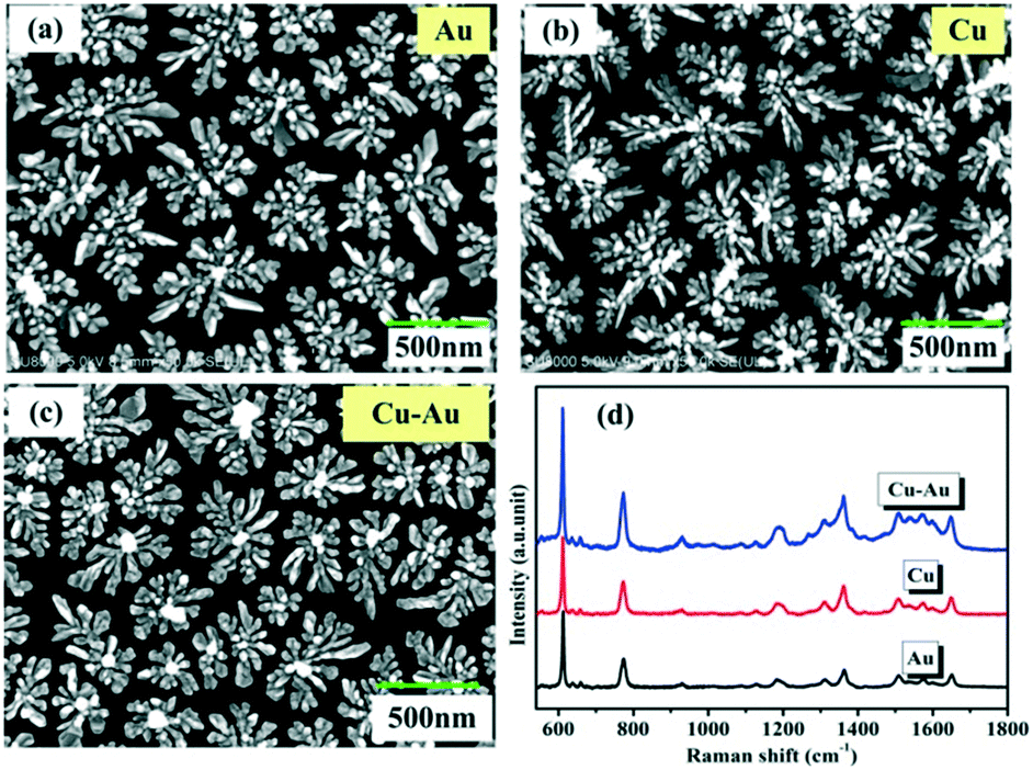 | ||
| Fig. 1 (a)–(c) The SEM images of Au, Cu and Cu–Au alloys prepared by coelectrodeposition. (d) The contrast SERS spectra of Au, Cu and Cu–Au alloys corresponding to (a)–(c), respectively. | ||
The Cu:Au ratios of the alloys can be adjusted via changing the electrolyte composition. Fig. 2a shows the Raman spectra of Cu–Au alloys with different molar ratios of Cu2+ and Au3+ in the electrolyte solution. Here, 10−5 M R6G is used as probe molecules and the laser excitation wavelength is 532 nm. Several characteristic bands of R6G are clearly detected, where the peaks centered at 612 cm−1 and 1571 cm−1 are assigned to the C–C–C and C–O–C bond stretching vibrations, respectively. The peaks at 1311 cm−1, 1361 cm−1, 1509 cm−1 and 1648 cm−1 correspond to the C–C stretching modes and the peak at 775 cm−1 is attributed to the out-of-plane vibration of the deformed C–H bonds.28 From Fig. 2a, it can be seen that the SERS activity achieves maximum enhancement, when the molar ratio of Cu2+:Au3+ in the electrolyte is about 1:1.5. In this state, the energy dispersive X-ray spectrometry (EDS) spectrum (Fig. 2b) shows that the prepared alloy did contain Cu and Au, and the further measured inductively coupled plasma (ICP) result indicates that the final atom ratio of Cu and Au in the Cu–Au alloys with the best SERS activity is about 88:12. The corresponding high resolution transmission electron microscopy (HRTEM) image of one of the branches of the Cu–Au alloy is shown in Fig. 2c, and the measured lattice spacing is estimated to be about 0.23 nm, which matches with the {111} plane of CuAu(I) solid solution (PDF#25-1220). Moreover, the formation of the Cu–Au alloys is further demonstrated using the HRTEM images and the work function of Au, Cu and Cu–Au alloy, as shown in Fig. S3 and S4 in the ESI.†
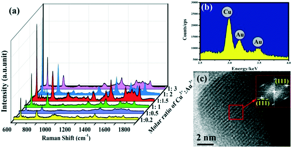 | ||
| Fig. 2 (a) SERS spectra of the Cu–Au alloy with different composition ratios, (b) the EDS spectrum of the Cu–Au alloy and (c) the TEM image of one of the branches of the alloy; inset is the fast Fourier transform (FFT) pattern taken from the marked region in (c). | ||
The morphology of the Cu–Au alloy is precisely tuned by controlling the nucleation and growth processes via adjusting the applied voltage, which plays a vital role in the SERS activity. The regulation mechanism can be illustrated with the schematic drawing in Fig. 3, from which it can be deduced that the elevated applied voltage results in numerous but very small grains, as shown in Fig. 3a and b, which will grow rapidly into approximately spherical alloys, as shown in the SEM image in Fig. 3c. In contrast, with lower applied voltage, fewer and bigger nucleated grains are obtained as shown in Fig. 3d, and the lower voltage also facilitates the anisotropic growth and formation of fractal flower-like alloys (see Fig. 3e).
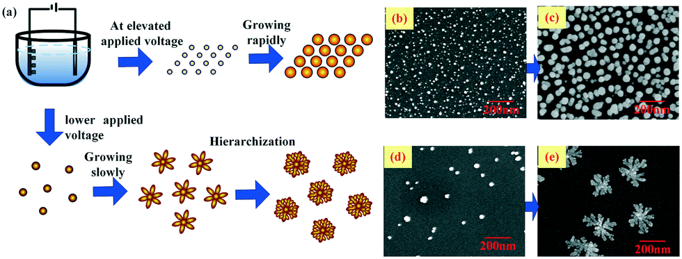 | ||
| Fig. 3 (a) Schematic drawing of the regulation mechanism of the Cu–Au alloys and (b)–(e) the SEM images of the Cu–Au alloys with different applied voltages and reaction times, respectively. | ||
The microscopic mechanism of the morphology regulation can be explained by electrocrystallization. During the electrodeposition of the Cu–Au alloy, a certain overvoltage must be required to provide the energy for the nucleation of the alloys to transform from the liquid phase into the solid phase.29 The relationship between the cathodic overvoltage (ΔφK) and the change of free energy (ΔG) can be expressed in the following equation:
| ΔG = −πr2hρnFΔφKM−1 + 2πrhσ1 + πr2(σ1 + σ2 + σ3) | (1) |
From eqn (1), it can be seen that there is a critical radius (rc), over which the nucleation could be stabilized. The rc can be derived as the following:
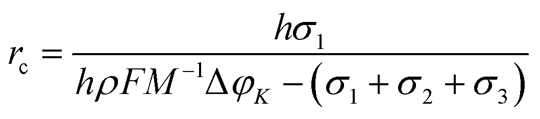 | (2) |
Moreover, the nucleation rate (V) is also related to ΔφK, as shown in eqn (3).
 | (3) |
Therefore, the excessive ΔφK, which is proportional to the applied voltage, results in the increase of nucleation rate and the decrease of critical radius, and thus, numerous small grains are obtained and vice versa.
A series of experiments with different voltages have been carried out and the corresponding morphologies have been determined, as shown in Fig. 4a. The successive applied voltages are 2 V, 6 V, 8 V, 10 V, 12 V, 14 V and 16 V from left to right, respectively. From Fig. 4a, it can be obviously seen that there is a critical voltage (about 10 V). At a voltage lower than which, the fractal dimension of the Cu–Au alloys increases with the applied voltage, while at a voltage higher than 10 V, the fractal dimension decreases gradually. According to the diffusion limited aggregation (DLA) model, it can be concluded that with the increase of the voltage, the number of reduced particles increases, while the random walking particles are easily captured by the exposed ends of the growing clusters, and thus the hierarchical growth of the Cu–Au alloy becomes increasingly obvious.30 Otherwise, at voltages higher than 10 V, the sizes of the nuclei are reduced and the growth rate is accelerated. Because there are no preferential angles that could be selected by the reduced particles, the clusters are most prone to grow isotropically.31
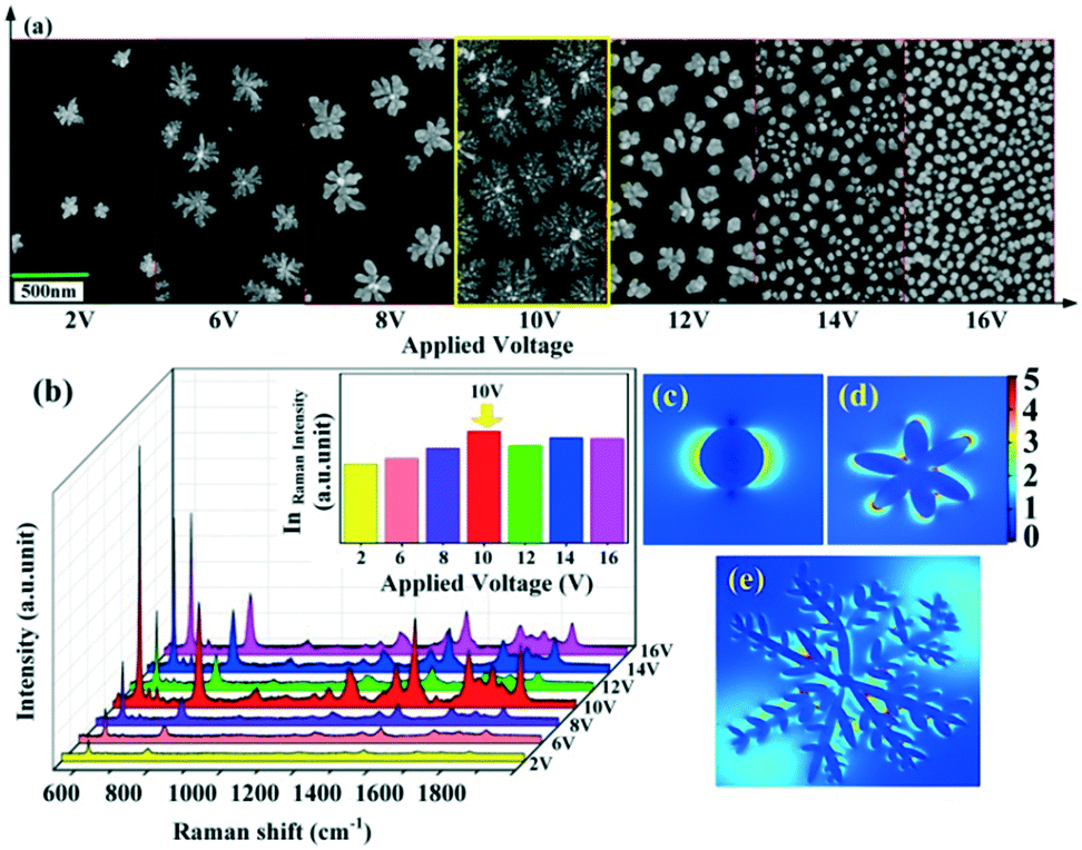 | ||
| Fig. 4 SEM images, SERS spectra and 3D FDTD simulations of the Cu–Au alloys with a Cu2+:Au3+ molar ratio of 1:1.5 and a deposition time of 10 min. (a) The SEM images of the Cu–Au alloys prepared with different applied voltages, respectively. The scale bar of all the SEM images is 500 nm. (b) SERS spectra of the as-prepared Cu–Au alloys probed with 10−5 M R6G corresponding to (a). The inset is the histogram illustrating the dependence of Raman intensity on the applied voltage during growth. (c)–(e) The spatial distribution of the electric field obtained by 3D FDTD simulations for the spherical, flower-like and dendritic Cu–Au alloys, respectively. | ||
The SERS spectra of the Cu–Au alloys in Fig. 4b show that the strongest Raman enhancement is achieved at 10 V, because such dendritic nanostructures can provide a large number of “hot spots” at the end of branches or the junctions of adjacent branches.32 This enhancement can also be deduced from the theoretical simulation of electric field spatial distribution simulated by three dimensional finite-difference time-domain (3D FDTD) simulations. Fig. 4c–e show the spatial distribution of electric field for the spherical, flower-like and dendritic Cu–Au alloys, respectively. It can be obviously seen that the electromagnetic field (EM) enhancement in the nanogaps generated from the branches of the dendritic nanostructure is much larger than that from the spherical-like nanostructure, which enable the dendritic Cu–Au alloys with the branched morphology having the highest SERS activities.
Micromorphology can also be tailored by adjusting the concentration of metal ions in the electrolyte. Fig. 5a–f show the SEM images of the Cu–Au alloys with Cu2+ concentrations of 0.025 mM, 0.50 mM, 0.80 mM, 1.00 mM, 1.50 mM and 2.00 mM, respectively, where the molar ratio of Cu2+:Au3+ is maintained at 1:1.5. From Fig. 5, it can be seen that there is a threshold for the hierarchical growth of the Cu–Au alloys, above which the flower-like dendrite structures almost disappear. According to the theory of electrocrystallization, there is an inferior limit of current density under which the hierarchical growth can be improved with the increase of the current density. Meanwhile, over this inferior limit, the overvoltage will increase with the increase of the current density, which is beneficial for the nucleation and isotropic growth. Thus, fine and spherical Cu–Au alloys are formed. The relationship of current density and concentration of metal ions can be expressed by the following Cottrell equation:
 | (4) |
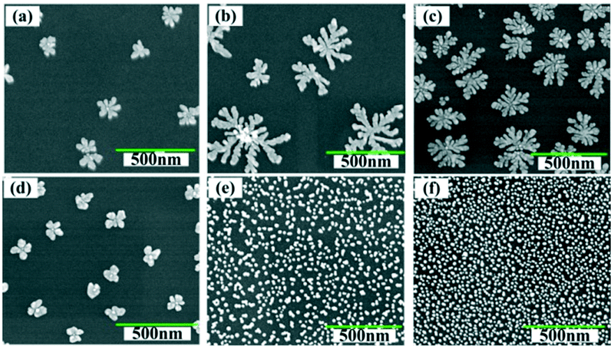 | ||
| Fig. 5 SEM images of the Cu–Au alloys with a Cu2+:Au3+ molar ratio of 1:1.5 and a deposition time of 10 min. Here, (a)–(f) show the SEM images of the Cu–Au alloys prepared with different concentrations of metal ions, and the corresponding concentration of Cu2+ is 0.025 mM, 0.50 mM, 0.80 mM, 1.00 mM, 1.50 mM and 2.00 mM, respectively. The scale bar of all the SEM images is 500 nm. | ||
The SERS spectra of the as-prepared Cu–Au alloys probed with 10−5 M R6G with different concentrations of metal ions are measured and the results are shown in Fig. 6. The SERS activity of the Cu–Au alloys with a Cu2+ concentration of 0.8 mM is the best, which is in accordance with the result of the FDTD. That is the dense and multi-branched morphology can provide the most Raman “hot spots” and enable the dendritic Cu–Au alloys to have the best enhancement effect.
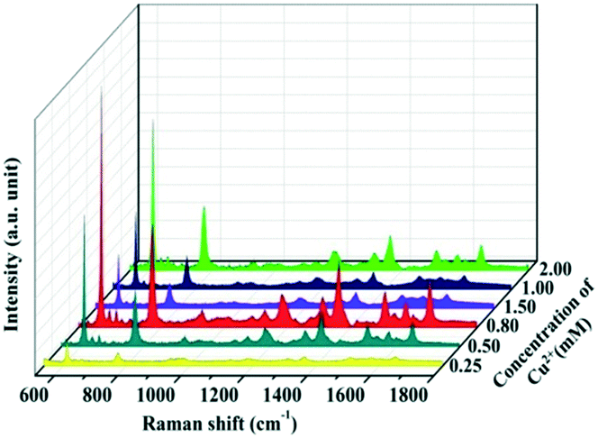 | ||
| Fig. 6 The SERS spectra for the as-prepared Cu–Au alloys probed with 10−5 M R6G with different concentrations of metal ions, and the corresponding concentration of Cu2+ is 0.25 mM, 0.50 mM, 0.80 mM, 1.00 mM, 1.50 mM and 2.00 mM, respectively. The molar ratio of Cu2+:Au3+ in all the samples is 1:1.5 and the deposition time is 10 min. | ||
The growth and ripening process of the Cu–Au alloys with different deposition times of 5 min, 10 min, 15 min and 25 min is observed as shown in Fig. 7a–d, where the applied voltage is 10 V. During this process, the reduced alloys grow and become denser with time. However, if the deposition time is as long as 25 min, the dendritic Cu–Au alloys will ripen and a few large dendrites appear and elongate into the space perpendicular to the substrate (see Fig. 7d). Without the bound substrate, these extremely large dendrites will fall off in the subsequent cleaning process, which will give rise to the decrease of the SERS activity, as seen in Fig. 7e.
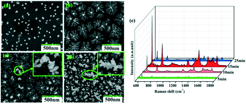 | ||
| Fig. 7 SEM images and SERS spectra of the Cu–Au alloy on the silicon pillar substrate prepared with different deposition times. The time for (a)–(d) is 5 min, 10 min, 15 min and 25 min, respectively. The scale bar of all the SEM images is 500 nm. Insets are the corresponding amplified images. (e) shows the SERS spectra corresponding to the Cu–Au alloys probed with 10−5 M R6G at different deposition times. | ||
Finally, we processed the Cu–Au alloy hierarchical structure onto the highly ordered Si pillar arrays. Fig. 8a shows the contrast SERS spectra between the Cu–Au alloys processed on the ordered pillar arrays and on the flat wafer, from which it can be seen that the Cu–Au alloy arrays have a stronger Raman signal than the flat ones because the extremely rough surface of the highly ordered arrays could adsorb more R6G probe molecules. Meanwhile, the SERS spectra of 10−5 M R6G adsorbed on the top and bottom of the Cu–Au arrays are measured respectively and the result is shown in Fig. 8b. The SERS enhancement is mainly from the tops of the Cu–Au alloy arrays.
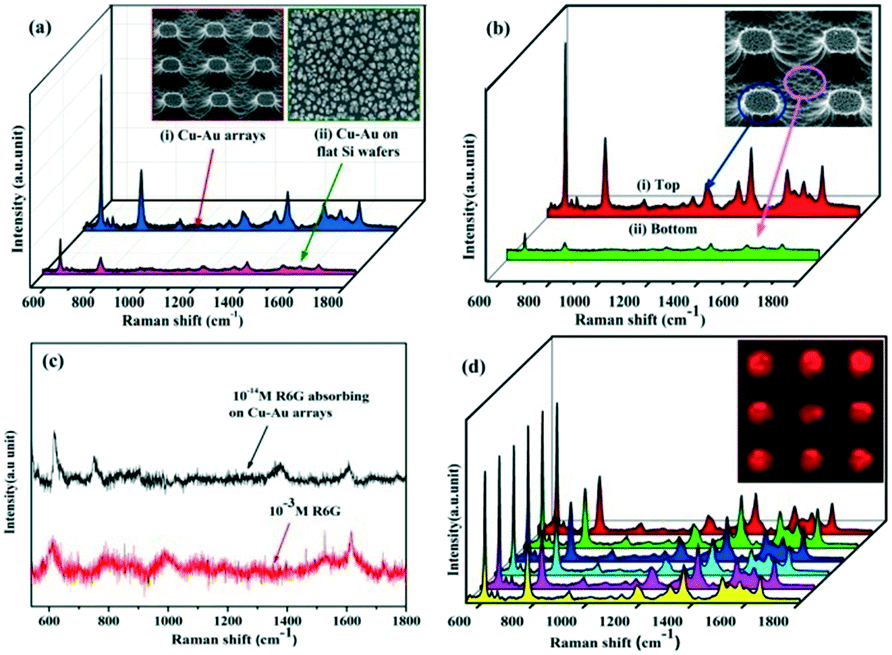 | ||
| Fig. 8 SERS spectra of the as-prepared Cu–Au alloy arrays. (a) The contrast SERS spectra of the Cu–Au alloy prepared on the Si pillar arrays and the flat Si wafer, respectively. (b) SERS spectra of different areas of the Cu–Au alloy arrays. (c) SERS spectra of 10−14 M R6G adsorbed on the Cu–Au arrays (black curve) and the normal Raman spectra of 10−3 M R6G (red curve), respectively. (d) SERS spectra of 10−5 M R6G obtained at 6 randomly chosen spots from the sample, showing the good reproducibility of the SERS signals of the as-prepared Cu–Au alloy arrays, where the inset image is the Raman mapping of R6G at 612 cm−1. | ||
In order to estimate the enhancement factor (EF) of the Cu–Au alloy arrays, the SERS spectrum of 10−14 M R6G adsorbed on the Cu–Au arrays and the normal Raman spectrum of 10−3 M R6G are measured, respectively (as seen in Fig. 8c). The calculated formula is as follows:33
| EF = (ISERS/NSERS)/(INormal/NNormal) |
Furthermore, the reproducibility of the SERS signals has been also tested, as seen in Fig. 8d, which shows the SERS spectra of 10−5 M R6G adsorbed on 6 randomly chosen spots from the sample. The homogeneous distribution of the Raman intensity strongly proves that the SERS substrates are uniform and the generated SERS signals exhibit good reproducibility. The inset image shows the Raman mapping of R6G at 612 cm−1 adsorbed on a certain Cu–Au alloy arrays, which also shows that the distribution of the Raman intensity on the ordered pillars is very uniform.
Conclusions
In this work, aiming for SERS application for trace detection, Cu–Au alloy hierarchical structures are fabricated using coelectrodeposition. The nucleation and growth processes of the product are investigated, which are affected by the precursor concentrations and composition and applied voltage during the electrochemical reaction. To optimize the SERS properties, the optimal atom ratio of Cu and Au is chosen as 56:44. And the morphology with the most branched structures is found to be beneficial to the SERS signals owing to the large number of ‘hot spots’. Finally, the Cu–Au alloys have been processed onto the highly ordered Si pillar arrays, and the EF of these Cu–Au alloy arrays with good reproducibility is estimated to be about 6 × 10¹⁰, which can be regarded as very highly-sensitive SERS substrates, even qualified for single-molecule detection.
Conflicts of interest
There are no conflicts to declare.Acknowledgements
The authors acknowledge the financial support from the National Natural Science Foundation of China (No. 51202033 and 11204039), the Natural Science Foundation of Fujian Province of China (No. 2016J01213, 2017J01399 and 2019J01283) and the Fujian Provincial Orienting Sci & Tech Project (2018H0012).References
- T. Chen, H. Chen, H. Wang, G. Chen, Y. Wang, Y. Feng, W. S. Teo, T. Wu and Hongyu Chen, ACS Nano, 2010, 4, 3087–3094 CrossRef CAS PubMed.
- H. Tang, G. Meng, Q. Huang, C. Zhu, Z. Huang, Z. Li, Z. Zhang and Y. Zhang, RSC Adv., 2014, 4, 19654–19657 RSC.
- V. Sharma and V. Krishnan, Sens. Actuators, B, 2018, 262, 710–719 CrossRef CAS.
- F. Jia, X. Yu and L. Zhang, J. Power Sources, 2014, 252, 85–89 CrossRef CAS.
- K. Yuan, J. Zheng, D. Yang, B. Sánchez, X. Liu, X. Guo, C. Liu, N. Dina, J. Jian, Z. Bao, Z. Hu, Z. Liang, H. Zhou and Z. Jiang, ACS Omega, 2018, 3, 2855–2864 CrossRef CAS PubMed.
- X. Li, Y. Zhang, Z. Shen and H. Fan, Small, 2012, 8, 2548–2554 CrossRef CAS PubMed.
- B. Chen, G. Meng, Q. Huang, Z. Huang, Q. Xu, C. Zhu, Y. Qian and Y. Ding, ACS Appl. Mater. Interfaces, 2014, 6, 15667–15675 CrossRef CAS PubMed.
- D. Liu, C. Li, F. Zhou, T. Zhang, H. Zhang, X. Li, G. Duan, W. Cai and Y. Li, Sci. Rep., 2015, 5, 7686 CrossRef CAS PubMed.
- C. Zhu, G. Meng, P. Zheng, Q. Huang, Z. Li, X. Hu, X. Wang, Z. Huang, F. Li and N. Wu, Adv. Mater., 2016, 28, 4871–4876 CrossRef CAS PubMed.
- P. Huang, Z. Wang, L. Lin, Z. Feng, X. Wen and Z. Zheng, Appl. Surf. Sci., 2016, 386, 345–351 CrossRef CAS.
- Z. Wang, Z. Feng, L. Lin, P. Huang and Z. Zheng, Appl. Surf. Sci., 2015, 356, 1314–1319 CrossRef CAS.
- H. Wei and H. Xu, Nanoscale, 2013, 5, 10794–10805 RSC.
- L. Lin and L. Stanciu, Sens. Actuators, B, 2018, 276, 222–229 CrossRef CAS.
- Q. Han, C. Zhang, W. Gao, Z. Han, T. Liu, C. Li, Z. Wang, E. He and H. Zheng, Sens. Actuators, B, 2016, 231, 609–614 CrossRef CAS.
- S. Chen, X. Lin, A. Wang, H. Huang and J. Feng, Sens. Actuators, B, 2017, 248, 214–222 CrossRef CAS.
- M. Bańkowska, J. Krajczewski, I. Dzięcielewski, A. Kudelski and J. Weyher, J. Phys. Chem. C, 2016, 120, 1841–1846 CrossRef.
- M. Fan, F. Lai, H. Chou, W. Lu, B. Hwang and A. Brolo, Chem. Sci., 2013, 4, 509–515 RSC.
- J. Li, Y. Yang and D. Qin, J. Mater. Chem. C, 2014, 2, 9934–9940 RSC.
- M. Shore, J. Wang, A. Johnston-Peck, A. Oldenburg and J. Tracy, Small, 2011, 7, 230–234 CrossRef CAS.
- C. Gao, Y. Hu, M. Wang, M. Chi and Y. Yin, J. Am. Chem. Soc., 2014, 136(20), 7474–7479 CrossRef CAS.
- X. Lu, L. Au, J. McLellan, Z. Li, M. Marquez and Y. Xia, Nano Lett., 2007, 7, 1764–1769 CrossRef CAS PubMed.
- T. Zhang, F. Zhou, L. Hang, Y. Sun, D. Liu, H. Li, G. Liu, X. Lyu, C. Li, W. Cai and Y. Li, J. Mater. Chem. C, 2017, 5, 11039–11045 RSC.
- H. Zhang, M. Liu, F. Zhou, D. Liu, G. Liu, G. Duan, W. Cai and Y. Li, Small, 2015, 11, 844–853 CrossRef CAS PubMed.
- Z. Wang, X. Wen, Z. Feng, L. Lin, R. Liu, P. Huang, G. Chen, F. Huang and Z. Zheng, Chem. Eng. J., 2018, 345, 389–394 CrossRef CAS.
- D. Xu, J. Dong, W.i Yang, S. Zhang, Y. Peng and J. Chen, J. Colloid Interface Sci., 2017, 500, 150–154 CrossRef CAS.
- M. Liu, W. Zhou, T. Wang, D. Wang, L. Liu and J. Ye, Chem. Commun., 2016, 52, 4694–4697 RSC.
- N. Motl, E. Ewusi-Annan, I. Sines, L. Jensen and R. Schaak, J. Phys. Chem. C, 2010, 114, 19263–19269 CrossRef CAS.
- Y. Shen, X. Cheng, G. Li, Q. Zhu, Z. Chi, J. Wang and C. Jin, Nanoscale Horiz., 2016, 1, 290–297 RSC.
- A. Milchev and R. Lacmann, J. Cryst. Growth, 1991, 110, 919–924 CrossRef CAS.
- T. Witten and L. Sander, Phys. Rev. B: Condens. Matter Mater. Phys., 1983, 27, 5686–5697 CrossRef.
- F. Braga, O. Mattos, V. Amorin and A. Souza, Phys. A, 2015, 429, 28–34 CrossRef.
- K. Li, K. Jiang, L. Zhang, Y. Wang, L. Mao, J. Zeng, Y. Lu and P. Wang, Nanotechnology, 2016, 27, 165401 CrossRef.
- T. Zhang, F. Zhou, L. Hang, Y. Sun, D. Liu, H. Li, G. Liu, X. Lyu, C. Li, W. Cai and Y. Li, J. Mater. Chem. C, 2017, 5, 11039–11045 RSC.
Footnote |
| † Electronic supplementary information (ESI) available. See DOI: 10.1039/c9ce01434a |
| This journal is © The Royal Society of Chemistry 2020 |