
An ionic compensation strategy for high-performance mesoporous perovskite solar cells: healing defects with tri-iodide ions in a solvent vapor annealing process†
Tie
Liu
a,
Pengyu
Su
a,
Li
Liu
a,
Jun
Wang
b,
Shuang
Feng
a,
Jiejing
Zhang
a,
Ri
Xu
a,
Haibin
Yang
 a and
Wuyou
Fu
*a
a and
Wuyou
Fu
*a
aState Key Laboratory of Superhard Materials, Jilin University, Qianjin Street 2699, Changchun, 130012, People's Republic of China. Fax: +86 431 85168763; Tel: +86 431 85168763
bSchool of Science, Shandong University of Technology, Zibo 255000, People's Republic of China. E-mail: fuwy@jlu.edu.cn
First published on 29th November 2018
Abstract
In this paper, tri-iodide ions [I3−] are introduced to heal ionic point defects through ionic compensation of charged point defects during the annealing process. The ionic compensation strategy presented here significantly improves the quality of CH3NH3PbI3 films, as well as reducing the non-radiative recombination sites and prolonging the carrier lifetime. The best PCE of the device fabricated by this strategy is 18.53%, which is an improvement of around 30% compared to that of the pristine device (14.16%). Simultaneously, the improved device exhibits small hysteresis and excellent stability. Moreover, we envision that the ionic compensation strategy based on halide ions can be generalized to other organic–inorganic halide perovskite materials such as CH3NH3PbBr3, CH3(NH2)2PbI3, CsPbI3 and their mixtures.
1. Introduction
Over the past few years, research on hybrid organic–inorganic halide perovskite materials (represented by CH3NH3PbI3, hereafter MAPbI3) has grown significantly, due to their intriguing optoelectronic properties, such as large absorption coefficient, long carrier diffusion length, high charge carrier mobility and sharp optical band edge.1–6 Benefiting from these excellent properties, the power conversion efficiency (PCE) of perovskite solar cells (PSCs) has increased from 3.8% to a record efficiency of 23.3%.7–10 The history of PCE increment for polycrystalline PSCs has witnessed the importance of reducing carrier recombination loss which exists in both the photoactive layer and interface.1,11–17 The intrinsic carrier recombination lifetime of polycrystalline films is much shorter than that of single crystal films, indicating that there is a high density of trap states at the surface and grain boundaries of polycrystalline films.18 These trap states most likely originate from the low formation energy of ionic point defects, such as vacancies (VPb, VI) and interstitials (Pbi, Ii), which are readily formed in MAPbI3 films.19–21 Furthermore, the experimental results show that the volatilization of halide element causes halide deficiency due to thermal stress.22–27 Therefore, halide ions, which are lost during the thermal annealing process, need to be compensated for by additional halide ions.The ionic point defects related to metal-halides draw the most attention because these defects are responsible for non-radiative recombination at the surface of perovskite films.28–30 These defects decrease the PCE dramatically through reducing short circuit current and open circuit voltage. The quality of perovskite films is reported to be decreased by these defects, giving rise to decreased charge transport behavior and reduced short circuit current.31 And the open circuit voltage is significantly impacted due to the aggravated energy disorder and reduced charger carrier concentration, which pull down the quasi-Fermi level splitting.32 In addition, ionic point defects can lead to device instability issues, including ion migration, photocurrent hysteresis and degradation in an air environment. Recent reports have verified that ionic point defects have a small activation energy (<0.1 eV) for migration in polycrystalline perovskite films.33 And the degradation of the film starts by imperfect surface or grain boundaries.34 Thus, healing ionic point defects is a remarkably interesting and significant way to improve the efficiency and stability of PSCs.
Compared with covalent bonding semiconductors such as silicon (Si), the ionic nature of organic–inorganic hybrid perovskite materials imposes different requirements for defect passivation, because the defects are charged (positive or negative). The passivation of Si is mainly achieved by elimination of Si dangling bonds through formation of Si–H, Si–N or Si–O covalent bonds by traditional thermal treatment.35,36 However, it is not applicable to strong ionic perovskite materials. Until now, various methods have been reported on annihilating the recombination centers induced by the relevant defects. Sargent et al. have reported that phenyl-C61-butyric acid methyl ester, as an electron acceptor material, could accept electrons from negatively charged Pb–I antisite defect PbI3−, and thus passivate the halide induced defects.37 Professor Snaith and his co-workers have demonstrated that Lewis bases (thiophene and pyridine), as good electron donor materials, could provide electrons for the positively charged point defects originating from the under-coordinated Pb and I ions.38 However, there are hardly any reports about the elimination of ionic point defects through exploiting the balance of halide ions during the annealing process.
In this work, an ionic compensation strategy based on tri-iodide ions [I3−] is reported to heal ionic point defects during the solvent vapor annealing process. It involves ionization of iodine (I2) to [I3−] by oxidation of IPA, and the IPA solvent which contains [I3−] is used as the annealing solvent. By this strategy, iodine vacancies are compensated for by the [I3−] in IPA vapor directly, and the quality of the MAPbI3 film is significantly improved. As a result, the strategy significantly reduces the non-radiative recombination sites and prolongs the carrier lifetime. The PSCs fabricated exploiting this strategy exhibit an improved PCE of around 30% compared with the pristine device as well as small hysteresis and excellent long-term stability. Hence, the ionic compensation strategy based on [I3−] is a facile and effective method for further boosting the performance of PSCs.
2. Results and discussion
2.1 Materials characterization
To prepare the IPA/[I3−] annealing solution, I2 was added into IPA and continuously stirred at 80 °C. I2 is ionized to [I3−] via oxidation of IPA and subsequent reaction between the I2 and I−:39(CH3)2CHOH (IPA) + I2 → (CH3)2C![[double bond, length as m-dash]](https://www.rsc.org/images/entities/char_e001.gif) O (acetone) + HI + I− O (acetone) + HI + I− | (1) |
I2 + I− ![[left over right harpoons]](https://www.rsc.org/images/entities/char_21cb.gif) I3− I3− | (2) |
To investigate the formation of [I3−], UV-visible absorption spectra of I2 in IPA solution were recorded. As shown in Fig. S1,† the intensities of absorption peaks at 291 and 361 nm are increased, indicating that I2 converts into [I3−] eventually, and the [I3−] concentration increases as a function of the amounts of I2 additive through the reactions shown in eqn (1) and (2).9,40
Mesoporous PSCs with the structure Ag/Spiro-OMeTAD/perovskite/mesoporous TiO2/dense blocking TiO2/FTO were fabricated to investigate the photovoltaic performance of the samples, as shown in Scheme 1(a). A solvent vapor annealing process was carried out by placing the as-prepared perovskite film on a hotplate covered with a Petri dish at 100 °C for 60 min, which contains a smaller Petri dish filled with pristine, IPA, IPA/[I3−] or I2 vapor, respectively. Schemes 1b and c show the evolution of the surface morphology and iodine vacancy defect sites of the perovskite films treated under different vapor annealing conditions.
 | ||
| Scheme 1 (a) Schematic structure of the Ag/Spiro-OMeTAD/Perovskite/TiO2 (dense and mesoporous layers)/FTO PSC device and procedures of solvent vapor annealing; the vapor in (a) is pristine, IPA and IPA/[I3−], respectively. (b) Schematic illustration of the evolution of the surface morphology. (c) Schematic illustration of iodine vacancy defect sites. | ||
Field emission scanning electron microscopy (FESEM) was performed to observe the effect of IPA/[I3−] vapor annealing on the surface morphology of the MAPbI3 film. As seen in Fig. 1a, the pristine MAPbI3 film exhibits a small grain size in the range of 100–300 nm. Bright portions are observed on the surface, which are likely to be the less conductive PbI2.41 Moreover, some pinholes exist on the surface of the perovskite film. These defects impede charge transport, and induce recombination, leading to a decrease of photovoltaic performance. As for the sample annealed in IPA vapor, the grain sizes of the MAPbI3 film are enlarged and the pinholes are reduced, which can be observed from Fig. 1b. When the [I3−] is further introduced (the optimal concentration of [I3−] when the molar ratio of the added I2 to IPA is 0.15%), a more dense and uniform MAPbI3 film is obtained as shown in Fig. 1c. However, the MAPbI3 film is deteriorated to island-like fragments when the sample is annealed in pure I2 vapor. In addition, in order to exclude the influence of the formed acetone in eqn (1), the perovskite film was also annealed in acetone vapour. As shown in Fig S2a and b,† the acetone treated sample exhibits a similar surface morphology and comparable photovoltaic performance to the pristine sample. The results confirm that the effect of acetone is negligible. As illustrated in the cross-sectional FESEM image of the MAPbI3 film annealed in IPA/[I3−] vapor, the sample is stacked with the structure FTO/dense blocking TiO2 layer/mesoporous TiO2 and perovskite hybrid layer/perovskite capping layer. As seen, the mesoporous TiO2 is fully filled with MAPbI3 material, and no gaps are observed. Furthermore, the thickness of the perovskite capping layer is about 400 nm, and this is the most suitable thickness for both photon capture and charge transport as previously reported.42
 | ||
| Fig. 1 Top-section view FESEM images of MAPbI3 films treated under different conditions: (a) pristine (annealed in the ambient environment); (b) IPA vapor annealing; (c) IPA/[I3−] vapor annealing; and (d) I2 vapor annealing. (e) Cross-sectional view FESEM images of the IPA/[I3−] perovskite film; the scale bar is 1 μm in (a–d) and 500 nm in (e). | ||
XRD measurement was conducted to examine the crystal structure of the perovskite films. Fig. 2a shows the XRD patterns of pristine, IPA, IPA/[I3−] and I2 perovskite films. As seen, the pristine MAPbI3 film shows typical perovskite diffraction peaks, including several weak peaks and three intense diffraction peaks at 14.2°, 27.8° and 31.88°, which correspond to the (110), (220) and (310) lattice planes of tetragonal phase MAPbI3 film, respectively.43 Through the IPA vapor annealing, the intensities of the diffraction peaks are enhanced, which is attributed to the improved crystallinity of the perovskite film. When the [I3−] is further introduced into the IPA solvent vapor, the intensities of the intense peaks are further increased and the full width at half maximum (FWHM) of the (110) plane is reduced, which suggest the decreased defect density and the increased crystallinity.44,45 This may be attributed to the fact that the existing iodine vacancy defects are compensated for by the [I3−] in IPA vapor, thus leading to a high quality perovskite film. It is worth noting that the [I3−] based ionic compensation strategy presented here does not introduce any other elements; thus the pure phase MAPbI3 film can be guaranteed inherently. This is a unique advantage of this ionic compensation strategy. Moreover, the weak peaks of the perovskite film almost disappear, suggesting that the crystallographic orientation, especially the (110) plane, is significantly induced by the [I3−]. Such oriented crystal growth is beneficial for the formation of large grain size.46 However, when the MAPbI3 film is annealed in pure I2 vapor, the PbI2 diffraction peak at 12.6° is dramatically increased and the perovskite diffraction peaks are strongly weakened. The results confirm that the MAPbI3 film is decomposed in pure I2 vapor.
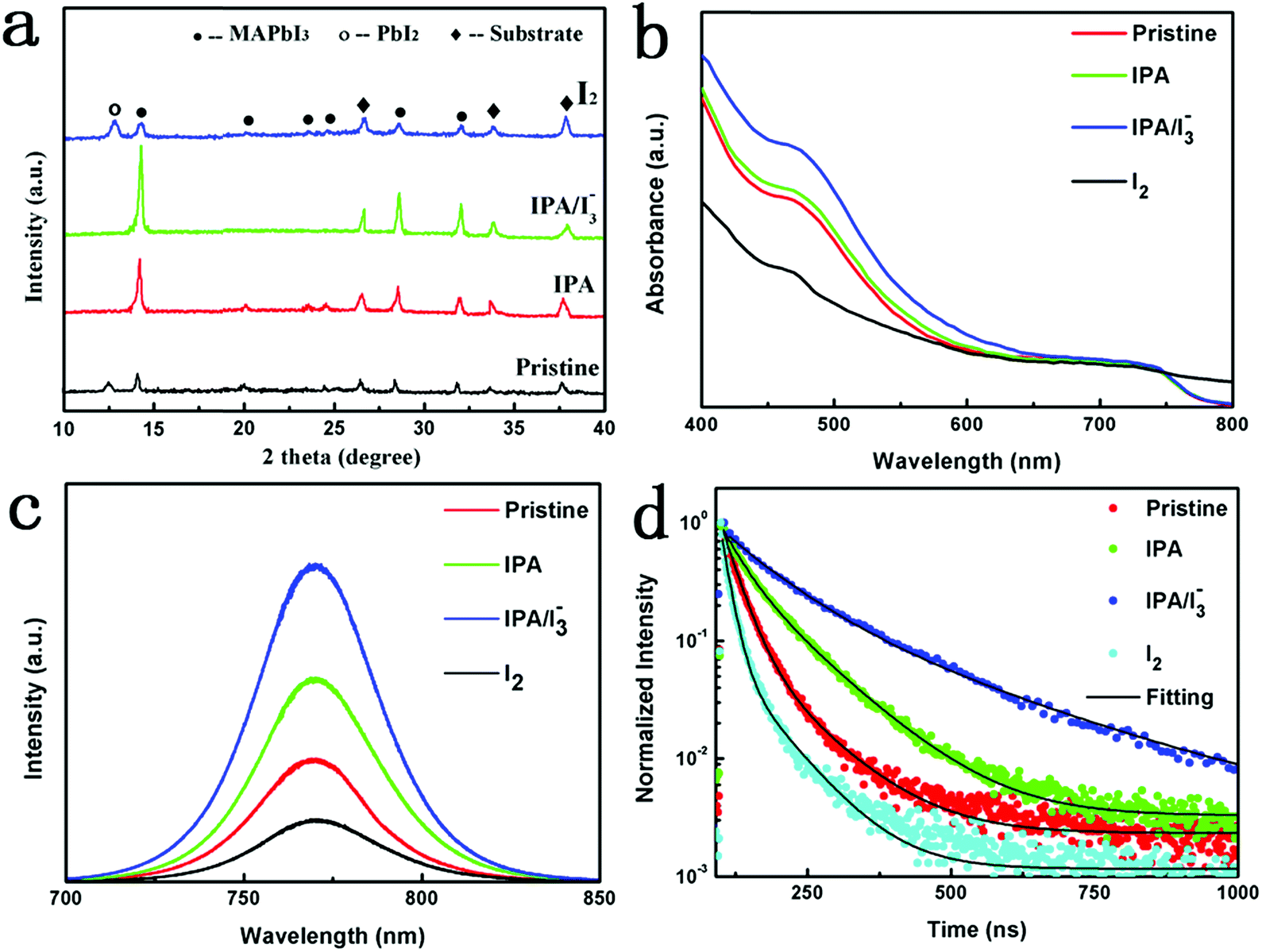 | ||
| Fig. 2 (a) XRD spectra, (b) UV-vis absorbance spectra, (c) steady-state photoluminescence (PL) spectra and (d) time-resolved photoluminescence (TRPL) spectra of perovskite films annealed by different approaches. | ||
UV-vis absorbance spectrum measurement was carried out to evaluate the effect of IPA/[I3−] vapor annealing on the optical properties of perovskite films. As seen in Fig. 2b, the IPA film shows an enhanced absorption compared with the pristine film. With further introduction of IPA/[I3−] vapor, the light absorption in the full range is significantly enhanced which is attributed to the improved quality of the perovskite film. However, when the film was annealed in pure I2 vapor, the absorption dramatically decreased and the absorption edge at 770 nm almost disappeared, suggesting that the film is degraded by the I2 vapor.47
To investigate the effect of IPA/[I3−] vapor annealing on the trap states of the perovskite films, we performed steady-state photoluminescence (PL) spectrum and time-resolved photoluminescence (TRPL) spectrum measurements. All samples were deposited on blank glass substrates to avoid the influence of charge injection in the electron transfer layer and perovskite light absorption layer. The steady-state PL spectra of the perovskite films with an excitation wavelength of 400 nm are compared in Fig. 2c. All the samples show a PL peak at 770 nm which is consistent with the results of UV-vis absorbance spectra. Compared with the pristine sample, the PL intensities of IPA and IPA/[I3−] samples are obviously enhanced, suggesting that the non-radiative recombination is dramatically suppressed.48 In particular, the PL intensity is enhanced by around 3 times after the introduction of [I3−] in the solvent vapor. To quantitatively analyze the dynamics of carrier recombination, we carried out TRPL spectrum measurement. And the PL decay curves monitored at the emission peak at 770 nm are fitted with a biexponential decay function:
Y = A1![[thin space (1/6-em)]](https://www.rsc.org/images/entities/char_2009.gif) exp(−t/τ1) + A2exp(−t/τ2) exp(−t/τ1) + A2exp(−t/τ2) | (3) |
Although the introduction of [I3−] into IPA vapor can improve the quality of the perovskite film, excessive [I3−] in the vapor will decrease the material's performance. We examined the effects of concentration on morphology, crystallinity, optical properties and photovoltaic performance. The FESEM images given in Fig. S3† show that a moderate amount of [I3−] in the IPA vapor does enlarge the grain size, and the grain size enlarged with the concentration of [I3−]. But cracks and pinholes are found when the added I2 concentration reaches 0.2%, which decreased the quality of the perovskite film. The XRD patterns in Fig. S4a† show that the intensity of the (110) diffraction peak at 14.2° increases with the concentration of [I3−], which demonstrates that the crystallinity is gradually increased. Furthermore, UV-vis absorbance and PL spectrum measurements show that the IPA/[I3−] vapor annealing with different [I3−] concentrations does not significantly change the band gap values, as seen in Fig. S4b and c.† And the optical performance increases with the [I3−] concentration when it is less than 0.15%, which is attributed to the improved surface morphology and reduced defect density. With further increase of [I3−] concentration, absorbance and PL emission performance are decreased due to the poor quality of the perovskite film. These results verify that a moderate amount of [I3−] in IPA vapor can reduce the defect density, but excessive [I3−] concentration in the vapor will decrease the quality of the perovskite film.
2.2 Photovoltaic performance
The current density–voltage (J–V) curves of PSCs based on perovskite films annealed in IPA vapor which contain different [I3−] concentrations were measured under one sun illumination. As shown in Fig. S5 and Table S2,† as the [I3−] concentration increases, the photovoltaic performance first increases, reaches a maximum value (the added I2 concentration is 0.15%), and then decreases. Therefore, the optimal [I3−] concentration is obtained when the added I2 concentration is 0.15%. To further investigate the effect of the IPA/[I3−] vapor annealing on the photovoltaic performance of PSCs, the J–V curves of the pristine, IPA and IPA/[I3−] devices were obtained and are compared in Fig. 4a, and the corresponding photovoltaic parameters are summarized in Table S3.† The pristine PSCs show a short circuit current density (Jsc) of 20.14 mA cm−2, open circuit voltage (Voc) of 1.00 V, fill factor (FF) of 0.70, and PCE of 14.16%. The inferior PCE of the pristine PSCs is mainly caused by the poor quality of the film, which results in charge recombination. When the IPA vapor is introduced into the annealing process, the PCE of the device is remarkably boosted. The J–V curve shows that the Jsc increases to 21.18 mA cm−2 with slightly improved Voc (1.03 V) and FF (0.72), which leads to an increased PCE of 15.61%. This is ascribed to the introduced IPA vapour which can retard the crystal formation and improve the quality of the perovskite film.41 Although the film quality is improved by the IPA vapor annealing, the ionic point defects induced by the under-coordinated Pb and I ions are not healed, which has been demonstrated by the XPS result in Fig. 6 and iodine vacancy defects in Scheme 1c. When the [I3−] is further introduced, the IPA/[I3−] device shows a significantly improved performance with a Jsc of 22.57 mA cm−2, Voc of 1.08 V, FF of 0.76, and PCE of 18.53%. This can be attributed to the reduced ionic point defects within the perovskite film, which are responsible for the formation of non-radiative recombination centers.9 In striking contrast, the device based on the perovskite film annealed in pure I2 vapor shows the worst performance with a PCE of 8.08%, even worse than that of the pristine PSCs. This is attributed to the fact that the charged ionic point defects cannot be healed by the charge-neutral I2 vapor, and even accelerate the degradation of perovskite films.25,52 In addition, the Jsc value obtained from J–V curves is well matched with the integrated current density obtained from the external quantum efficiency (EQE). The high EQE value of 93% for IPA/[I3−] PSCs throughout the entire wavelength range demonstrates a lower carrier recombination rate resulting from the reduced defect density. Moreover, the statistical PCE histogram of the devices along with the Gaussian fitting is shown in Fig. 3c. The IPA/[I3−] devices exhibit an excellent average PCE of 18% over 20 devices, which confirms the impressive reproducibility. | ||
| Fig. 3 (a) J–V curves (reverse scanning direction) and (b) EQE spectrum and integrated Jsc of devices based on perovskite films annealed by different approaches. (c) The statistics of PCE distribution for pristine, IPA and IPA/[I3−] devices (statistics from 20 samples for each vapor annealing process); the solid lines represent the Gaussian distribution fitting for the statistics of PCE. | ||
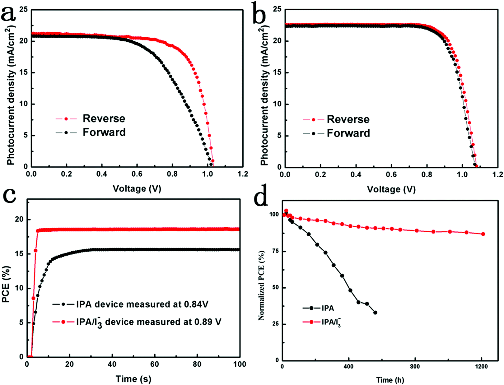 | ||
| Fig. 4 (a and b) J–V curves of the IPA and IPA/[I3−] devices, respectively, measured in both reverse (red) and forward (black) scanning directions. (c) The steady-state power output at the maximum power point for IPA and IPA/[I3−] devices, respectively. (d) Long-term stability of IPA and IPA/[I3−] devices (25 °C with a humidity of 10–20%), respectively. | ||
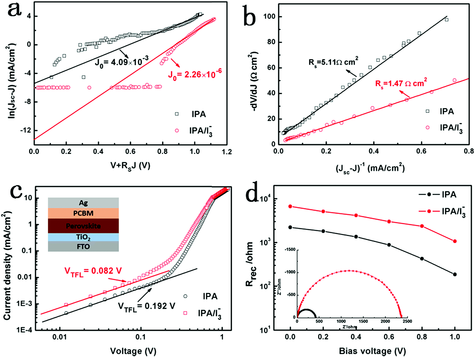 | ||
| Fig. 5 Plots of (a) ln(Jsc − J) vs. (V + RsJ) and (b) −dV/dJ vs. (Jsc − J)−1 with the linear fittings for the IPA and IPA/[I3−] devices, respectively. (c) Dark J–V curves from electron-only devices with the structure shown in the inset. (d) Recombination resistance (Rrec) of the IPA and IPA/[I3−] devices under different bias voltages. Inset: the Nyquist plots of the corresponding devices measured under dark conditions at a bias of 0.8 V. | ||
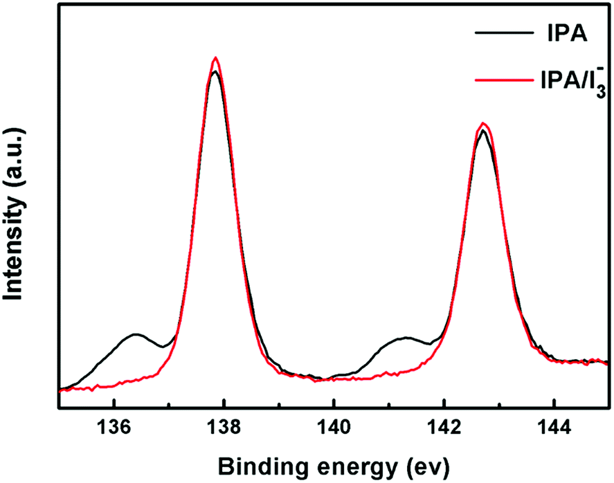 | ||
| Fig. 6 XPS spectra for Pb 4f from the IPA and IPA/[I3−] MAPbI3 films, respectively. | ||
Hysteresis is a critical issue in estimating the actual efficiency of devices, and thus the J–V curves are measured in both reverse scan (RS) and forward scan (FS) directions. In order to explore the function of [I3−], the following discussions are mainly focused on the comparison between the IPA device and the IPA/[I3−] device. As shown in Fig. 4a and b, the device based on the IPA perovskite film exhibits a severe J–V hysteresis (15%), while the J–V hysteresis is significantly suppressed (0.5%) after the introduction of [I3−] into the IPA solvent vapor. It has been reported that the hysteresis in different scan directions is mainly caused by ion migration originating from the defects in the perovskite layer.53 To further identify the suppressed hysteresis of the IPA/[I3−] device, the steady-state output of PCE is measured at constant bias voltages of the maximum power points, as shown in Fig. 4c. For the device based on the IPA/[I3−] perovskite film, it rapidly reached a stabilized power output of 18.50%, whereas the IPA device takes more time to reach steady state with a maximum power output of 15.58%. The results explicitly consolidate the suppressed hysteresis by the introduction of [I3−] during the IPA vapor annealing process.
Long-term stability is one of the most critical issues for the practical application of PSCs. To investigate the effect of IPA/[I3−] vapor annealing on the stability of PSCs, the devices based on IPA and IPA/[I3−] films were stored in an air environment under different conditions: 25 °C with a humidity of 10–20%, continuous AM 1.5 G illumination, a humidity of 50% and a temperature of 70 °C, respectively. Fig. 4d shows the normalized PCE as a function of storage time at 25 °C. Clearly, the IPA/[I3−] device shows excellent stability in the ambient environment. After 1200 h of storage, the IPA/[I3−] device retained 88% of its initial PCE, while that of the IPA device dropped to less than 40% after 500 h of storage. Moreover, the illumination stability, moisture stability and thermal stability are also enhanced after the introduction of [I3−] as shown in Fig. S7.† Consequently, the long-term stability is dramatically enhanced by the introduction of [I3−] during the IPA solvent vapor annealing process. According to a previous report, the degradation of the perovskite film generally starts at the defect sites such as iodine vacancies.34 Obviously, the superb stability is attributed to the decreased ionic point defects.
In order to further understand the improved photovoltaic performance of the IPA/[I3−] device, J–V curves are analyzed based on the single heterojunction solar cell theory.54,55 As shown in Fig. 5a and b, the reverse saturated current density (J0) and the series resistance (Rs) can be obtained from the intercepts of linear fitting of ln(Jsc − J) vs. (V + RsJ) and −dV/dJ vs. (Jsc − J)−1 plots, respectively. The calculated J0 values are 4.09 × 10⁻³ and 2.26 × 10⁻⁶ mA cm−2 for the IPA and IPA/[I3−] devices, respectively, while the corresponding Rs is 5.11 and 1.47 Ω cm2. Clearly, the improved photovoltaic performance is related to the decrease of J0 and Rs. J0 represents the thermal emission rate of electrons from the valence band to the conduction band in the light absorbing layer, which is directly proportional to the recombination rate of charge carriers. The decrease in Rs is a result of the more favorable charge transport in the IPA/[I3−] device. It is known that charge transport behavior benefits from the reduced trap states. Thus, the decreased J0 and Rs suggest the reduced trap states and the suppressed recombination of photo-generated carriers.
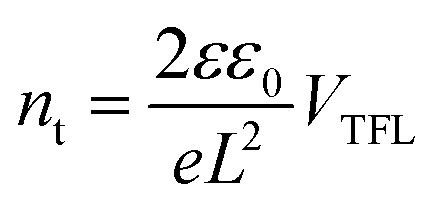
To quantitatively analyze the effect of IPA/[I3−] vapor annealing on the trap states, the electron trap state density is measured by the space-charge-limited current (SCLC) method. The electron-only cells with the architecture of FTO/TiO2/perovskite/PCBM/Ag are fabricated, and the corresponding dark J–V curves of the devices with IPA and IPA/[I3−] vapor annealing are compared in Fig. 5c. The J–V curves show a linear growth in current at low electric fields, suggesting an ohmic regime. When the applied bias voltage exceeds the kink point, the current shows a nonlinear increase, corresponding to a trap-filled limit region. Therefore, the bias voltage at the kink point is defined as the trap-filled limit voltage (VTFL) and the trap-state density (nt) can be described as
 | (4) |
To further elucidate the interfacial charge transport behavior under real cell working conditions, electrochemical impedance spectroscopy (EIS) measurement was carried out. The inset of Fig. 5d shows the Nyquist plots of the IPA and IPA/[I3−] devices under dark conditions at a reverse potential of 0.8 V. The equivalent circuit is provided in Fig. S8,† where Rs is the series resistance and Rrec is the recombination resistance. When the [I3−] is introduced into the IPA vapor, the Rrec extracted from the fitting results increased from 424 to 2360 Ω, indicating that trap-assisted recombination is suppressed in the IPA/[I3−] device. In addition, the derived Rrec values under various bias voltages are plotted in Fig. 5d. The Rrec of the IPA/[I3−] device is larger than that of the IPA device under the same bias voltage, which suggests an improved electron conductivity.
2.3 Possible mechanism of [I3−] induced performance improvement
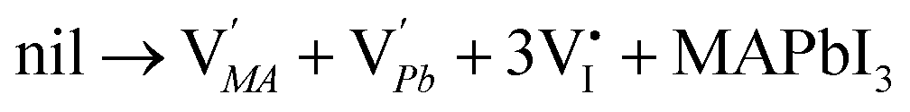
To analyse the mechanism of [I3−] induced performance improvement, X-ray photoelectron spectroscopy (XPS) measurement of MAPbI3 films was carried out to clarify the iodine vacancies before and after the introduction of [I3−]. The XPS results in Fig. 6 show the core level Pb 4f spectra. We observe two main peaks of Pb 4f7/2 and Pb 4f5/2 at 138.0 eV and 142.8 eV, respectively, which are consistent with previous reports.56 Moreover, the additional small peaks at 136.4 eV and 141.3 eV are attributed to the presence of metallic Pb.57 The result indicates that iodine vacancies exist in the perovskite lattice of the IPA sample surface. It suggests that the ionic point defects in the perovskite lattice are not healed by pure IPA vapor annealing. And the iodine vacancies may act as non-radiative recombination centers which decrease the performance of PSCs. It is intriguing that the atomic Pb peak is significantly reduced by the introduction of [I3−] during the IPA solvent vapor annealing process. This is attributed to the decreased iodine vacancies in the crystal lattice of the IPA/[I3−] perovskite film. The fewer ionic point defects lead to less non-radiative recombination and longer PL lifetime.To explore the role of [I3−] in improving the MAPbI3 film, the corresponding mechanism is discussed. For hybrid organic–inorganic halide perovskite materials, Schottky disorder is the dominant type of point defect. Considering full Schottky disorder, anion and cation vacancies are created and randomly distributed in MAPbI3 perovskite crystals as described in eqn (5) in the Kröger–Vink notation:58
 | (5) |
It well known that the solvent vapor annealing is a recrystallization process. During the recrystallization process, [I3−] ions in IPA vapor are incorporated into the MAPbI3 lattice, and thus the charged ionic point defects are healed by the negatively charged [I3−] ions. Specifically speaking, the positively charged  can be easily compensated for by the negatively charged [I3−] anion in the annealing vapor, leading to a perfect MAPbI3 lattice, as described in Scheme 1(c) and eqn (6):
 | (6) |
Therefore, the IPA solvent vapor which contains [I3−] would heal the ionic point defects and enhance the photovoltaic performance significantly.
Recent experimental studies have verified that the migration of I−and MA+ occurs within the lattice of MAPbI3 films when the elevated temperature is higher than 330 K.59–61 Therefore, the mobile ions in MAPbI3 films can be described as follows (eqn (7)) from the viewpoint of thermodynamic chemical potentials:
| CH3NH3PbI3 ⇌ PbI2 + I− + CH3NH3+ | (7) |
The excessive [I3−] in the vapor will decrease the corresponding performance. This can be attributed to the fact that the excessive [I3−] will react with the migrating CH3NH3+ ions, and thus decompose the film. The related equation can be described as follows:
| CH3NH3+ + I3− → CH3NH2 + I2 + HI | (8) |
When the MAPbI3 film is annealed by the charge-neutral I2 vapor, a set of chemical reactions take place. Under the thermal stress
| I2 → 2I˙ | (9) |
 | (10) |
 | (11) |
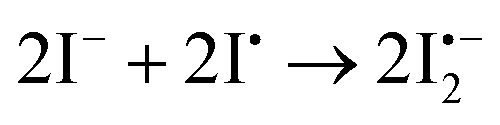
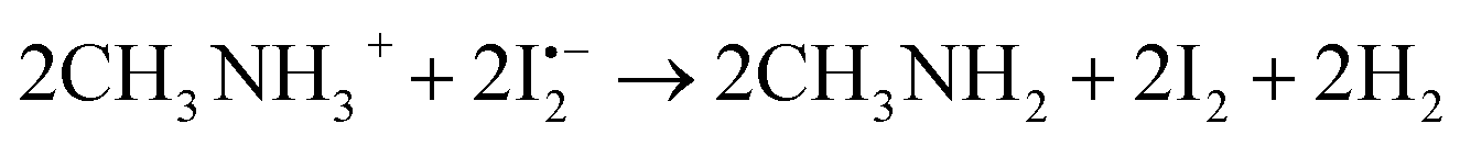
The atomic iodine (I˙) is generated from the thermolysis of I2 according to eqn (9); then the mobile I− in the MAPbI3 lattice will react with I˙, leading to the formation of  as described in eqn (10).62 The standard Gibbs free energy (ΔG) of eqn (11) is calculated to be −390.9 kJ mol−1, indicating that the chemical reaction from the left to the right is thermodynamically favourable. This indicates that
  can subsequently react with mobile CH3NH3+ ions as described in eqn (11). This suggests that I2 vapor annealing alone cannot heal the ionic point defects, and even accelerates the degradation of the perovskite film.25,52 These results indicate that negatively charged tri-iodide ions which have strong interaction with defects are favorable for the defect healing.
3. Conclusion
In summary, we adopt an ionic compensation strategy based on tri-iodide ions to heal ionic point defects during the solvent vapor annealing process. A high quality perovskite film with fewer ionic point defects is obtained by the IPA solvent vapor annealing and it contains tri-iodide ions. The PCE of the device fabricated with IPA/[I3−] vapor annealing shows an improvement of 30% compared with the pristine device and the best performing device achieves a PCE of 18.53%. Furthermore, with the introduction of [I3−] into the IPA vapor, the notorious J–V hysteresis almost disappears, and the long-term stability is significantly enhanced. This work represents an important direction toward realizing high performance PSCs. Moreover, we anticipate that the ionic compensation strategy can be applied to other photovoltaic devices such as photodetectors, photoelectric sensors and light-emitting diodes.4. Experimental section
The MAPbI3 films were fabricated by a two-step method based on the mesoporous TiO2 layer. The solvent vapor annealing process was carried out in a Petri dish filled with IPA vapor, IPA/[I3−] vapor or I2 vapor, respectively. All annealing processes were carried out on a hotplate at 100 °C for 60 min. A pristine MAPbI3 perovskite film without any solvent vapor was also prepared for contrast study. More experimental details are provided in the ESI.†Conflicts of interest
There are no conflicts to declare.Acknowledgements
This work was financially supported by the National Natural Science Foundation of China (No. 51272086) and the Technology Development Program of Jilin Province (Grant no. 20130206078GX).Notes and references
- D.-Y. Son, J.-W. Lee, Y. J. Choi, I.-H. Jang, S. Lee, P. J. Yoo, H. Shin, N. Ahn, M. Choi, D. Kim and N.-G. Park, Nat. Energy, 2016, 1, 16081 CrossRef CAS.
- M. He, X. Pang, X. Liu, B. Jiang, Y. He, H. Snaith and Z. Lin, Angew. Chem., Int. Ed. Engl., 2016, 55, 4280–4284 CrossRef CAS PubMed.
- J. Zhang, G. Zhai, W. Gao, C. Zhang, Z. Shao, F. Mei, J. Zhang, Y. Yang, X. Liu and B. Xu, J. Mater. Chem. A., 2017, 5, 4190–4198 RSC.
- X. Meng, X. Cui, M. Rager, S. Zhang, Z. Wang, J. Yu, Y. W. Harn, Z. Kang, B. K. Wagner, Y. Liu, C. Yu, J. Qiu and Z. Lin, Nano Energy, 2018, 52, 123–133 CrossRef CAS.
- M. Saliba, J. P. Correa-Baena, M. Gratzel, A. Hagfeldt and A. Abate, Angew. Chem., Int. Ed. Engl., 2018, 57, 2554–2569 CrossRef CAS PubMed.
- S. Wang, T. Sakurai, W. Wen and Y. Qi, Adv. Mater. Interfaces, 2018, 1800260 CrossRef.
- A. Kojima, K. Teshima, Y. Shirai and T. Miyasaka, J. Am. Chem. Soc., 2009, 131, 6050–6051 CrossRef CAS PubMed.
- H.-S. Kim, C.-R. Lee, J.-H. Im, K.-B. Lee, T. Moehl, A. Marchioro, S.-J. Moon, R. Humphry-Baker, J.-H. Yum, J. E. Moser, M. Graetzel and N.-G. Park, Sci. Rep., 2012, 2, 00591 CrossRef PubMed.
- W. S. Yang, B.-W. Park, E. H. Jung, N. J. Jeon, Y. C. Kim, D. U. Lee, S. S. Shin, J. Seo, E. K. Kim, J. H. Noh and S. I. Seok, Science, 2017, 356, 1376–1379 CrossRef CAS PubMed.
- Best Research Cell Efciences, (NREL, accessed Aug, 27th, 2018), https://www.nrel.gov/pv/assets/images/efficiencychart.png.
- M. He, B. Li, X. Cui, B. Jiang, Y. He, Y. Chen, D. O'Neil, P. Szymanski, M. A. Ei-Sayed, J. Huang and Z. Lin, Nat. Commun., 2017, 8, 16045 CrossRef CAS PubMed.
- M. He, D. Zheng, M. Wang, C. Lin and Z. Lin, J. Mater. Chem. A., 2014, 2, 5994–6003 RSC.
- H. J. Snaith, A. J. Moule, C. Klein, K. Meerholz, R. H. Friend and M. Gratzel, Nano Lett., 2007, 7, 3372–3376 CrossRef CAS PubMed.
- D. Bi, W. Tress, M. I. Dar, P. Gao, J. Luo, C. Renevier, K. Schenk, A. Abate, F. Giordano, J.-P. C. Baena, J.-D. Decoppet, S. M. Zakeeruddin, M. K. Nazeeruddin, M. Gratzel and A. Hagfeldt, Sci. Adv., 2016, 2, 1501170 CrossRef PubMed.
- F. Cai, Y. Yan, J. Yao, P. Wang, H. Wang, R. S. Gurney, D. Liu and T. Wang, Adv. Funct. Mater., 2018, 28, 1801985 CrossRef.
- G. Yang, C. Wang, H. Lei, X. Zheng, P. Qin, L. Xiong, X. Zhao, Y. Yan and G. Fang, J. Mater. Chem. A., 2017, 5, 1658–1666 RSC.
- M. Ye, C. He, J. Iocozzia, X. Liu, X. Cui, X. Meng, M. Rager, X. Hong, X. Liu and Z. Lin, J. Phys. D: Appl. Phys., 2017, 50, 373002 CrossRef.
- D. Shi, V. Adinolfi, R. Comin, M. Yuan, E. Alarousu, A. Buin, Y. Chen, S. Hoogland, A. Rothenberger, K. Katsiev, Y. Losovyj, X. Zhang, P. A. Dowben, O. F. Mohammed, E. H. Sargent and O. M. Bakr, Science, 2015, 347, 519–522 CrossRef CAS PubMed.
- W.-J. Yin, T. Shi and Y. Yan, Appl. Phys. Lett., 2014, 104, 063903 CrossRef.
- A. Buin, P. Pietsch, J. Xu, O. Voznyy, A. H. Ip, R. Comin and E. H. Sargent, Nano Lett., 2014, 14, 6281–6286 CrossRef CAS PubMed.
- A. Buin, R. Comin, J. Xu, A. H. Ip and E. H. Sargent, Chem. Mater., 2015, 27, 4405–4412 CrossRef CAS.
- B. Conings, J. Drijkoningen, N. Gauquelin, A. Babayigit, J. D'Haen, L. D'Olieslaeger, A. Ethirajan, J. Verbeeck, J. Manca, E. Mosconi, F. De Angelis and H.-G. Boyen, Adv. Energy Mater., 2015, 5, 1500477 CrossRef.
- L. Hu, T. Liu, L. Sun, S. Xiong, F. Qin, X. Jiang, Y. Jiang and Y. Zhou, Chem. Commun., 2018, 54, 4704–4707 RSC.
- S. Xiao, Y. Bai, X. Meng, T. Zhang, H. Chen, X. Zheng, C. Hu, Y. Qu and S. Yang, Adv. Funct. Mater., 2017, 27, 1604944 CrossRef.
- S. Wang, Y. Jiang, E. J. Juarez-Perez, L. K. Ono and Y. Qi, Nat. Energy, 2016, 2, 16195 CrossRef.
- X. Zhu, J. Lee and W. D. Lu, Adv. Mater., 2017, 29, 1700527 CrossRef PubMed.
- J. Cao, X. Jing, J. Yan, C. Hu, R. Chen, J. Yin, J. Li and N. Zheng, J. Am. Chem. Soc., 2016, 138, 9919–9926 CrossRef CAS PubMed.
- M. Abdi-Jalebi, Z. Andaji-Garmaroudi, S. Cacovich, C. Stavrakas, B. Philippe, J. M. Richter, M. Alsari, E. P. Booker, E. M. Hutter, A. J. Pearson, S. Lilliu, T. J. Savenije, H. Rensmo, G. Divitini, C. Ducati, R. H. Friend and S. D. Stranks, Nature, 2018, 555, 497–501 CrossRef CAS PubMed.
- J. Kim, S.-H. Lee, J. H. Lee and K.-H. Hong, J. Phys. Chem. Lett., 2014, 5, 1312–1317 CrossRef CAS PubMed.
- M. L. Agiorgousis, Y.-Y. Sun, H. Zeng and S. Zhang, J. Am. Chem. Soc., 2014, 136, 14570–14575 CrossRef CAS PubMed.
- M. M. Byranvand, S. Song, L. Pyeon, G. Kang, G.-Y. Lee and T. Park, Nano Energy, 2017, 34, 181–187 CrossRef CAS.
- Y. Shao, Y. Yuan and J. Huang, Nat. Energy, 2016, 1, 15001 CrossRef CAS.
- X. Zheng, B. Chen, J. Dai, Y. Fang, Y. Bai, Y. Lin, H. Wei, X. C. Zeng and J. Huang, Nat. Energy, 2017, 2, 17102 CrossRef CAS.
- Q. Wang, B. Chen, Y. Liu, Y. Deng, Y. Bai, Q. Dong and J. Huang, Energy Environ. Sci., 2017, 10, 516–522 RSC.
- A. G. Aberle, Prog. Photovoltaics, 2000, 8, 473–487 CAS.
- A. Neumuller, O. Sergeev, S. J. Heise, S. Bereznev, O. Volobujeva, J. F. L. Salas, M. Vehse and C. Agert, Nano Energy, 2018, 43, 228–235 CrossRef.
- J. Xu, A. Buin, A. H. Ip, W. Li, O. Voznyy, R. Comin, M. Yuan, S. Jeon, Z. Ning, J. J. McDowell, P. Kanjanaboos, J. P. Sun, X. Lan, L. N. Quan, D. H. Kim, I. G. Hill, P. Maksymovych and E. H. Sargent, Nat. Commun., 2015, 6, 7081 CrossRef CAS PubMed.
- N. K. Noel, A. Abate, S. D. Stranks, E. S. Parrott, V. M. Burlakov, A. Goriely and H. J. Snaith, ACS Nano, 2014, 8, 9815–9821 CrossRef CAS PubMed.
- A. Manglik, S. K. Sharma and V. P. Kudesia, React. Kinet. Catal. Lett., 1981, 15, 467–473 CrossRef.
- J. M. Gardner, M. Abrahamsson, B. H. Farnum and G. J. Meyer, J. Am. Chem. Soc., 2009, 131, 16206–16214 CrossRef CAS PubMed.
- X. Sun, C. Zhang, J. Chang, H. Yang, H. Xi, G. Lu, D. Chen, Z. Lin, X. Lu, J. Zhang and Y. Hao, Nano Energy, 2016, 28, 417–425 CrossRef CAS.
- D. Liu, M. K. Gangishetty and T. L. Kelly, J. Mater. Chem. A., 2014, 2, 19873–19881 RSC.
- C. Fei, B. Li, R. Zhang, H. Fu, J. Tian and G. Cao, Adv. Energy Mater., 2017, 7, 1602017 CrossRef.
- W. Zhu, L. Kang, T. Yu, B. Lv, Y. Wang, X. Chen, X. Wang, Y. Zhou and Z. Zou, Appl. Mater. interfaces, 2017, 9, 6104–6113 CrossRef CAS PubMed.
- J. T.-W. Wang, Z. Wang, S. Pathak, W. Zhang, D. W. deQuilettes, F. Wisnivesky-Rocca-Rivarola, J. Huang, P. K. Nayak, J. B. Patel, H. A. Mohd Yusof, Y. Vaynzof, R. Zhu, I. Ramirez, J. Zhang, C. Ducati, C. Grovenor, M. B. Johnston, D. S. Ginger, R. J. Nicholas and H. J. Snaith, Energy Environ. Sci., 2016, 9, 2892–2901 RSC.
- S. Y. Leblebici, L. Leppert, Y. Li, S. E. Reyes-Lillo, S. Wickenburg, E. Wong, J. Lee, M. Melli, D. Ziegler, D. K. Angell, D. F. Ogletree, P. D. Ashby, F. M. Toma, J. B. Neaton, I. D. Sharp and A. Weber-Bargioni, Nat. Energy, 2016, 1, 16093 CrossRef CAS.
- J. A. Christians, P. A. Miranda Herrera and P. V. Kamat, J. Am. Chem. Soc., 2015, 137, 1530–1538 CrossRef CAS PubMed.
- W. Zhou, P. Zhou, X. Lei, Z. Fang, M. Zhang, Q. Liu, T. Chen, H. Zeng, L. Ding, J. Zhu, S. Dai and S. Yang, Appl. Mater. interfaces, 2018, 10, 1897–1908 CrossRef CAS PubMed.
- J. Jin, H. Li, C. Chen, B. Zhang, L. Xu, B. Dong, H. Song and Q. Dai, Appl. Mater. interfaces, 2017, 42875–42882 CrossRef CAS PubMed.
- A.-N. Cho, N. Chakravarthi, K. Kranthiraja, S. S. Reddy, H.-S. Kim, S.-H. Jin and N.-G. Park, J. Mater. Chem. A., 2017, 5, 7603–7611 RSC.
- L. M. Herz, Annu. Rev. Phys. Chem., 2016, 67, 65–89 CrossRef CAS PubMed.
- L. Zhang and P. H. L. Sit, J. Mater. Chem. A., 2017, 5, 23976–23986 RSC.
- X. Liu, Y. Zhang, L. Shi, Z. Liu, J. Huang, J. S. Yun, Y. Zeng, A. Pu, K. Sun, Z. Hameiri, J. A. Stride, J. Seidel, M. A. Green and X. Hao, Adv. Energy Mater., 2018, 8, 1800138 CrossRef.
- J. Shi, J. Dong, S. Lv, Y. Xu, L. Zhu, J. Xiao, X. Xu, H. Wu, D. Li, Y. Luo and Q. Meng, Appl. Phys. Lett., 2014, 104, 063901 CrossRef.
- J. You, Y. Yang, Z. Hong, T.-B. Song, L. Meng, Y. Liu, C. Jiang, H. Zhou, W.-H. Chang, G. Li and Y. Yang, Appl. Phys. Lett., 2014, 105, 183902 CrossRef.
- C. Das, M. Wussler, T. Hellmann, T. Mayer and W. Jaegermann, Phys. Chem. Chem. Phys., 2018, 20, 17180–17187 RSC.
- D. Bi, C. Yi, J. Luo, J.-D. Décoppet, F. Zhang, S. M. Zakeeruddin, X. Li, A. Hagfeldt and M. Grätzel, Nat. Energy, 2016, 1, 16142 CrossRef CAS.
- A. Walsh, D. O. Scanlon, S. Chen, X. G. Gong and S.-H. Wei, Angew. Chem., Int. Ed., 2015, 54, 1791–1794 CrossRef CAS PubMed.
- C. Eames, J. M. Frost, P. R. F. Barnes, B. C. O'Regan, A. Walsh and M. S. Islam, Nat. Commun., 2015, 6, 8497 CrossRef PubMed.
- Y. Yuan, Q. Wang, Y. Shao, H. Lu, T. Li, A. Gruverman and J. Huang, Adv. Energy Mater., 2016, 6, 1501803 CrossRef.
- A. M. A. Leguy, J. M. Frost, A. P. McMahon, V. G. Sakai, W. Kockelmann, C. Law, X. Li, F. Foglia, A. Walsh, B. C. O'Regan, J. Nelson, J. T. Cabral and P. R. F. Barnes, Nat. Commun., 2015, 6, 8124 CrossRef PubMed.
- L. Wan and Y. Xu, Photochem. Photobiol. Sci., 2013, 12, 2084–2088 RSC.
Footnote |
| † Electronic supplementary information (ESI) available. See DOI: 10.1039/c8ta10094b |
| This journal is © The Royal Society of Chemistry 2019 |