
 Open Access Article
 This Open Access Article is licensed under a
 Creative Commons Attribution 3.0 Unported Licence
Operando electrochemical study of charge carrier processes in water splitting photoanodes protected by atomic layer deposited TiO2†
Wei
Cui
 a,
Thomas
Moehl
a,
Sebastian
Siol
b and
S. David
Tilley
*a
a,
Thomas
Moehl
a,
Sebastian
Siol
b and
S. David
Tilley
*a
aDepartment of Chemistry, University of Zurich, Winterthurerstrasse 190, CH-8057 Zurich, Switzerland. E-mail: david.tilley@chem.uzh.ch
bEmpa – Swiss Federal Laboratories for Materials Science and Technology, Überlandstrasse 129, CH-8600 Dübendorf, Switzerland
First published on 3rd September 2019
Abstract
Semiconductor-based solar energy conversion devices are often multilayer structures with each layer serving a distinct purpose towards generating an efficient and stable device. In water splitting, the use of atomic layer deposited TiO2 (ALD-TiO2) layers enables the stable operation of materials that would normally photocorrode in the aqueous electrolyte. Interestingly, thick ALD-TiO2 (>50 nm) has been successfully used to protect high performance photoanodes, despite an apparent band mismatch that should preclude charge transfer. The understanding of the charge transfer through the relatively thick TiO2 layer remains controversial and warrants further study. Here, we introduce an operando methodology to study charge carrier processes in the ALD-TiO2 protected photoanode by utilizing photoelectrochemical impedance spectroscopy (PEIS) combined with the dual-working-electrode (DWE) technique to resolve if the charge transport through the TiO2 is a conduction band process or involves a hopping through defect states. Two silicon-based systems were evaluated, one featuring a buried homojunction (np+Si/TiO2/Ni) and the other a purely n-type Si directly interfaced with TiO2 (nSi/TiO2/Ni). The additional series resistance imparted by the TiO2 layer (RTiO2) was extracted from the PEIS measurements. Both the potential and thickness dependence of RTiO2 were analyzed, and the DWE technique enabled the sensing of the potential of the TiO2 layer under operation, indicating a strong band bending with the conduction band even more positive than the oxygen evolution potential. Together, these data suggest a conduction band-based transport mechanism, in spite of the presence of defect states in the bandgap of ALD-TiO2, and a detailed picture of the charge transfer through the multilayer structured photoanodes was obtained.
Introduction
Solar to hydrogen conversion by photoelectrochemical (PEC) water splitting has been recognized as a promising approach to meet the growing demand of sustainable energy. In PEC systems, a photoelectrode utilizes a semiconductor/electrolyte interface and simultaneously functions as a light harvesting unit as well as an electrocatalyst.1,2 To date, tremendous effort has been put into fabricating photoelectrodes in a multilayer configuration to enhance both the efficiency and stability.3 For example, silicon (Si), the most successful material in solar energy conversion, exhibits poor stability and an unfavorable catalytic activity for water splitting. To address this, surface electrocatalysts have been applied, such as CoPi4 and Ni5 for O2 evolution, and Pt6 and MoSx7 for H2 evolution. To further stabilize Si, additional protective layers have been introduced, including thin metals, oxides and ultrathin insulator layers.8,9 Amongst all protective layers, TiO2 produced by atomic layer deposition (ALD) is especially attractive, considering the conformal morphology, robust chemical stability and optical properties showing transparency in the visible part of the electromagnetic spectrum.10,11 Moreover, the electrical conductivity of TiO2 enables unimpeded charge transport through the protective layer of H2-evolving photocathodes.12Interestingly, ALD-TiO2 has also been shown to protect nSi-based photoanodes, demonstrating hole transport through the TiO2, which is a seeming contradiction considering its n-type conductivity arising from oxygen vacancies. Nevertheless, the photo-excited holes are transported through the TiO2, arriving at the water oxidation catalyst on the surface where the oxidative reaction takes place. For an ultrathin TiO2 layer (<2 nm), a direct tunneling mechanism was proposed by McIntyre and co-workers, as depicted in Scheme S1a.†4,13 This tunneling mechanism is also operative with other ultrathin insulators such as Al2O3 and SiO2,14 however, it is not able to explain the hole transfer through a thicker TiO2 layer. Hu et al. proposed a mechanism where holes can be transported through a band of defect states deep in the bandgap of the TiO2 (Scheme S1b†).15,16 Mei et al., however, demonstrated that crystalline TiO2 can also be used as a protection layer for photoanodes (Scheme S1c†).17 It should be noted that in contrast to the Hu et al. study, Mei et al. fabricated the TiO2 by reactive sputtering, and a Ti metal layer at the interface of the Si and TiO2 ensured an ohmic contact. We sought to clarify whether such a conduction band mechanism is also operative in ALD-TiO2 protected photoanodes in the absence of the Ti metal layer. Due to the high complexity of these multilayered devices, in-depth investigation of charge carrier processes is still challenging, which limits further optimization of the system. Therefore, it is highly desirable to develop an operando methodology that can provide high spatial and temporal charge dynamics of the underlying charge transfer processes during PEC operation.18,19
Photoelectrochemical impedance spectroscopy (PEIS) is an established method for characterizing charge carrier phenomena under operational conditions. It has been commonly employed to detect the origin of limitations and improve the efficiency of these solar energy conversion devices.20,21 The impedance response of the system is usually displayed in a Nyquist plot, where charge carrier processes can be visualized and distinguished by the semicircle features in different frequency domains. For a complex multilayer photoelectrode system with so far unknown equivalent circuit (EC), still the resistances of the different charge carrier processes can be extracted and their potential dependence studied.22,23
The dual-working-electrode (DWE) technique is another powerful tool to study fundamental insights of water splitting photoelectrodes. While the first working electrode (WE1) controls the potential at the back contact of the photoelectrode, the second working electrode (WE2) contacts either the catalyst on the surface or the photoabsorber surface itself, thereby enabling the in situ monitoring of, or control of, the surface potential. Thus, junction behaviors can be directly revealed. For example, the Boettcher group applied the DWE technique to study semiconductor/catalyst junctions and the semiconductor degradation mechanism in O2-evolving photoanodes.24,25
Here, we report a systematic study to elucidate the detailed charge carrier processes in ALD-TiO2 protected photoanodes by using the PEIS and DWE techniques. Two Si-based systems were investigated, namely np+Si/TiO2/Ni and nSi/TiO2/Ni photoanodes. We carefully studied the “hole-leaky” property of the TiO2 by analyzing the corresponding resistance (RTiO2). Both the potential and thickness dependence of RTiO2 was analyzed and the RTiO2 features from an np+Si/TiO2/Ni photoanode as well as a pn+Si/TiO2/Pt photocathode were compared. A conduction band transport mechanism agrees well with the experimental results, despite the presence of defect states in the bandgap. Additionally, we adopted the DWE technique to study the interface energetics of the ALD-TiO2 protected photoanodes. The second working electrode, connected to the TiO2 or p+Si layer, was used both as an in situ probe of the surface potential as well as controlling the surface potential during PEIS measurements. By this means, a systematic investigation of the charge carrier processes in ALD-TiO2 protected photoanodes can be achieved. Finally, the different behaviors of charge transfer at the p+Si/TiO2 and nSi/TiO2 interface is discussed, elucidating the influence of the defect states in ALD-TiO2.
Results and discussion
R TiO2 in np+Si/TiO2/Ni photoanode
The efficiency of an np+Si/TiO2/Ni photoanode is largely determined by the intrinsic properties of the buried np+ junction. Additionally, the electrochemical properties of the TiO2 protection layer play a crucial role for the overall water oxidation performance. Band alignment and positions, including the Fermi level position of each involved layer, are helpful for analyzing and predicting charge carrier processes under illumination in these structures. Fig. 1a provides the band alignments of nSi, p+Si and ALD-TiO2 layers (the process by which the alignment was determined is found in the ESI†). Note that the TiO2 is highly n-type doped and both the Fermi level and CB are energetically situated close to E(H+/H2), which makes TiO2 an ideal material as a protective layer for photocathodes.12 Defect states inside the ALD-TiO2 layer, located around the thermodynamic water oxidation potential, E(H2O/O2), were confirmed by X-ray photoelectron spectroscopy (XPS) measurements (Fig. S2†).15,26 From the band alignment in Fig. 1, we note several observations. First, hole transfer through the TiO2 valence band is highly unlikely due to the large VB offset between Si and TiO2. Second, the defect states situated around E(H2O/O2) could be a pathway for hole transfer through the TiO2 layer, which is the model proposed by Hu et al.15 Third, p+Si/TiO2 may form an ohmic contact due to the high doping density for both of them, i.e. the space-charge regions in both materials at this junction will be thin enough such that charges can easily tunnel through. This mechanism would be similar to the model by Mei et al. whereby the charges are transported in the conduction band of TiO2 (with strong band bending at the TiO2/electrolyte interface such that the potential is positive enough to enable water oxidation).17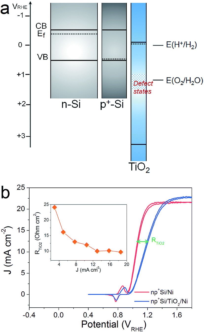 | ||
| Fig. 1 (a) Band structures of nSi, p+Si and ALD-TiO2 before contact. CB and VB are the energetic positions of the conduction band and valence band of a semiconductor, respectively, shown by solid lines. Ef is the Fermi level, indicated with dashed lines. (b) Typical CVs of np+Si/Ni photoanodes with or without 100 nm thick TiO2 protective layer in 1 M KOH under one sun illumination. The fill factor (FF) difference results from the increased series resistance brought by the TiO2 layer (RTiO2). The inset shows RTiO2 as a function of photocurrent density calculated from the J–V curves. | ||
We hypothesized that it should be possible to distinguish between the conduction band model and the defect-state model by analyzing the potential-dependent resistances of the TiO2 layer and interfaces. Fig. 1b presents typical cyclic voltammograms (CVs) of np+Si/Ni photoanodes with and without 100 nm ALD-TiO2 layer in 1 M KOH (aq) under one sun illumination. A clear fill factor (FF) decrease can be observed for the TiO2 protected one, indicating that the TiO2 layer indeed introduces an extra series resistance (RTiO2). Approximate RTiO2 values were calculated through a simple method: in the photocurrent-rising potential region (1.0–1.2 VRHE), the potential difference of the two JV curves in Fig. 1b was divided by the photocurrent density. The inset of Fig. 1b plots RTiO2 values versus the photocurrent density, exhibiting a reduction of RTiO2 as the current increases (the reason for which is discussed below). The slightly higher saturation current density from np+Si/TiO2/Ni can be attributed to sample to sample variation (see also Fig. S7†).
As the presence of RTiO2 has been confirmed, we can now develop a picture of the charge carrier processes in an np+Si/TiO2/Ni photoanode under water oxidation conditions. As illustrated in Fig. 2a, we consider three main processes. When illuminated, minority carrier (holes) are excited and move to the p+Si/TiO2 interface by the built-in electric field across the np+Si homojunction, accompanied by a charge recombination process either in the bulk of Si or the space charge region (process 1 in Fig. 2a). Process 2 represents that charge carriers somehow transfer through the thick ALD-TiO2 layer and arrive at the Ni catalyst. This process contains clues to the understanding about the “hole-leaky” properties of TiO2. The third process is the charge transfer at the catalyst surface for water oxidation, which of course requires a potential in excess of the thermodynamic potential for oxygen evolution. These three steps can be expressed in terms of resistances obtained from the impedance measurements. The EC model used for fittings is provided in Fig. 2a, wherein all resistances are in series. We note that even though several EC models have been developed to describe PEC processes, it is the capacitive rather than resistive elements which distinguish them.23 This is why our following analysis is fully resistance-based. The fitting details are presented in Fig. S3.† Clear multi-semicircle features and voltage-dependency can be observed. Fig. 2b plots the typical J–V curve of a np+Si/TiO2/Ni photoanode, as well as the voltage-dependent values of the resistances obtained from the fit of the measured impedance spectra.
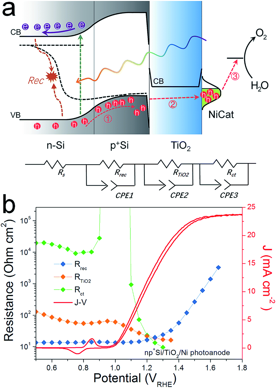 | ||
| Fig. 2 (a) Schematic illustration of charge transfer processes and the energy band alignment of an O2-evolving np+Si/TiO2/Ni photoanode. The depicted process 1 represents the recombination taking place inside the buried np homojunction; process 2 represents the charge transfer through the TiO2 protective layer to reach the surface Ni catalyst (NiCat); process 3 represents the water oxidation reaction process on the NiCat. The model used for fitting the EIS data is illustrated as well. Rs is the series resistance from the electrolyte solution. Rrec, RTiO2 and Rct are assigned to process 1, 2, and 3, respectively. (b) Resistances and photocurrent densities (J) versus the back contact potential. Rrec, RTiO2 and Rct were obtained from fittings of Nyquist plots. Rs was not plotted here. | ||
The high frequency resistance, Rrec, shows a low and constant value in the pre-onset potential region and exponentially increases after the onset potential. Generally, Rrec represents the overall recombination processes taking place in the space charge region and the bulk of the absorber, with larger values being better for device performance. The small Rrec values before the onset potential imply that the charge cannot be injected into the electrolyte solution and thus can only recombine. After passing the onset potential, charges can flow into the electrolyte solution, the recombination process is reduced due to the efficient charge separation, and under increased bias, Rrec consequently increases.
The low frequency resistance, Rct, has large values (104 ohm cm2) before the onset potential, representing the inhibited O2-evolving charge transfer process over the Ni catalyst into the electrolyte solution. Notably, Rct shows a valley in the Ni-redox potential region, indicating the increased current flow due to the catalyst oxidation (0.9–1.1 VRHE). Afterwards, the resistance increases again before it steeply drops as the overpotential of NiCat is overcome and oxygen evolution current sets in.23,27 As the O2-involving photocurrent increases, the value of Rct drastically reduces and finally disappears at very positive potential region (after 1.4 VRHE), suggesting fast charge transfer kinetics at the catalyst/electrolyte interface.
R TiO2, with an intermediate frequency range, is related to the charge carrier processes in the TiO2 protective layer. We note that several sub-process resistances can contribute to the overall RTiO2, including charge transfer through the Si/TiO2 and TiO2/Ni catalyst interfaces, as well as the charge transport inside the TiO2 layer. In the potential window from 0.4 to 1.3 VRHE, RTiO2 declines and shows a valley in the Ni-redox potential region. This valley is due to the hole storing properties of the NiCat. Both the downward trend and values of RTiO2 in the potential region of >1.0 VRHE are consistent with the results shown in the inset of Fig. 1b, providing further evidence for the correct assignment of this process to the TiO2 layer. Additionally, we performed V2-controlled impedance measurements under illumination, wherein the p+Si Fermi level was controlled by the second working electrode, as shown in Fig. S4–S6.† In this case, RTiO2 was also observed and shows similar potential dependence to that in V1-controlled measurements. Notably, RTiO2 shows a shift between the V1 and V2 controlled impedance spectra (Fig. 3a), which arises from the photovoltage provided by the underlying PV. The defect states mediated hole transport in amorphous TiO2 is assumed to be based on a hopping transport mechanism, occurring in filled defect states (Ti3+) related to O vacancies and other impurities such as N and C species.26 The hole hopping rate strongly depends on the distance between Ti3+ sites.28 Compared to electron transport in the conduction band, the hole hopping rate inside the defect band should be much slower and therefore show an increased resistivity.28,29 Thus, we hypothesized that RTiO2 ought to exhibit a thickness dependence if the defect states mechanism were operative. We therefore studied the charge transport in the TiO2 protective layer by varying the thickness of the TiO2 layer in the range of 50 to 170 nm. Fig. S7† shows that thicker TiO2 does not lead to a significantly decreased FF in the J–V curve. Fig. 3b exhibits a similar potential dependence of RTiO2 extracted from these samples, and RTiO2 values do not show a clear thickness dependence over the whole potential range, which is indicative of a transport through the conduction band.
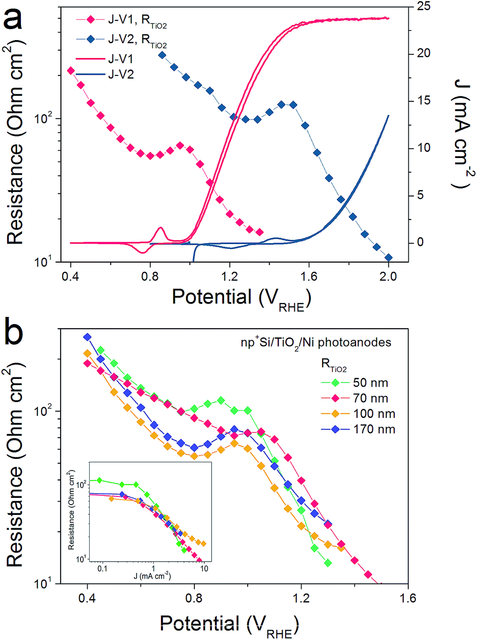 | ||
| Fig. 3 (a) RTiO2 obtained from back contact potential (V1) and front contact potential (V2) controlled measurements. (b) RTiO2 thickness dependence. Inset is the RTiO2 as a function of the photocurrent density. | ||
For comparison, a pn+Si/TiO2/Pt photocathode system was investigated, where electron transport in the conduction band of TiO2 is not controversial (Fig. 4). Similarly, three charge carrier processes are presented in Fig. 4a, in accordance with the Nyquist and Bode plots shown in Fig. S8.† As can be seen in Fig. 4b, Rct shows large values until the hydrogen-evolving current rises, and then quickly disappears. Also, Rrec shows small values before the onset of H2 evolution, and increases as the photocurrent current increases under increasingly strong bias (inhibiting recombination). RTiO2 decreases upon scanning to more negative potentials, from thousands to a few ohm cm2, and eventually disappears. RTiO2 also appears in V2-controlled PEIS measurements and exhibits a photovoltage-shift (Fig. 4c), similarly to the photoanode case. As compared to the photoanodes, the thickness independence of RTiO2 is apparent in Fig. 4d. The observed features of RTiO2 show clear similarity with those in the np+Si/TiO2/Ni photoanode system, which is again an indication for the conduction band mechanism of the “hole-leaky” TiO2 in the photoanode, even though the defect states in TiO2 are present.
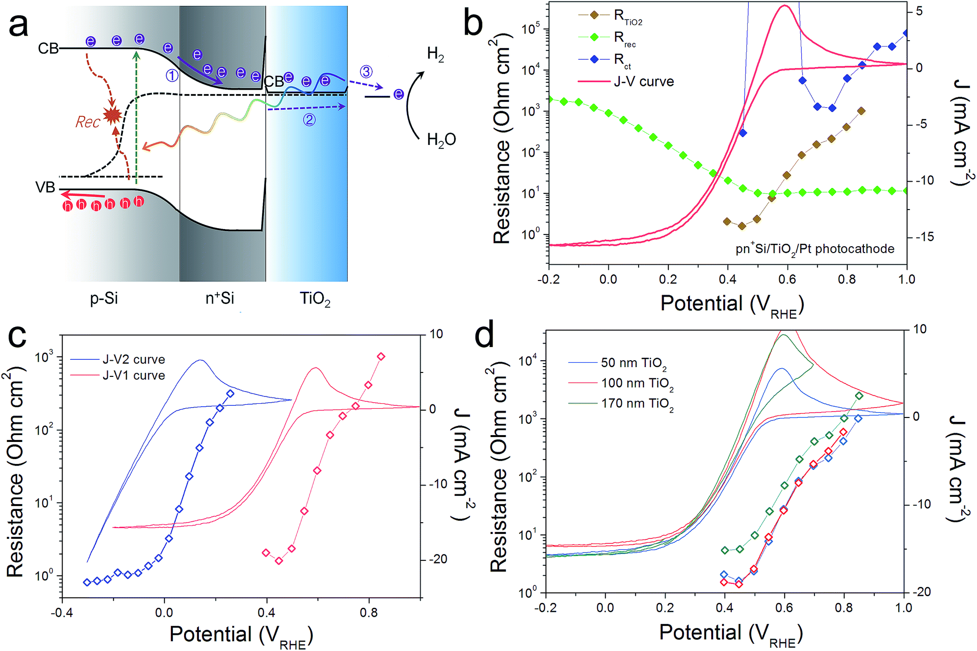 | ||
| Fig. 4 (a) Schematic energy band alignment in a H2-evolving pn+Si/TiO2/Pt photocathode. Similarly, the depicted process 1 represents the recombination taking place inside the buried pn+ homojunction; process 2 represents the charge transfer through the TiO2 protective layer and to reach the surface Pt catalyst; process 3 represents the hydrogen evolution reaction process on the Pt. (b) Resistances and photocurrent densities versus the back contact potential. (c) RTiO2 obtained from V1 and V2 controlled. (d) CVs and RTiO2 values measured from pn+Si/TiO2/Pt photocathodes with different TiO2 thickness. | ||
Electron transfer at the p+Si/TiO2 and TiO2/Ni interfaces
Above we studied the charge transport inside the TiO2 layer, where a conduction band mechanism has been proposed to interpret the “hole-leaky” property of TiO2. In the following, we analyse the charge transfer across the interfaces. Two interfaces are involved for the np+Si/TiO2/Ni configuration, p+Si/TiO2 and TiO2/NiCat. The DWE technique, allowing in situ surface potential sensing, was applied to study the interface properties. A stepwise chronoamperometric measurement was carried out whereby the potential of V1, equal to Ef(nSi), stepped towards more positive potential, and both the front contact V2 and the photocurrent were simultaneously recorded. V2 was equal to either the Ef(p+Si) in an np+Si/Ni photoanode or the Ef(TiO2) in an np+Si/TiO2/Ni photoanode. As can be observed in Fig. 5a, Ef(TiO2) and Ef(p+Si) exhibit almost the same trend except for slight deviation (∼50 mV).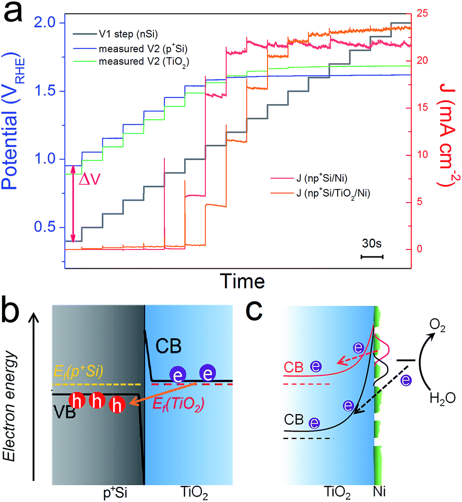 | ||
| Fig. 5 (a) Ef(p+Si) and J values of np+Si/Ni; Ef(TiO2) and J values of np+Si/TiO2/Ni photoanode with stepwise controlled V1 Ef(nSi) under one sun illumination. Each V1 step lasts 30 s. Band diagrams and charge transfer processes at (b) p+Si/TiO2 and (c) TiO2/NiCat/electrolyte interfaces. Due to the high doping density in both p+Si and TiO2, the depletion regions in (b and c) are very narrow, in the range of a few nm.17 | ||
The change of V2 with respect to the V1 potential is typical of a buried junction photoelectrode, reported in our previous work.30 At less positive V1, such as 0.5 or 0.6 VRHE, V2 is not positive enough to drive water oxidation. ΔV values remain constant and equal to Voc. As soon as V2 is slightly more positive than the E(O2/H2O) (note that the overpotential of the NiCat must be accounted for), water oxidation is thermodynamically allowed, and electrons flow from the electrolyte/NiCat into the TiO2 layer, accompanied by the generation of O2 gas. The ΔV value begins to shrink as the O2-evolving photocurrent increases and the Ef to the electrolyte is pinned by the redox potential of the O2 evolution reaction. The moment V1 reaches the same value as V2, the buried np+ junction is at the short-circuit condition. Finally, as the photocurrent becomes saturated due to the photon flux and recombination limitation, V2 reaches a steady value independent of V1. The reverse bias across the np+ junction becomes stronger as the controlled V1 level increases to more positive potentials.
Fig. S9† depicts the architecture of the electrode as well as the band diagram at the contact of the second working electrode. This surface contact is remote from the actual voltage generating part of the photocathode and covered with thick epoxy (∼1 mm from the active area and effectively in the dark, even while illuminating the active area), and is simply sensing the potential V2 with no current flow, implying a standard equilibration of the Fermi levels across the Si/TiO2/Au interfaces. As no holes could be sustained in the defect band under this open-circuit condition, WE2 is sensing the Fermi level of the electrons (the majority carriers) in the TiO2, which is situated very close to the conduction band edge due to the high donor density. Equilibrium of the TiO2 with the underlying p+Si is then attained via band bending. Both p+Si and TiO2 layers are highly doped, and as a result, the space charge region in the junction is narrow enough for efficient electron tunneling (Fig. 5b). In such a situation, there is nearly no barrier for electrons entering p+Si valence band from the TiO2 conduction band.
As is evident from Fig. 5a, the conduction band of TiO2 becomes even more positive than the thermodynamic water oxidation potential. The onset potential for the O2 evolution of the np+Si/TiO2/Ni photoanode is around 1.1 VRHE, when Ef(TiO2) is 1.6 VRHE. Notably, 1.6 VRHE is also the onset potential of the J–V2 curve in Fig. 3a. The transition from an effective open circuit condition (at potentials where V2 is not positive enough to oxidize water) to potentials where water oxidation occurs shows a smooth trend of the TiO2 Fermi level, analogous to the photocathode case,30 and a transport through defect states need not be invoked. Our observations are in accordance with the description of the conduction band mechanism by Mei et al., where the electrons are generated from the water oxidation process.17 Electrons cannot enter the TiO2 conduction band until the barrier of TiO2/electrolyte and catalyst overpotential are overcome, as drawn in Fig. 5c. This is also true for photocathodes. The barrier of TiO2/electrolyte must be overcome first, then electrons can enter the electrolyte solution and reduce protons. However, RTiO2 exhibits very different values in the prior-to-onset potential region for the photoanode and photocathode. Generally, under operational conditions, the RTiO2 is lower for the photocathode case since we expect a lower barrier to the electrolyte (see Fig. S10†). On the other hand, in the photocathode case, RTiO2 varies from nearly 103 ohm cm2 in the prior-to-onset potential range, while in the photoanode case, RTiO2 only shows 100 ohm cm2 in the near-zero current region. This suggests that the electron transfer still occurs across the TiO2 layer even in the prior-to-onset potential. We attribute this phenomenon to the ion-permeable property of NiCat. Many researchers have demonstrated that NiCat plays a role of so-called “hole-collector” as the catalyst in photoanode.31,32 Holes are first collected and oxidize NiCat. When the NiCat energy level is sufficiently positive, holes enter the electrolyte solution and oxidize water to oxygen. Similarly, in the np+Si/TiO2/Ni photoanode, in the prior-to-onset potential region, electrons from NiCat enter TiO2 conduction band and NiCat is oxidized, resulting in nearly zero net photocurrent. When photocurrent rises, electrons generated by water oxidation process enter TiO2 conduction band (Fig. 5c). In comparison, Pt is not ion-permeable and no electrons can transfer into the TiO2 and be collected in Pt catalyst until cathodic photocurrent rises, which is why RTiO2 shows extremely high values in the prior-to-onset potential region in the pn+Si/TiO2/Pt photocathode. Moreover, it is important to note that the morphology of the NiCat plays a crucial role in the solid/liquid interface.24 The NiCat in our work deposited by sputtering was nominally 2 nm-thick, however, the layer is neither conformal nor continuous and has an island morphology, as confirmed by scanning electron microscopy (SEM) and atomic force microscopy (AFM) (Fig. S11 and S12†). Thus, the TiO2 directly contacts the electrolyte solution, which pins the band edge of the TiO2. In the presence of the Ni catalyst and at high applied bias (large band bending), electrons from the electrolyte solution are thus able to tunnel through the narrow depletion region and enter the TiO2 conduction band due to the high doping density of TiO2.12
R TiO2 in nSi/TiO2/Ni photoanode
The conduction band mechanism has been implicated with the np+S/TiO2/Ni photoanode system in the above discussion. Next, we wished to study the charge transfer across a non-homojunction system, the nSi/TiO2/Ni photoanode, wherein the nSi/TiO2 interface is significantly different to the p+Si/TiO2 interface. In the nSi/TiO2/Ni photoanode, the nSi/TiO2 interface cannot be seen as an ohmic contact due to the non-degenerate nSi. A photovoltage of 90 mV was measured by the DWE technique (Fig. S13†). The buried junction behaviour of nSi/TiO2 interface was demonstrated by the stepwise DWE measurements results. As can be seen in Fig. S14,† ΔV keeps a value of 85 mV in the prior-to-onset potential region. With photocurrent rising, ΔV starts to shrink. Ef(TiO2) becomes constant as the photocurrent becomes saturated. A built-in voltage (Vbi) of 320 mV was measured with the Mott–Schottky method (Fig. S15†). We note that both the photovoltage and built-in voltage are smaller compared to the values in Hu et al.'s work, which are 390 and 700 mV, respectively.33 This considerable difference can arise from the different experimental procedure. In our system, the TiO2 layer was immediately deposited after the HF-etching in order to avoid the formation of surface SiO2 formation. In Hu et al.'s work, the HF-etched Si wafers were subsequently immersed in H2O/HCl/H2O2 solution (RCA-2 Treatments), which made the oxide layer regrow.34,35 Presumably, this ultrathin SiO2 layer either passivates surface states or unpins nSi so that larger photovoltage can be achieved. Nevertheless, this difference to previous work does not affect the following analysis.PEIS measurements for the nSi/TiO2/Ni photoanode were carried out under 0.1 sun illumination to increase the signal to noise ratio. Fitting details can be found in Fig. S16.† Similarly, Rrec, RTiO2 and Rct were extracted. Fig. 6a presents the CV of the nSi/TiO2/Ni photoanode as well as the voltage-dependent values of Rrec, RTiO2 and Rct. Due to the limited Vph generated by nSi/TiO2, a much later onset potential (1.5 VRHE) was observed than for the np+Si/TiO2/Ni junction. Rrec values are low and constant and continue to increase as the photocurrent rises. Rct mirrors the CV, exhibiting large values that rapidly decrease after onset potential. Fig. 6b shows that the thickness of the TiO2 layer does not affect the fill factor of the J–V curve. RTiO2 does not show a thickness dependence, suggesting that the conduction band mechanism is also true in the nSi/TiO2/Ni photoanode system.
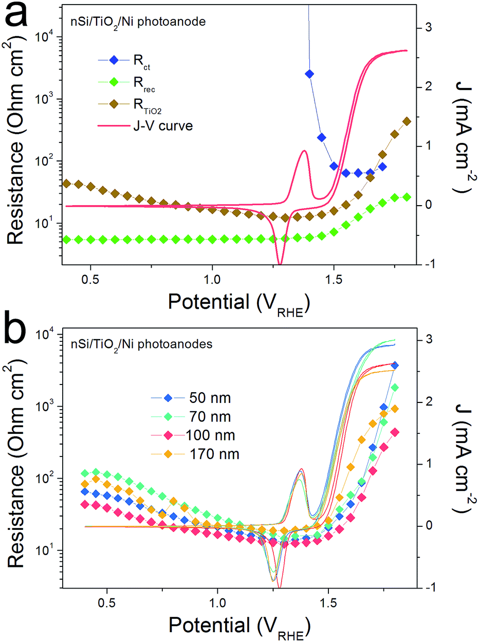 | ||
| Fig. 6 (a) Resistances and photocurrent densities (J) versus the back contact potential for a nSi/TiO2/Ni photoanode. (b) CVs and RTiO2 values measured from nSi/TiO2/Ni photoanodes with different TiO2 thickness. | ||
However, unlike the downward trend in np+Si/TiO2/Ni and pn+Si/TiO2/Pt, RTiO2 in nSi/TiO2/Ni shows a significant increase as photocurrent increases. This indicates a hidden process that hinders the charge transfer across the nSi/TiO2 interface. We attribute this limitation to the defect states in TiO2. Since Ef(TiO2) becomes constant, as shown in the above stepwise DWE measurements, the reverse bias between nSi and TiO2 is increasingly stronger. As illustrated in Fig. 7, when the Si Fermi level is more positive than the TiO2 defect states, electrons from the TiO2 conduction band can be trapped before entering the Si valence band. One possible trapping mechanism is that electrons at the TiO2 conduction band need to fill the empty trap states before entering Si valence band (i.e. before recombining with photo-excited holes in the nSi valence band). This trapping effect is growingly significant as the Ef(nSi) moves down, leading to slower charge kinetics and increased RTiO2 values.
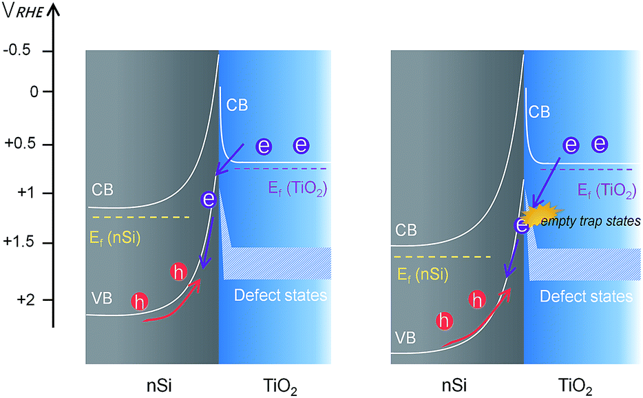 | ||
| Fig. 7 Band diagram and charge transfer process at the nSi/TiO2 interface with photogenerated holes. The doping density of nSi is much smaller so that the depletion region width in nSi is very large compared to that in TiO2 (in the range of hundreds of nm), resulting in a rectifying junction. | ||
Conclusions
In summary, we utilized PEIS and DWE techniques to systematically study the charge carrier processes in ALD-protected photoanodes. With PEIS measurements, the RTiO2 was assigned to represent the overall charge transfer through the TiO2 layer. For both RTiO2 np+Si/TiO2/Ni and nSi/TiO2/Ni photoanodes, RTiO2 did not show a clear thickness dependence, and the energetic position of the conduction band during operation as detected by the DWE technique suggests that the “hole-leaky” property of TiO2 can be explained by charge transport in the conduction band, in spite of the presence of the defect states in TiO2. RTiO2 behaved differently in the np+Si/TiO2/Ni and nSi/TiO2/Ni photoanode. In the np+Si/TiO2/Ni photoanode, RTiO2 showed a reduction/decrease over the whole potential range as the p+Si/TiO2 interface behaves like an ohmic junction. In the nSi/TiO2/Ni photoanode, RTiO2 increased as the photocurrent increases, which was interpreted by trapping in the defect states present at the interface of the nSi/TiO2.Finally, we demonstrated that even though the structural and electrical properties of TiO2 are highly dependent on the preparation method, the analysis methodology we provided here is universal. Moreover, as the multilayer structured and tandem junction solar to fuel devices rapidly grow, the in-depth investigation of charge carrier processes in PEC devices is meeting formidable challenges. Various in situ approaches have been developed, mostly utilizing spectroscopic and scanning-probe techniques such as synchrotron-based X-ray techniques and atomic force microscopy.36,37 Unfortunately, they often require costly and sophisticated equipment as well as idealized or reduced device structures, and they rarely provide comprehensive mechanistic information of PEC water splitting under realistic operational condition.38 Considering this, our operando analysis provides a less costly methodology and possesses a huge potential for deep and comprehensive study of the charge dynamics in future PEC process research.
Author contributions
W. C. and S. D. T. conceived the project, directed the experiments and analyzed the data. T. Moehl assisted with PEIS and AFM measurements. S. S. assisted with the XPS measurements. All authors contributed to data analysis, read and commented on the manuscript.Conflicts of interest
The authors declare no competing financial interest.Acknowledgements
The University of Zurich, the University Research Priority Program (URPP) LightChEC, and the Swiss National Science Foundation (AP Energy Grant # PYAPP2 160586) are gratefully acknowledged for financial support.References
- Z. Zhang and J. T. Yates, Chem. Rev., 2012, 112, 5520–5551 CrossRef CAS PubMed.
- M. G. Walter, E. L. Warren, J. R. McKone, S. W. Boettcher, Q. X. Mi, E. A. Santori and N. S. Lewis, Chem. Rev., 2010, 110, 6446–6473 CrossRef CAS PubMed.
- Y. He, T. Hamann and D. Wang, Chem. Soc. Rev., 2019, 48, 2182–2215 RSC.
- A. G. Scheuermann, J. D. Prange, M. Gunji, C. E. D. Chidsey and P. C. McIntyre, Energy Environ. Sci., 2013, 6, 2487–2496 RSC.
- M. F. Lichterman, S. Hu, M. H. Richter, E. J. Crumlin, S. Axnanda, M. Favaro, W. Drisdell, Z. Hussain, T. Mayer, B. S. Brunschwig, N. S. Lewis, Z. Liu and H. J. Lewerenz, Energy Environ. Sci., 2015, 8, 2409–2416 RSC.
- L. Ji, M. D. Mcdaniel, S. Wang, A. B. Posadas, X. Li, H. Huang, J. C. Lee, A. A. Demkov, A. J. Bard, J. G. Ekerdt and E. T. Yu, Nat. Nanotechnol., 2015, 10, 84–90 CrossRef CAS PubMed.
- B. Seger, A. B. Laursen, P. C. K. Vesborg, T. Pedersen, O. Hansen, S. Dahl and I. Chorkendorff, Angew. Chem., Int. Ed. Engl., 2012, 51, 9128–9131 CrossRef CAS PubMed.
- K. Sun, M. T. McDowell, A. C. Nielander, S. Hu, M. R. Shaner, F. Yang, B. S. Brunschwig and N. S. Lewis, J. Phys. Chem. Lett., 2015, 6, 592–598 CrossRef CAS PubMed.
- D. Bae, B. Seger, P. C. K. Vesborg, O. Hansen and I. Chorkendorff, Chem. Soc. Rev., 2017, 46, 1933–1954 RSC.
- A. G. Scheuermann and P. C. McIntyre, J. Phys. Chem. Lett., 2016, 7, 2867–2878 CrossRef CAS PubMed.
- M. F. Lichterman, K. Sun, S. Hu, X. Zhou, M. T. McDowell, M. R. Shaner, M. H. Richter, E. J. Crumlin, A. I. Carim, F. H. Saadi, B. S. Brunschwig and N. S. Lewis, Catal. Today, 2016, 262, 11–23 CrossRef CAS.
- B. Seger, T. Pedersen, A. B. Laursen, P. C. K. Vesborg, O. Hansen and I. Chorkendorff, J. Am. Chem. Soc., 2013, 135, 1057–1064 CrossRef CAS PubMed.
- Y. W. Chen, J. D. Prange, S. Dühnen, Y. Park, M. Gunji, C. E. D. Chidsey and P. C. McIntyre, Nat. Mater., 2011, 10, 539–544 CrossRef CAS PubMed.
- I. A. Digdaya, B. J. Trześniewski, G. W. P. Adhyaksa, E. C. Garnett and W. A. Smith, J. Phys. Chem. C, 2018, 122, 5462–5471 CrossRef CAS PubMed.
- S. Hu, M. R. Shaner, J. A. Beardslee, M. Lichterman, B. S. Brunschwig and N. S. Lewis, Science, 2014, 344, 1005–1009 CrossRef CAS PubMed.
- M. T. McDowell, M. F. Lichterman, A. I. Carim, R. Liu, S. Hu, B. S. Brunschwig and N. S. Lewis, ACS Appl. Mater. Interfaces, 2015, 7, 15189–15199 CrossRef CAS PubMed.
- B. Mei, T. Pedersen, P. Malacrida, D. Bae, R. Frydendal, O. Hansen, P. C. K. Vesborg, B. Seger and I. Chorkendorff, J. Phys. Chem. C, 2015, 119, 15019–15027 CrossRef CAS.
- C. Jiang, S. J. A. Moniz, A. Wang, T. Zhang and J. Tang, Chem. Soc. Rev., 2017, 46, 4645–4660 RSC.
- S. D. Tilley, Adv. Energy Mater., 2019, 9, 1802877 CrossRef.
- B. Klahr, S. Gimenez, F. Fabregat-Santiago, J. Bisquert and T. W. Hamann, J. Am. Chem. Soc., 2012, 134, 16693–16700 CrossRef CAS PubMed.
- L. Bertoluzzi, P. Lopez-Varo, J. A. Jiménez Tejada and J. Bisquert, J. Mater. Chem. A, 2016, 4, 2873–2879 RSC.
- D. Klotz, D. S. Ellis, H. Dotan and A. Rothschild, Phys. Chem. Chem. Phys., 2016, 18, 23438–23457 RSC.
- T. Moehl, W. Cui, R. Wick-Joliat and S. D. Tilley, Sustainable Energy Fuels, 2019, 3, 2067–2075 RSC.
- F. Lin and S. W. Boettcher, Nat. Mater., 2014, 13, 81–86 CrossRef CAS PubMed.
- F. A. L. Laskowski, M. R. Nellist, R. Venkatkarthick and S. W. Boettcher, Energy Environ. Sci., 2017, 10, 570–579 RSC.
- T. Moehl, J. Suh, L. Sévery, R. Wick-Joliat and S. D. Tilley, ACS Appl. Mater. Interfaces, 2017, 9, 43614–43622 CrossRef CAS PubMed.
- J. E. Thorne, J. W. Jang, E. Y. Liu and D. Wang, Chem. Sci., 2016, 7, 3347–3354 RSC.
- H. H. Pham and L. W. Wang, Phys. Chem. Chem. Phys., 2015, 17, 541–550 RSC.
- N. A. Deskins, J. Du and P. Rao, Phys. Chem. Chem. Phys., 2017, 19, 18671–18684 RSC.
- W. Cui, W. Niu, R. Wick-Joliat, T. Moehl and S. D. Tilley, Chem. Sci., 2018, 9, 6062–6067 RSC.
- F. A. L. Laskowski, M. R. Nellist, J. Qiu and S. W. Boettcher, J. Am. Chem. Soc., 2019, 141, 1394–1405 CrossRef CAS PubMed.
- C. Cui, M. Heggen, W. D. Zabka, W. Cui, J. Osterwalder, B. Probst and R. Alberto, Nat. Commun., 2017, 8, 1314 CrossRef PubMed.
- S. Hu, M. H. Richter, M. F. Lichterman, J. Beardslee, T. Mayer, B. S. Brunschwig and N. S. Lewis, J. Phys. Chem. C, 2016, 120, 3117–3129 CrossRef CAS.
- I. A. Digdaya, G. W. P. Adhyaksa, B. J. Trześniewski, E. C. Garnett and W. A. Smith, Nat. Commun., 2017, 8, 15968 CrossRef CAS PubMed.
- P. Nunez, M. H. Richter, B. D. Piercy, C. W. Roske, M. Cabán-Acevedo, M. D. Losego, S. J. Konezny, D. J. Fermin, S. Hu, B. S. Brunschwig and N. S. Lewis, J. Phys. Chem. C, 2019, 123, 20116–20129 CrossRef CAS.
- F. A. L. L. Laskowski, K. Sivula, H. Hajibabaei, M. R. Nellist, T. W. Hamann, J. Qiu, S. W. Boettcher, F. A. L. L. Laskowski, J. Qiu, H. Hajibabaei, K. Sivula, T. W. Hamann and S. W. Boettcher, Nat. Energy, 2017, 3, 46–52 Search PubMed.
- M. Plaza, X. Huang, J. Y. P. Ko, M. Shen, B. H. Simpson, J. Rodríguez-López, N. L. Ritzert, K. Letchworth-Weaver, D. Gunceler, D. G. Schlom, T. A. Arias, J. D. Brock and H. D. Abruña, J. Am. Chem. Soc., 2016, 138, 7816–7819 CrossRef CAS PubMed.
- J. Cen, Q. Wu, M. Liu and A. Orlov, Green Energy Environ, 2017, 2, 100–111 CrossRef.
Footnote |
| † Electronic supplementary information (ESI) available: Experimental details, Nyquist plots fitting and so on. See DOI: 10.1039/c9se00399a |
| This journal is © The Royal Society of Chemistry 2019 |