
Growing high-quality CsPbBr3 by using porous CsPb2Br5 as an intermediate: a promising light absorber in carbon-based perovskite solar cells†
Jiaming
Liu
a,
Liqun
Zhu
a,
Sisi
Xiang
a,
Ya
Wei
a,
Minling
Xie
b,
Huicong
Liu
a,
Weiping
Li
a and
Haining
Chen
 *a
*a
aSchool of Materials Science and Engineering, Beihang University, No. 37 Xueyuan Road, Haidian District, Beijing 100191, People's Republic of China. E-mail: chenhaining@buaa.edu.cn
bWuhan Second Ship Design and Research Institute, Wuhan 430064, Hubei, People's Republic of China
First published on 22nd October 2018
Abstract
CsPbBr3 with a large band gap (∼2.3 eV) is a promising material for fabricating perovskite solar cells (PSCs) with a high open-circuit voltage (Voc) and high stability. However, a suitable method is still lacking for depositing high-quality CsPbBr3 films. Herein, we develop a novel strategy to deposit high-quality CsPbBr3 films by employing a porous CsPb2Br5 film as an intermediate layer. Highly porous CsPb2Br5 films composed of lamellar crystals were obtained by immersing Pb–Br precursor layers in a low-concentration CsBr IPA solution. The low CsBr concentration helped to widen the processing window of CsPb2Br5, while the low-polarity IPA solvent served to keep the film structure stable during the reaction. High-quality CsPbBr3 films with full coverage, high purity and low defect density were obtained by further converting the CsPb2Br5 films in a high-concentration CsBr solution. After introducing the optimized CsPbBr3 film into a carbon-based PSC without a hole transporting material (C-PSC), a power conversion efficiency (PCE) of 6.1% and a Voc of 1.38 V were achieved. Moreover, the devices without encapsulation show almost no PCE decay after 200 days of storage in ambient air (25–85% relative humidity, 20–30 °C) and at 80 °C (10–20% relative humidity) for over 1080 h.
Introduction
Impressive progress has been made for organometal trihalide perovskite solar cells (PSCs) during the past few years, from the first reported power conversion efficiency (PCE) of 3.8% to over 23%.1–8 However, the presence of the organic components (MA+, FA+, etc.) in perovskite films and the utilization of expensive and operationally unstable organic hole transport materials (HTMs, e.g. spiro-OMeTAD) seriously affect the stability of the devices, which limits the applications of PSCs.9–13 In our previous work, we have solved these problems by using all-inorganic perovskites (CsPbBr3 and CsPbI3) as light absorbers and replacing the HTM and Au electrode with carbon electrodes.14–16 Compared with conventional PSCs, these carbon-based PSCs (C-PSCs) with inorganic perovskites exhibit improved device stability.17–19Among different inorganic perovskites, CsPbBr3 is a promising one because of its large bandgap (CsPbBr3 ∼ 2.3 eV) leading to high open-circuit voltage (Voc) and higher stability in ambient air.20,21 Therefore, C-PSCs based on CsPbBr3 show great prospects. So far, a number of methods have been employed to prepare CsPbBr3 layers for PSCs and the two-step method is the most common one, which involves the initial deposition of a Pb–Br precursor layer, followed by a conversion reaction in CsBr solution.19,22–26 However, the commonly used Pb–Br precursor layers are compact, which prohibits the diffusion of CsBr solution and hence limits the conversion of the precursor to CsPbBr3.14,24
Herein, we introduce a porous CsPb2Br5 intermediate layer as a precursor for the deposition of CsPbBr3 layers. The porous CsPb2Br5 intermediate was obtained by reaction between a Pb–Br layer and a low-concentration CsBr solution (1.7 mg ml−1). The use of isopropanol (IPA) as the solvent for the low-concentration CsBr solution allowed the fabrication of a highly porous CsPb2Br5 intermediate layer. A high-quality CsPbBr3 film was obtained by converting the porous CsPb2Br5 intermediate layer in a high-concentration CsBr solution (17 mg ml−1). The C-PSC based on the optimized CsPbBr3 film achieved a PCE of 6.1% with a high Voc of 1.38 V. Significantly, the non-encapsulated devices showed almost no PCE decay after storage in ambient air (25–85% relative humidity (RH), 20–30 °C) for 200 days and after storage in air at 80 °C (10–20% RH) for 1080 h.
Results and discussion
Fig. 1 shows the whole deposition procedure of the CsPbBr3 layer by employing CsPb2Br5 layers as intermediates. Firstly, the original Pb–Br precursor film was deposited on a mesoporous TiO2 layer by spin-coating using a 1.4 M PbBr2 solution in a mixed solvent of dimethylformamide/dimethyl sulfoxide (DMF/DMSO). As is well-known, DMSO exhibits excellent solubility with PbX2 (X = I, Br, Cl) and strong coordination with Pb2+.4,27–29 In addition, the high boiling point and low volatility of DMSO contribute to obtaining a stable liquid film at room temperature.30 To first form the CsPb2Br5 intermediate, it is important to create a circumstance with excess Pb–Br precursor. Hence, different from the traditional two-step method with a high CsBr concentration (e.g. higher than 10 mg ml−1), a low-concentration CsBr solution (1.7 mg ml−1) was used as the reaction solution. After the formation of CsPb2Br5, the sample was further converted to CsPbBr3 in a high-concentration CsBr solution (17 mg ml−1). The low-concentration CsBr solution contributes to significantly slowing down the conversion of the Pb–Br precursor to CsPbBr3, which widens the processing window of CsPb2Br5. During the conversion process of the Pb–Br precursor to CsPb2Br5, we found that the solvent of the low-concentration CsBr solution has a great effect on the morphology of the CsPb2Br5 films. Therefore, two typical solvents (isopropanol (IPA) and methanol) were chosen for this solution, and it is indicated that IPA is more suitable for growing high-quality CsPb2Br5 and CsPbBr3 films.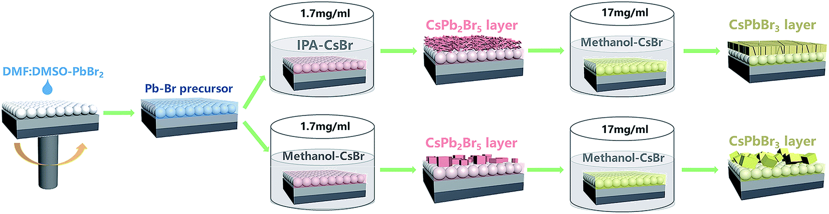 | ||
| Fig. 1 Schematic illustration of the deposition processes of CsPbBr3 films. | ||
Although the CsPb2Br5 films fabricated from IPA (I-CsPb2Br5) and methanol solutions (M-CsPb2Br5) have a similar appearance, the SEM images in Fig. 2a and b show quite different morphologies. The I-CsPb2Br5 film has a highly porous lamellar structure. This would enable much easier diffusion of the subsequent high-concentration (17 mg ml−1) CsBr methanol solution into the inner part of the layer and achieve efficient reaction between the CsPb2Br5 intermediate and CsBr. Small, fragmented and mutually overlapping crystals fully cover the mesoporous TiO2 layer. In comparison, the M-CsPb2Br5 film shows poor surface coverage. The relatively large crystals (∼1 μm) sparsely cover the substrate and a large area of the mesoporous TiO2 is exposed. The XRD patterns in Fig. 2c indicate that I-CsPb2Br5 and M-CsPb2Br5 exhibit similar phase structures and crystalline orientations. The intense diffraction peaks at 11.7°, 18.8°, 23.4°, 29.4° and 47.9° can be indexed to the (002), (112), (210), (213) and (420) planes of the CsPb2Br5 phase (PDF#25-0211), respectively, suggesting that the main component of the porous intermediate layer is CsPb2Br5.
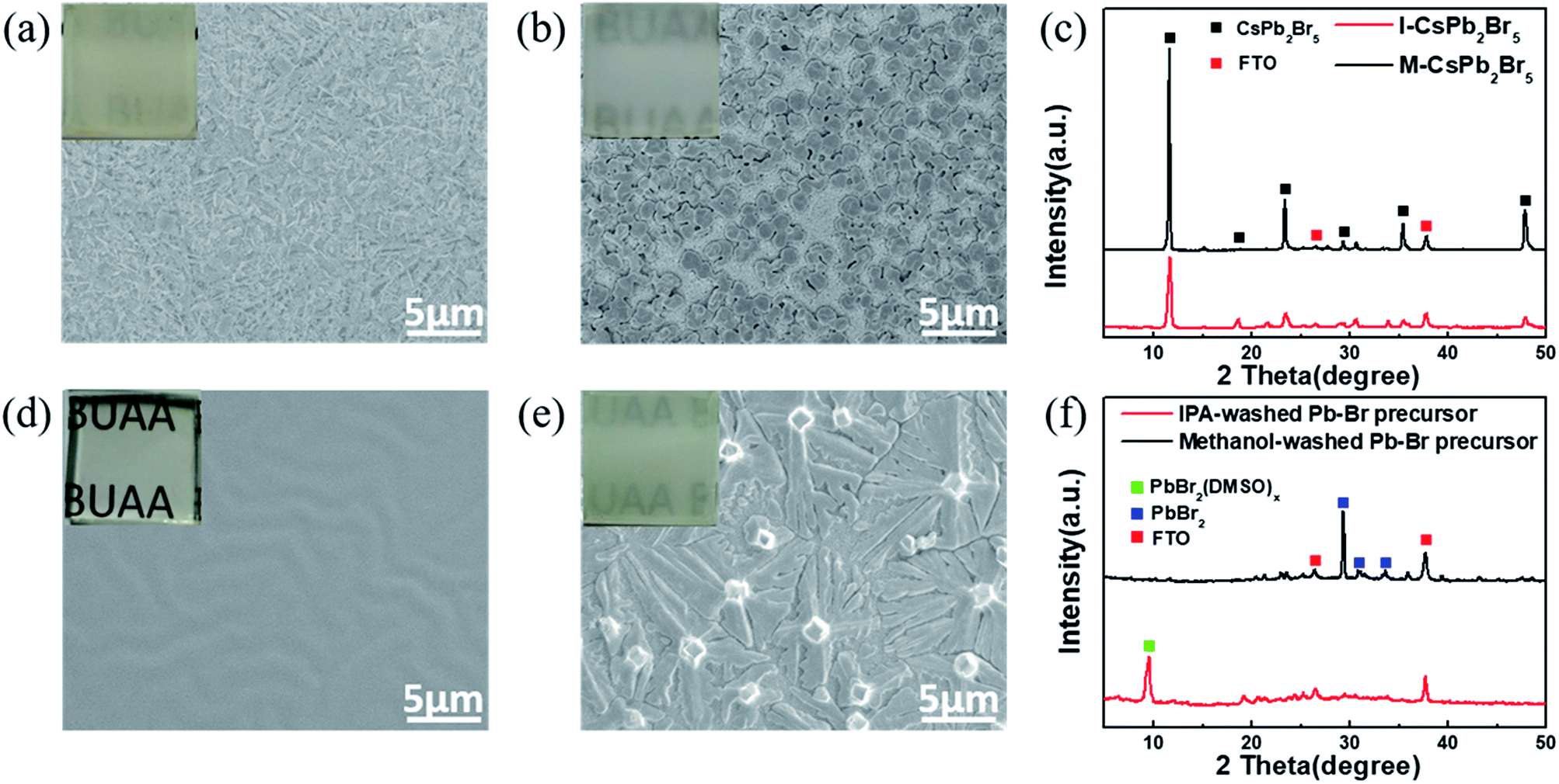 | ||
| Fig. 2 SEM images of (a) I-CsPb2Br5, (b) M-CsPb2Br5, (d) IPA-washed Pb–Br precursor, and (e) methanol-washed Pb–Br precursor. The insets are the corresponding optical photographs. (c) and (f) XRD patterns of the above corresponding films. | ||
On the basis of the above experimental phenomena, it is obvious that the solvent plays a dominant role in determining the microstructure of the CsPb2Br5 film. In order to highlight the solvent effect, the Pb–Br precursor films were immersed into bare solvents without PbBr2. As seen in Fig. 2d, the Pb–Br precursor film maintains a transparent appearance and smooth morphology after being immersed in IPA. The film keeps the substrate fully covered and the grain boundaries are almost unrecognizable. In comparison, immersion in methanol makes the film rapidly turn white in color and it is indicated in Fig. 2e that a rough surface with fibrous crystals is formed. The film has a dendritic crystal form with the crystals spreading on the substrate without sharing grain boundaries, which makes the mesoporous TiO2 layer visible. The XRD patterns in Fig. 2f indicate that the diffraction peak at 9.4° is still very intense for the IPA-washed Pb–Br precursor film, suggesting the presence of a PbBr2(DMSO)x adduct in the final film.31–33 For the methanol-washed Pb–Br precursor film, no diffraction peak corresponding to the PbBr2(DMSO)x adduct is detected, and the diffraction peaks at 29.1°, 30.5° and 33.9° can be indexed to the (201), (211) and (031) planes of PbBr2 (PDF#31-0679), respectively. Therefore, DMSO molecules seem to be washed away from the film. We proposed that the solvent polarity difference may be the cause for the different phenomena and a higher polarity might favor the release of DMF and DMSO molecules from the Pb–Br precursor film. Based on the above analysis, it could be concluded that the interaction between the solvent and the PbBr2(DMSO)x adduct is the main cause of the morphology and composition differences between the I-CsPb2Br5 and M-CsPb2Br5 films.
In order to convert the CsPb2Br5 intermediate into CsPbBr3 completely and rapidly, it is necessary to use appropriate reaction conditions. Since CsBr has a low solubility in IPA (∼1.7 mg ml−1), it would take a long time (e.g. tens of minutes) to obtain CsPbBr3 in the CsBr–IPA solution system. As a result, as shown in Fig. S1,† a large amount of CsPb2Br5 still remained in the film obtained by the above method. In addition, it is difficult to get a good morphology in such a CsBr solution. To accelerate the conversion, a high-concentration CsBr solution with methanol as the solvent was chosen.
To obtain CsPbBr3, the I- and M-CsPb2Br5 intermediates were immersed in a 17 mg ml−1 CsBr methanol solution at 50 °C for 5 min (the optimization of the conversion time was conducted and the results are shown in Fig. S2†), followed by annealing at 250 °C for 5 min (named as I-CsPbBr3 and M-CsPbBr3, respectively). Fig. 3a illustrates the phase transition from tetragonal CsPb2Br5 (for which the lattice parameters are a = b = 8.483 Å, c = 15.250 Å, α = β = γ = 90.000°) to cubic CsPbBr3 (for which the lattice parameters are a = b = 5.827 Å, c = 5.891 Å, α = β = 90.000°, γ = 89.650°). The crystal structure of tetragonal CsPb2Br5 shows a 3D framework of corner-connected PbBr6 octahedra and the Cs ions in the crystal are sandwiched between the two layers of Pb–Br-coordinated polyhedral.34,35 In contrast, cubic CsPbBr3 (space group Pm3m) is formed through the reinsertion of CsBr into CsPb2Br5, in which the PbBr6 octahedra extend in three dimensions via sharing vertices and the Cs ions localize in the octahedral voids.36
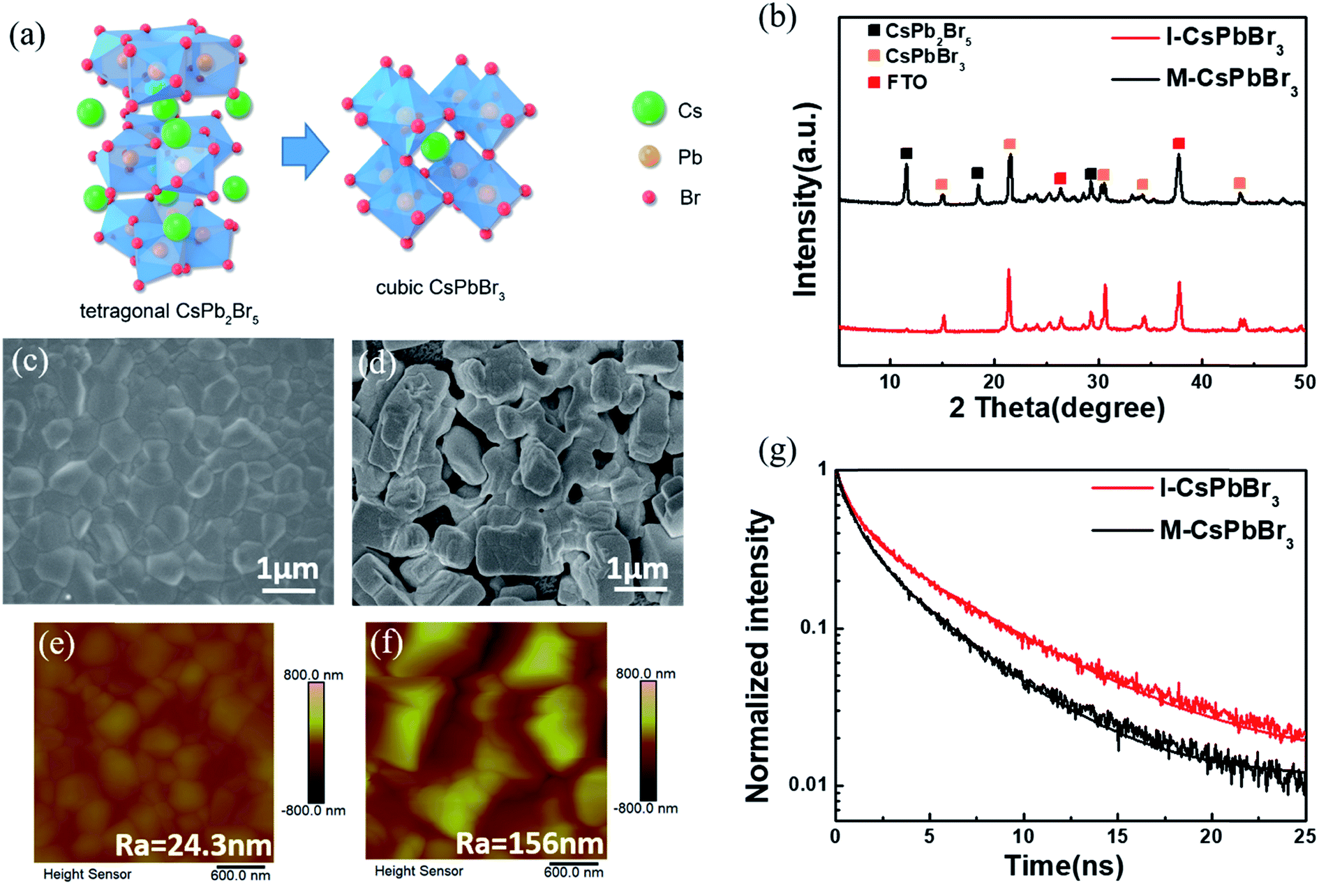 | ||
| Fig. 3 Characterization of the CsPbBr3 films. (a) Crystal structure of tetragonal CsPb2Br5 and cubic CsPbBr3. (b) XRD patterns, (c) and (d) SEM images, (e) and (f) AFM images, and (g) time-resolved PL spectra of the I-CsPbBr3 and M-CsPbBr3 films. | ||
Fig. 3b shows the XRD patterns of the I-CsPbBr3 and M-CsPbBr3 layers. The obvious diffraction peaks at 15.2°, 21.5°, 30.7°, 34.2° and 44.1° correspond to the (100), (110), (200), (210) and (220) planes of the cubic CsPbBr3 phase (PDF#18-0364), respectively. The conversion can be summarized as:
| CsPb2Br5 + CsBr → 2CsPbBr3 |
The major peaks of cubic CsPbBr3 for the I-CsPbBr3 film are slightly more intense than those for the M-CsPbBr3 film, demonstrating an improvement in crystallinity. Moreover, the obvious peaks at 11.7°, 18.8° and 29.4° for the M-CsPbBr3 film can be indexed to the characteristic planes of CsPb2Br5, indicating the incomplete conversion of CsPb2Br5. Obviously, the appropriate intermediate structure has a significant impact on the conversion degree.
Fig. 3c–f present the top-view SEM and AFM images of the I-CsPbBr3 and M-CsPbBr3 films. As indicated, the I-CsPbBr3 layer fully covers the TiO2 substrate (Fig. 3c). For the M-CsPbBr3 layer, a rather rough surface with larger loosely dispersed cubic crystals is observed (Fig. 3d). The compact surface and smaller grain size of the I-CsPbBr3 layer led to an ultra-even and uniform surface with a significantly smaller roughness (Ra) of 24.3 nm, as confirmed by the AFM image (Fig. 3e). Because the M-CsPb2Br5 film possess a large pore size and poor coverage, it leads to an inhomogeneous and discontinuous layer. Moreover, the reaction between the CsPb2Br5 intermediate and CsBr is a solid–liquid interfacial reaction. The I-CsPb2Br5 layer with a porous surface morphology and smaller crystal grains can effectively promote diffusion during the solid–liquid interfacial reaction with CsBr and restrict the chaotic and excessive growth of CsPbBr3 crystals. However, the CsPbBr3 crystals formed at the surface of the large and isolated bulk M-CsPb2Br5 crystals would suppress the interfacial reaction. Consequently, many large gaps between the crystals are generated and the grain size is abnormally large due to unrestricted phase transformation. As a result, the M-CsPbBr3 layer exhibits a fairly high Ra of 156 nm (Fig. 3f).
UV-vis spectroscopy, and steady-state and time-resolved PL were carried out to investigate the optical properties and charge transport dynamics of the CsPbBr3 films on glass substrates. As shown in Fig. S3 and S4,† the UV-vis absorption onsets of both films are at ∼540 nm, while the PL emission peaks of both films are at ∼535 nm, which is in line with the known absorption onset and bandgap of cubic CsPbBr3.19 Compared to the M-CsPbBr3 film, the I-CsPbBr3 film shows stronger PL intensity, indicating a higher crystallinity with less defect sites.37Fig. 3g presents the time-resolved PL (TRPL) curves that have been fitted by using a biexponential decay function.38 The PL decay lifetime (τave) for the M-CsPbBr3 film is calculated to be 3.26 ns, while the τave for the I-CsPbBr3 film is about 5.32 ns. The lower TRPL decay rate of I-CsPbBr3 indicates higher crystal quality, which is consistent with other characterization results as mentioned above.
Compared to the commonly used precursor (e.g. PbBr2), this porous CsPb2Br5 intermediate layer shows much promise to obtain pure and high-quality CsPbBr3 in a much shorter time. The results in Fig. S5† confirm the above statements. In addition, direct immersion of the Pb–Br precursor into a 17 mg ml−1 CsBr methanol solution would also produce CsPbBr3 films, but the morphology is poor and there is much residual CsPb2Br5 in the film (Fig. S6†), and the photovoltaic performance of the C-PSC is much lower than that based on the CsPbBr3 film fabricated from the porous CsPb2Br5 intermediate layer.
To evaluate the device photovoltaic performances, C-PSCs with the structure of FTO/c-TiO2/m-TiO2/CsPbBr3/carbon were fabricated, as illustrated in Fig. 4a. Fig. 4b presents a cross-sectional SEM image of the I-CsPbBr3 C-PSC, showing a 400 nm-thick m-TiO2/CsPbBr3 layer and a 350 nm-thick upper CsPbBr3 layer. Because of the dense and uniform surface of the I-CsPbBr3 layer, there is almost no interspace between the carbon electrode and the perovskite. The energy level diagram of the device and the transfer path of photogenerated carriers are shown in Fig. 4c, indicating the smooth electron injection from the CsPbBr3 conduction band (CB) to the TiO2 CB and hole injection from the CsPbBr3 valence band (VB) to the carbon electrode.
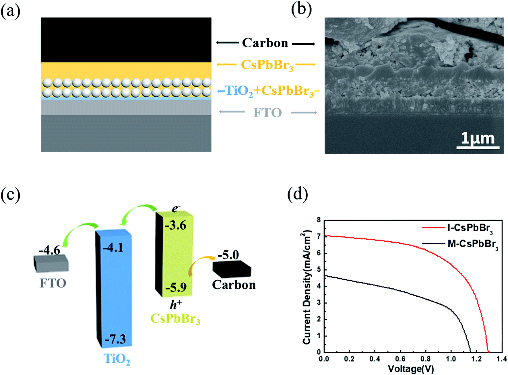 | ||
| Fig. 4 Structure and photovoltaic performance of CsPbBr3 C-PSCs. (a) Schematic diagram and (b) cross-sectional SEM images of the CsPbBr3 C-PSCs. (c) Working principle and (d) J–V curves of the C-PSCs based on I-CsPbBr3 and M-CsPbBr3 films. | ||
The current density–voltage (J–V) curves and the corresponding photovoltaic parameters of the I-CsPbBr3 and M-CsPbBr3 C-PSCs are presented in Fig. 4d and Table 1, respectively. The I-CsPbBr3 device obtained a PCE of 5.38% with a Voc of 1.29 V, a Jsc of 7.07 mA cm−2 and a FF of 0.58. In comparison, the M-CsPbBr3 device displays an inferior performance with a PCE of 2.68%, a Voc of 1.15 V, a Jsc of 4.66 mA cm−2 and a FF of 0.50. Obviously, I-CsPbBr3 films with a higher perovskite coverage and smoother surfaces are desired for highly efficient C-PSCs, especially for the enhancement of the Voc and FF.39 In comparison, the pores and fractures on the M-CsPbBr3 film would result in direct contact between TiO2 and the carbon electrode, significantly increasing the charge recombination loss. Moreover, M-CsPbBr3 has coarse grains and obvious morphology fluctuation, which would weaken the interfacial contact with the carbon electrode. In addition to the structure, the incomplete conversion of CsPb2Br5 in the M-CsPbBr3 films would prohibit charge transport and limit the device performance. In addition, I-CsPbBr3 shows longer carrier lifetime, indicating less possibility for nonradiative recombination in C-PSCs.16
| Devices | V oc (V) | J sc (mA cm−2) | FF (%) | PCE (%) |
|---|---|---|---|---|
| I-CsPbBr3 | 1.29 | 7.07 | 59 | 5.38 |
| M-CsPbBr3 | 1.15 | 4.66 | 50 | 2.68 |
In order to further optimize the photovoltaic performances of the PSCs, the formation mechanism of the critical IPA–CsPb2Br5 intermediates requires more in-depth analysis and discussion. Fig. 5a shows the XRD patterns of the original Pb–Br precursor film and the IPA–CsPb2Br5 intermediates with different immersion durations in 1.7 mg ml−1 CsBr–IPA solution (30, 60, 120, 240 and 480 s). The Pb–Br precursor film shows an obvious diffraction peak at 9.4°, which is the fingerprint of the PbBr2(DMSO)x adduct. As the immersion time increases, the diffraction peaks at 11.7°, 18.8°, 23.4°, 29.4°, 35.5°and 47.9°, corresponding to the tetragonal CsPb2Br5 phase, appear and gradually become stronger. When the immersion time is increased to over 240 s, the diffraction peak of the PbBr2(DMSO)x adduct almost disappears. As discussed above, it can be concluded that the formation process of the CsPb2Br5 intermediate can be written as:
| 2PbBr2(DMSO)x + CsBr → CsPb2Br5 + 2xDMSO |
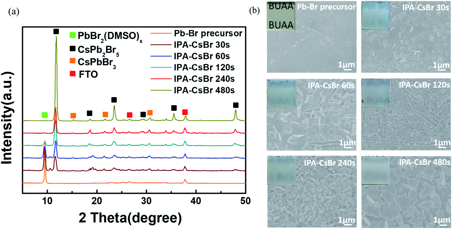 | ||
| Fig. 5 Effects of reaction time in low-concentration CsBr solution on the structure and morphology of the CsPb2Br5 intermediates. (a) XRD patterns and (b) SEM images of the CsPb2Br5 intermediate films with different reaction times (30, 60, 120, 240 and 480 s). The insets in (b) are the corresponding optical photographs. | ||
Additionally, the weak diffraction peaks at 15.2°, 21.5° and 30.7° that could be indexed to the characteristic peaks of the cubic CsPbBr3 phase are also detected for the sample under long immersion times, meaning the generation of a small amount of CsPbBr3.
Top-view SEM images and optical photographs were further taken for the IPA–CsPb2Br5 intermediates at different immersion times, which are displayed in Fig. 5b. Except for the original Pb–Br precursor film, the other IPA–CsPb2Br5 intermediate films exhibit a white color, which gradually became darker as the immersion time increased. As seen in the SEM images, the original Pb–Br precursor film is flat and compact. However, significant differences could be easily found for the CsPb2Br5 intermediate films after reaction. When the immersion time is 30 s, the previously fully covered Pb–Br precursor film is cracked and the integrity is destroyed, with some fibrous crystals appearing. On increasing the reaction time to 60 s, the film becomes more fragmented and more fibrous crystals are formed. As the immersion time further increases to 120 s, fibrous crystals completely cover the substrate. It is particularly noteworthy that when the conversion time reaches 240 s, the fibrous crystal structure undergoes an abnormal change with a decrease in the grain size, and as a result the film seems to consist of porous lamellar branched crystals. On further extending the reaction time to 480 s, obviously larger crystals appear and the flat crystals overlap with each other to cover the substrate. The increase in crystal size may be due to the Ostwald ripening effect under long reaction times.40
Fig. 6a and b present the XRD patterns and top-view SEM images (including optical photographs) of the CsPbBr3 films obtained from the above-mentioned different I-CsPb2Br5 intermediate layers. Here, samples 1#, 2#, 3#, 4# and 5# refer to the CsPbBr3 films converted from the I-CsPb2Br5 intermediate layers at the reaction time of 30 s, 60 s, 120 s, 240 s and 480 s in the IPA–CsBr solution, respectively. The transformed perovskite thin films exhibit the cubic CsPbBr3 crystal structure with strong diffraction peaks at 15.2°, 21.5°, 30.7°, 34.2° and 44.1°. Although the formation of the cubic CsPbBr3 phase is confirmed by XRD, the characteristic peaks at 11.7° and 29.4° of CsPb2Br5 could be obviously observed due to the incomplete conversion of the intermediates to perovskites. Apparently, the fraction of the cubic CsPbBr3 phase increases until the reaction time in the low-concentration CsBr solution reaches 240 s. The completeness of the conversion for sample 5# is far less than that of sample 4#. As indicated in Fig. 6b, sample 1# shows a poor film quality with many distinct grain protrusions and lots of pinholes on the surface. From sample 1# to sample 4#, the surface roughness is continuously reduced, and the film integrity is continuously improved. In addition, the grains tend to be more tightly packed and the grain size distribution becomes narrow. For sample 5#, the surface coverage is markedly deteriorated, and the film becomes rougher. Crystal grains with irregular shapes and sizes appear. As indicated above (Fig. 2), the large polarity methanol solvent would quickly destroy the structure of the PbBr2(DMSO)x adduct. Therefore, for the CsPb2Br5 intermediate films containing a large fraction of PbBr2(DMSO)x adduct, such as IPA–Pb–Br at 30 s, 60 s and 120 s, the further conversion in 17 mg ml−1 CsBr methanol solution would more or less destroy the film structure, leading to rough samples 1#, 2#, and 3# with poor coverage. From sample 1# to 4#, the gradual decrease in PbBr2(DMSO)x adduct in the intermediates improves the morphology and enhances the purity of the CsPbBr3 films. In addition, the gradual decrease in the crystal size and the increase in the porosity of the CsPb2Br5 intermediate would also promote the penetration of the CsBr solution to implement conversion. As a result, sample 4# exhibits the best morphology and the least residual CsPb2Br5 intermediate. The roughness and residual CsPb2Br5 are increased for sample 5#, which may be related to the increase in the crystal size in IPA-480 s CsPb2Br5. The randomly aligned large CsPb2Br5 crystals would not only increase the roughness of the CsPbBr3 films (sample 5#) but also slow the conversion in the interior of the CsPb2Br5 crystals due to the difficulty in the penetration of the CsBr solution.
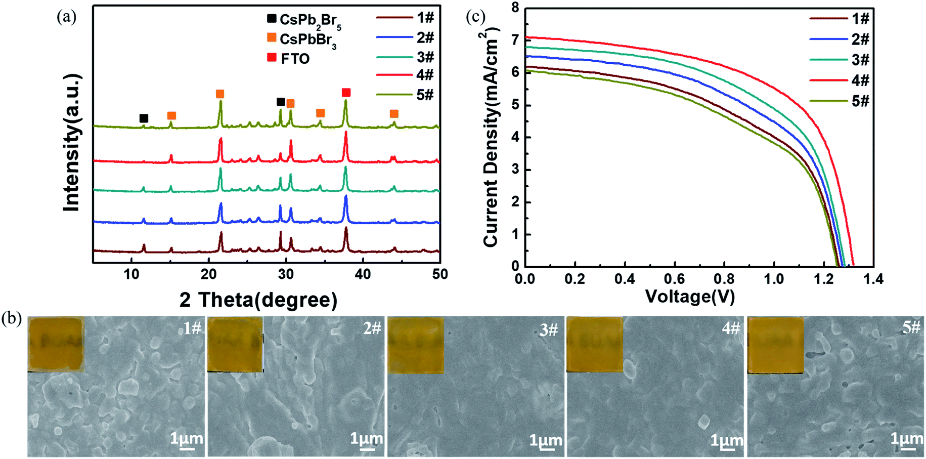 | ||
| Fig. 6 Effects of reaction time in low-concentration CsBr solution on the structure, morphology and photovoltaic performance of the CsPbBr3 films. (a) XRD patterns and (b) SEM images of the 1#–5# CsPbBr3 films (1#–5# corresponding to the reaction time of 30, 60, 120, 240 and 480 s, respectively). The insets in (b) are the corresponding optical photographs. (c) J–V curves of the C-PSCs based on the 1#–5# CsPbBr3 films. | ||
To further evaluate the photovoltaic performance, the above CsPbBr3 layers were used to fabricate C-PSCs. The J–V curves of the different devices are illustrated in Fig. 6c and the calculated photovoltaic parameters are listed in Table 2. Device 1# exhibits a relatively low performance with a Voc of 1.26 V, Jsc of 6.20 mA cm−2, FF of 0.52 and PCE of 4.06%. Meanwhile, for device 2# and device 3#, the photovoltaic performance continues to increase, which is mainly caused by the improvement of the surface quality and perovskite purity of the CsPbBr3 film as mentioned in Fig. 6a and b. Evidently, impressively higher performance is obtained by device 4# with a Voc of 1.32 V, Jsc of 7.10 mA cm−2, FF of 0.60 and PCE of 5.62% due to the enhanced perovskite crystallinity and quality, which reduced the grain boundaries and led to better interface contact. The photovoltaic performance is obviously decreased for device 5# with a Voc of 1.25 V, Jsc of 6.07 mA cm−2, FF of 0.51 and PCE of 3.87%. The poor performance of device 5# is easily interpreted as the excessive residual CsPb2Br5 would suppress charge transport, and the rough surface of the CsPbBr3 film would result in bad interface contact.41,42
| Devices | V oc (V) | J sc (mA cm−2) | FF (%) | PCE (%) |
|---|---|---|---|---|
| 1# | 1.26 | 6.20 | 52 | 4.06 |
| 2# | 1.27 | 6.50 | 54 | 4.46 |
| 3# | 1.28 | 6.80 | 56 | 4.87 |
| 4# | 1.32 | 7.10 | 60 | 5.62 |
| 5# | 1.25 | 6.07 | 51 | 3.87 |
After preliminary optimization, the champion CsPbBr3 C-PSC fabricated from sample 4# yields a PCE of 6.10% with a Voc of 1.38 V, a Jsc of 7.13 mA cm−2 and a FF of 0.62 (Fig. 7a). A performance comparison between the previously reported CsPbBr3 PSCs and our present device is provided in Table S1.†14,18,19,21–26,43,44 Considering the bandgap of CsPbBr3 (∼2.3 eV), a 0.92 V voltage loss exists for the Voc of the champion device. In addition, the obtained Jsc is also much lower than the maximum theoretical photocurrent density (about 9 mA cm−2). The large energy differences at the TiO2 (ECB = −4.0 eV)/CsPbBr3 (ECB = −3.3 eV) interface and CsPbBr3 (EVB = −5.6 eV)/carbon electrode (work function ∼ 5.0 eV) may slow carrier extraction and limit the photovoltaic performance of the C-PSCs. To ensure the reliability of the J–V measurement, the steady current density as a function of time for the champion device was collected (Fig. 7b). The stabilized PCE output is calculated to be about 5.80% for over 300 s. J–V curves with different scanning directions were further recorded to examine the hysteresis effects.45 The champion device shows a small hysteresis with a hysteresis index below 7% (Fig. S7†). As revealed in Fig. 7c, the IPCE values of the champion device are over 75% in the wavelength range from 380 to 500 nm and the onset is at around 530 nm, which is consistent with the steady-state PL of CsPbBr3 (Fig. 3g). The photocurrent density integrated from the IPCE spectrum is 6.41 mA cm−2, which is close to the Jsc extracted from the J–V curve. For reproducibility evaluation, 30 individual devices with the same fabrication procedure to that of the champion device were fabricated and characterized. The PCE histogram of these devices shows a narrow distribution with an average value of 5.32%. To prove the universal character of this method for different substrates, C-PSCs with a planar structure of FTO/bl-TiO2/CsPbBr3/carbon were also fabricated, which yield a PCE of about 4% (Fig. S8†).
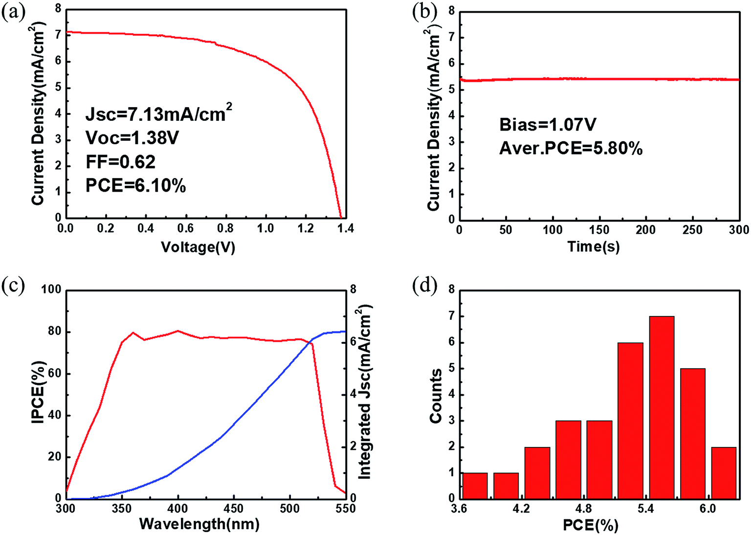 | ||
| Fig. 7 Performance of the champion C-PSC. (a) J–V curve, (b) steady current density at a voltage close to the maximum output point, and (c) IPCE spectrum of the champion CsPbBr3 C-PSC. (d) PCE histogram of 30 separate devices. | ||
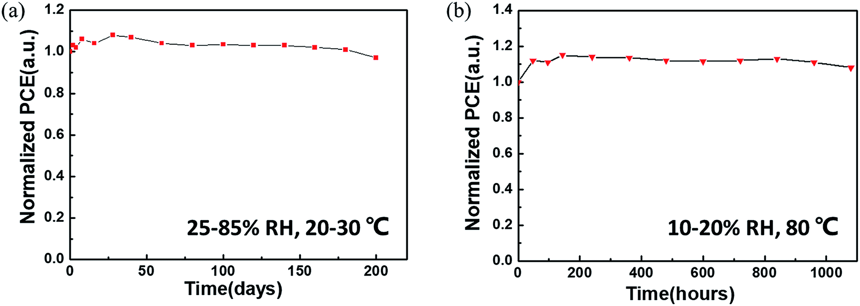
The ambient stability and thermal stability of the non-encapsulated CsPbBr3 C-PSCs were further evaluated. As is well-known, CsPbBr3 has remarkable ambient stability even at relatively high temperature.18 The introduction of a carbon electrode is more conducive to the long-term stability of the device. In an air atmosphere (25–85% relative humidity (RH) and a temperature of 20–30 °C), the PCE of the CsPbBr3 C-PSC remains at 97% of its initial value after 200 days of storage (Fig. 8a). Furthermore, the PCE of the CsPbBr3 C-PSC exhibits almost no degradation (even being slightly higher than its initial value) in an ambient environment with persistent thermal attack at 80 °C and 10–20% RH for more than 1080 h (Fig. 8b).
 | ||
| Fig. 8 Device stability. (a) Normalized PCEs of CsPbBr3 C-PSCs as a function of storage time in the ambient environment (25–85% RH, 20–30 °C) without encapsulation. (b) Normalized PCEs of CsPbBr3 C-PSCs as a function of time at 80 °C in the ambient environment (10–20% RH) without encapsulation. | ||
Conclusions
We have demonstrated the successful deposition of a high-quality CsPbBr3 layer by employing a porous CsPb2Br5 intermediate layer. The porous CsPb2Br5 intermediate layer with full film coverage was prepared by lowering the CsBr concentration to widen the processing window of CsPb2Br5 and choosing a lower polarity solvent (IPA). A flat and high coverage CsPbBr3 layer was obtained by converting the porous CsPb2Br5 layer in a high-concentration CsBr solution. The C-PSCs based on the optimized CsPbBr3 layer achieved a PCE of 6.1%. The CsPbBr3 C-PSCs without encapsulation show almost no PCE decay after 200 days of storage in ambient air (25–85% RH, 20–30 °C) and at 80 °C (10–20% RH) for over 1080 h. Therefore, the porous CsPb2Br5 layer shows much promise for preparing high-quality CsPbBr3 layers for efficient and stable PSCs.Experimental
Fabrication of CsPbBr3 PSCs
FTO glass (TEC15, NSG) was washed with soap water, DI-water, ethanol, and isopropanol sequentially. Then, a TiO2 blocking layer (0.15 M titanium diisopropoxide bis-(acetylacetonate) in 1-butanol solution) was deposited on the FTO glass (17 mm × 17 mm) at 2000 rpm for 20 s and heated at 125 °C for 5 min. The mesoporous TiO2 layer was deposited on the TiO2 blocking layer (bl-TiO2) at 5000 rpm for 30 s and sintered at 550 °C for 120 min using a commercial TiO2 paste (Dyesol 30 NRD, Dyesol) diluted by ethanol with a weight ratio of 1![[thin space (1/6-em)]](https://www.rsc.org/images/entities/char_2009.gif) :2.5.46
:2.5.46
The perovskite film was fabricated by a modified two step method.47,48 The Pb–Br precursor films were spin-coated onto mesoporous TiO2 layers at 2000 rpm for 20 s using 1.4 M PbBr2 solution in a mixed solvent of dimethylformamide (DMF) and dimethyl sulfoxide (DMSO) (9:1 volume ratio). The Pb–Br precursor films were then immediately dipped into 1.7 mg ml−1 CsBr–isopropanol (IPA) solution (CsBr–IPA saturated solution) for different reaction times or into 1.7 mg ml−1 CsBr–methanol solution for 240 s at room temperature. Then, the resulting intermediate films were immersed into 17 mg ml−1 CsBr methanol solution for 5 min at 50 °C. The obtained films were washed with IPA, followed by heating at 250 °C for 5 min to get CsPbBr3 films.19
Finally, commercial carbon paste (MTW-CE-C-003, Shanghai MaterWin New Materials Co., Ltd.) was painted on the CsPbBr3 layers, followed by heating at 110 °C for 30 min.14,49 All the fabrication steps above were conducted in ambient air.
Characterization
Surface and cross-section morphologies were observed using a JSM-7500F field emission scanning electron microscope (FESEM). X-ray diffraction (XRD) patterns were collected with a Rigaku D/MAX-2500 X-ray diffractometer using Cu Kα radiation (λ = 0.1541 nm) with a speed of 6° min−1. Absorption spectra were measured on a UV-3000 ultraviolet and visible (UV-vis) spectrophotometer. The photoluminescence (PL) spectra were obtained on a lifetime and steady state spectrometer (FLS920, Edinburgh Instruments Ltd.) with an excitation wavelength of 515 nm at room temperature. Surface roughnesses were characterized using a Bruker Dimension ICON atomic force microscope (AFM). The optical photographs were taken using a digital camera (Olympus E-PL1, Japan) with BUAA printed on a white background.The J–V measurements were recorded on a Zahner photo-electrochemical workstation with the scans (a voltage step of 50 mV and a delay time of 100 ms) performed under the illumination of a solar simulator (Newport SOL3A 94023A, 100 mW cm−2, AM 1.5), and the intensity was calibrated with a certified Si-reference cell (Newport). IPCE spectra were recorded on an IPCE kit (E0201, Institute of Physics, Chinese Academy of Sciences). For the stability test at room temperature (20–30 °C), the devices were stored in ambient air (RH ∼ 25–85%). For the heat stress tests, the devices were stored in an oven (80 °C) in dry air (RH ∼ 10–20%). J–V curves were measured periodically to obtain the photovoltaic parameters. All of the above characterizations were carried out in ambient air.
Conflicts of interest
There are no conflicts to declare.Acknowledgements
This work was financially supported by the Young Talent of “Zhuoyue” Program of Beihang University, the National Natural Science Foundation of China (No. 21603010) and the Beijing Natural Science Foundation (No. 2182031).References
- A. Kojima, K. Teshima, Y. Shirai and T. Miyasaka, Organometal Halide Perovskites as Visible-Light Sensitizers for Photovoltaic Cells, J. Am. Chem. Soc., 2009, 131, 6050–6051 CrossRef CAS PubMed.
- A. Mei, X. Li, L. Liu, Z. Ku, T. Liu, Y. Rong, M. Xu, M. Hu, J. Chen, Y. Yang, M. Grätzel and H. Han, A hole-conductor-free, fully printable mesoscopic perovskite solar cell with high stability, Science, 2014, 345, 295–298 CrossRef CAS PubMed.
- H. Zhou, Q. Chen, G. Li, S. Luo, T.-B. Song, H.-S. Duan, Z. Hong, J. You, Y. Liu and Y. Yang, Interface engineering of highly efficient perovskite solar cells, Science, 2014, 345, 542–546 CrossRef CAS PubMed.
- W. S. Yang, J. H. Noh, N. J. Jeon, Y. C. Kim, S. Ryu, J. Seo and S. I. Seok, High-performance photovoltaic perovskite layers fabricated through intramolecular exchange, Science, 2015, 348, 1234–1237 CrossRef CAS PubMed.
- X. Li, D. Bi, C. Yi, J.-D. Décoppet, J. Luo, S. M. Zakeeruddin, A. Hagfeldt and M. Grätzel, A vacuum flash-assisted solution process for high-efficiency large-area perovskite solar cells, Science, 2016, 353, 58–62 CrossRef CAS PubMed.
- W. S. Yang, B.-W. Park, E. H. Jung, N. J. Jeon, Y. C. Kim, D. U. Lee, S. S. Shin, J. Seo, E. K. Kim, J. H. Noh and S. I. Seok, Iodide management in formamidinium-lead-halide-based perovskite layers for efficient solar cells, Science, 2017, 356, 1376–1379 CrossRef CAS PubMed.
- N. J. Jeon, H. Na, E. H. Jung, T.-Y. Yang, Y. G. Lee, G. Kim, H.-W. Shin, S. Il Seok, J. Lee and J. Seo, A fluorene-terminated hole-transporting material for highly efficient and stable perovskite solar cells, Nat. Energy, 2018, 3, 682–689 CrossRef CAS.
- Chart of Best Research-Cell Efficiencies Provided by NREL. (accessed: July 2018). https://www.nrel.gov/pv/assets/images/efficiency-chart-20180716.jpg.
- D. Wang, M. Wright, N. K. Elumalai and A. Uddin, Stability of perovskite solar cells, Sol. Energy Mater. Sol. Cells, 2016, 147, 255–275 CrossRef CAS.
- N.-G. Park, M. Grätzel, T. Miyasaka, K. Zhu and K. Emery, Towards stable and commercially available perovskite solar cells, Nat. Energy, 2016, 1, 16152 CrossRef CAS.
- H.-S. Kim, J.-Y. Seo and N.-G. Park, Material and Device Stability in Perovskite Solar Cells, ChemSusChem, 2016, 9, 2528–2540 CrossRef CAS PubMed.
- R. E. Beal, D. J. Slotcavage, T. Leijtens, A. R. Bowring, R. A. Belisle, W. H. Nguyen, G. F. Burkhard, E. T. Hoke and M. D. McGehee, Cesium Lead Halide Perovskites with Improved Stability for Tandem Solar Cells, J. Phys. Chem. Lett., 2016, 7, 746–751 CrossRef CAS PubMed.
- J. K. Nam, S. U. Chai, W. Cha, Y. J. Choi, W. Kim, M. S. Jung, J. Kwon, D. Kim and J. H. Park, Potassium Incorporation for Enhanced Performance and Stability of Fully Inorganic Cesium Lead Halide Perovskite Solar Cells, Nano Lett., 2017, 17, 2028–2033 CrossRef CAS PubMed.
- X. Chang, W. Li, L. Zhu, H. Liu, H. Geng, S. Xiang, J. Liu and H. Chen, Carbon-Based CsPbBr3 Perovskite Solar Cells: All-Ambient Processes and High Thermal Stability, ACS Appl. Mater. Interfaces, 2016, 8, 33649–33655 CrossRef CAS PubMed.
- S. Xiang, W. Li, Y. Wei, J. Liu, H. Liu, L. Zhu and H. Chen, The synergistic effect of non-stoichiometry and Sb-doping on air-stable α-CsPbI3 for efficient carbon-based perovskite solar cells, Nanoscale, 2018, 10, 9996–10004 RSC.
- S. Xiang, Z. Fu, W. Li, Y. Wei, J. Liu, H. Liu, L. Zhu, R. Zhang and H. Chen, Highly Air-Stable Carbon-Based α-CsPbI3 Perovskite Solar Cells with a Broadened Optical Spectrum, ACS Energy Lett., 2018, 1824–1831 CrossRef CAS.
- J. Liang, Z. Liu, L. Qiu, Z. Hawash, L. Meng, Z. Wu, Y. Jiang, L. K. Ono and Y. Qi, Enhancing Optical, Electronic, Crystalline, and Morphological Properties of Cesium Lead Halide by Mn Substitution for High-Stability All-Inorganic Perovskite Solar Cells with Carbon Electrodes, Adv. Energy Mater., 2018, 1800504 CrossRef.
- M. Kulbak, S. Gupta, N. Kedem, I. Levine, T. Bendikov, G. Hodes and D. Cahen, Cesium Enhances Long-Term Stability of Lead Bromide Perovskite-Based Solar Cells, J. Phys. Chem. Lett., 2016, 7, 167–172 CrossRef CAS PubMed.
- J. Liang, C. Wang, Y. Wang, Z. Xu, Z. Lu, Y. Ma, H. Zhu, Y. Hu, C. Xiao, X. Yi, G. Zhu, H. Lv, L. Ma, T. Chen, Z. Tie, Z. Jin and J. Liu, All-Inorganic Perovskite Solar Cells, J. Am. Chem. Soc., 2016, 138, 15829–15832 CrossRef CAS PubMed.
- H. Chen, S. Xiang, W. Li, H. Liu, L. Zhu and S. Yang, Inorganic Perovskite Solar Cells: A Rapidly Growing Field, Sol. RRL, 2018, 2, 1700188 CrossRef.
- M. Kulbak, D. Cahen and G. Hodes, How Important Is the Organic Part of Lead Halide Perovskite Photovoltaic Cells? Efficient CsPbBr3 Cells, J. Phys. Chem. Lett., 2015, 6, 2452–2456 CrossRef CAS PubMed.
- X. Ding, Y. Ren, Y. Wu, Y. Xu, J. Zhu, T. Hayat, A. Alsaedi, Z. Li, Y. Huang and S. Dai, Sequential deposition method fabricating carbon based fully-inorganic perovskite solar cells, Sci. China Mater., 2018, 61, 73–79 CrossRef.
- J. Duan, Y. Zhao, B. He and Q. Tang, High-Purity Inorganic Perovskite Films for Solar Cells with 9.72% Efficiency, Angew. Chem., Int. Ed., 2018, 130, 3849–3853 CrossRef.
- P. Teng, X. Han, J. Li, Y. Xu, L. Kang, Y. Wang, Y. Yang and T. Yu, Elegant Face-Down Liquid-Space-Restricted Deposition of CsPbBr3 Films for Efficient Carbon-Based All-Inorganic Planar Perovskite Solar Cells, ACS Appl. Mater. Interfaces, 2018, 10, 9541–9546 CrossRef CAS PubMed.
- K. C. Tang, P. You and F. Yan, Highly Stable All-Inorganic Perovskite Solar Cells Processed at Low Temperature, Sol. RRL, 2018, 1800075 CrossRef.
- J. Duan, Y. Zhao, B. He and Q. Tang, Simplified Perovskite Solar Cell with 4.1% Efficiency Employing Inorganic CsPbBr3 as Light Absorber, Small, 2018, 14, 1704443 CrossRef PubMed.
- W. Li, J. Fan, J. Li, Y. Mai and L. Wang, Controllable Grain Morphology of Perovskite Absorber Film by Molecular Self-Assembly toward Efficient Solar Cell Exceeding 17%, J. Am. Chem. Soc., 2015, 137, 10399–10405 CrossRef CAS PubMed.
- N. Ahn, D.-Y. Son, I.-H. Jang, S. M. Kang, M. Choi and N.-G. Park, Highly Reproducible Perovskite Solar Cells with Average Efficiency of 18.3% and Best Efficiency of 19.7% Fabricated via Lewis Base Adduct of Lead(II) Iodide, J. Am. Chem. Soc., 2015, 137, 8696–8699 CrossRef CAS PubMed.
- N. J. Jeon, J. H. Noh, Y. C. Kim, W. S. Yang, S. Ryu and S. I. Seok, Solvent engineering for high-performance inorganic-organic hybrid perovskite solar cells, Nat. Mater., 2014, 13, 897–903 CrossRef CAS PubMed.
- M. Yang, Z. Li, M. O. Reese, O. G. Reid, D. H. Kim, S. Siol, T. R. Klein, Y. Yan, J. J. Berry, M. F. A. M. van Hest and K. Zhu, Perovskite ink with wide processing window for scalable high-efficiency solar cells, Nat. Energy, 2017, 2, 17038 CrossRef CAS.
- A. D. Baranyi, M. Onyszchuk, Y. L. Page and G. Donnay, The crystal and molecular structure of lead (II) bromide-bis-dimethylsulphoxide, PbBr2·2[(CH3)2SO], Can. J. Chem., 1977, 55, 849–855 CrossRef CAS.
- H. Zhang, X. Liu, J. Dong, H. Yu, C. Zhou, B. Zhang, Y. Xu and W. Jie, Centimeter-Sized Inorganic Lead Halide Perovskite CsPbBr3 Crystals Grown by an Improved Solution Method, Cryst. Growth Des., 2017, 17, 6426–6431 CrossRef CAS.
- Y. Zhang, Y. Liang, Y. Wang, F. Guo, L. Sun and D. Xu, Planar FAPbBr3 Solar Cells with Power Conversion Efficiency above 10%, ACS Energy Lett., 2018, 1808–1814 CrossRef.
- K.-H. Wang, L. Wu, L. Li, H.-B. Yao, H.-S. Qian and S.-H. Yu, Large-Scale Synthesis of Highly Luminescent Perovskite-Related CsPb2Br5 Nanoplatelets and Their Fast Anion Exchange, Angew. Chem., Int. Ed., 2016, 55, 8328–8332 CrossRef CAS PubMed.
- G. Li, H. Wang, Z. Zhu, Y. Chang, T. Zhang, Z. Song and Y. Jiang, Shape and phase evolution from CsPbBr3 perovskite nanocubes to tetragonal CsPb2Br5 nanosheets with an indirect bandgap, Chem. Commun., 2016, 52, 11296–11299 RSC.
- G. Tong, H. Li, D. Li, Z. Zhu, E. Xu, G. Li, L. Yu, J. Xu and Y. Jiang, Dual-Phase CsPbBr3-CsPb2Br5 Perovskite Thin Films via Vapor Deposition for High-Performance Rigid and Flexible Photodetectors, Small, 2017, 14, 1702523 CrossRef PubMed.
- W. Zhu, C. Bao, B. Lv, F. Li, Y. Yi, Y. Wang, J. Yang, X. Wang, T. Yu and Z. Zou, Dramatically promoted crystallization control of organolead triiodide perovskite film by a homogeneous cap for high efficiency planar-heterojunction solar cells, J. Mater. Chem. A, 2016, 4, 12535–12542 RSC.
- Y. Bai, S. Xiao, C. Hu, T. Zhang, X. Meng, Q. Li, Y. Yang, K. S. Wong, H. Chen and S. Yang, A Pure and Stable Intermediate Phase is Key to Growing Aligned and Vertically Monolithic Perovskite Crystals for Efficient PIN Planar Perovskite Solar Cells with High Processibility and Stability, Nano Energy, 2017, 34, 58–68 CrossRef CAS.
- X. Chang, W. Li, H. Chen, L. Zhu, H. Liu, H. Geng, S. Xiang, J. Liu, X. Zheng, Y. Yang and S. Yang, Colloidal Precursor-Induced Growth of Ultra-Even CH3NH3PbI3 for High-Performance Paintable Carbon-Based Perovskite Solar Cells, ACS Appl. Mater. Interfaces, 2016, 8, 30184–30192 CrossRef CAS PubMed.
- H. Chen, Z. Wei, H. He, X. Zheng, K. S. Wong and S. Yang, Solvent Engineering Boosts the Efficiency of Paintable Carbon-Based Perovskite Solar Cells to Beyond 14%, Adv. Energy Mater., 2016, 6, 1502087 CrossRef.
- X. Zhang, Z. Li, Y. Ding, L. Hu, J. Ye, X. Pan and S. Dai, Highly efficient and stable perovskite solar cell prepared from an in situ pre-wetted PbI2 nano-sheet array film, Sustainable Energy Fuels, 2017, 1, 1056–1064 RSC.
- H. Chen, Two-Step Sequential Deposition of Organometal Halide Perovskite for Photovoltaic Application, Adv. Funct. Mater., 2017, 27, 1605654 CrossRef.
- P. Wang, X. Zhang, Y. Zhou, Q. Jiang, Q. Ye, Z. Chu, X. Li, X. Yang, Z. Yin and J. You, Solvent-controlled growth of inorganic perovskite films in dry environment for efficient and stable solar cells, Nat. Commun., 2018, 9, 2225 CrossRef PubMed.
- Z. Liu, B. Sun, X. Liu, J. Han, H. Ye, T. Shi, Z. Tang and G. Liao, Efficient Carbon-based CsPbBr3 Inorganic Perovskite Solar Cells by Using Cu-Phthalocyanine as Hole Transport Material, Nano-Micro Lett., 2018, 10, 34 CrossRef.
- Z. Wei, H. Chen, K. Yan, X. Zheng and S. Yang, Hysteresis-free multi-walled carbon nanotube-based perovskite solar cells with a high fill factor, J. Mater. Chem. A, 2015, 3, 24226–24231 RSC.
- J. H. Im, I. H. Jang, N. Pellet, M. Gratzel and N. G. Park, Growth of CH3NH3PbI3 cuboids with controlled size for high-efficiency perovskite solar cells, Nat. Nanotechnol., 2014, 9, 927–932 CrossRef CAS PubMed.
- T. Zhang, M. Yang, Y. Zhao and K. Zhu, Controllable Sequential Deposition of Planar CH3NH3PbI3 Perovskite Films via Adjustable Volume Expansion, Nano Lett., 2015, 15, 3959–3963 CrossRef CAS PubMed.
- G. Li, T. Zhang and Y. Zhao, Hydrochloric acid accelerated formation of planar CH3NH3PbI3 perovskite with high humidity tolerance, J. Mater. Chem. A, 2015, 3, 19674–19678 RSC.
- H. Chen and S. Yang, Carbon-Based Perovskite Solar Cells without Hole Transport Materials: The Front Runner to the Market?, Adv. Mater., 2017, 29, 1603994 CrossRef PubMed.
Footnote |
| † Electronic supplementary information (ESI) available. See DOI: 10.1039/c8se00442k |
| This journal is © The Royal Society of Chemistry 2019 |