
 Open Access Article
 This Open Access Article is licensed under a Creative Commons Attribution-Non Commercial 3.0 Unported Licence
Electrochemical synthesis of Au@semiconductor core–shell nanocrystals guided by single particle plasmonic imaging†
Hui
Wang‡
,
Wei
Zhao‡
,
Cong-Hui
Xu
*,
Hong-Yuan
Chen
and
Jing-Juan
Xu
 *
*
State Key Laboratory of Analytical Chemistry for Life Science, Collaborative Innovation Center of Chemistry for Life Sciences, School of Chemistry and Chemical Engineering, Nanjing University, Nanjing 210023, China. E-mail: chxu@nju.edu.cn; xujj@nju.edu.cn
First published on 13th August 2019
Abstract
Plasmonic photocatalysts have opened up a new direction in utilization of visible light and promoting photocatalytic efficiency. An electrochemical deposition method is reported to synthesise metal@semiconductor (M@SC) core–shell nanocrystals. Due to the strong affinity of Au atoms to S2− and Se2− reduced at negative potential, CdS, CdSe and ZnS were selectively deposited on the surface of the Au core to form a uniform shell with a clear metal/semiconductor interface, which conquered the barrier caused by the large lattice mismatch between the two components. Plasmonic effects increased the photocatalytic performance, as well as provided a chance to in situ monitor the surface nucleation and growth. The structure formation process could be observed under dark-field microscopy (DFM) in real-time and precisely controlled via the scattering color, intensity and wavelength. The proof-of-concept strategy combines the electrochemical deposition and plasmonic imaging, which provides a universal approach in controllable synthesis of core–shell heterostructures, and leads to the improvement of plasmonic photocatalysts.
Introduction
Plasmonic photocatalysts, combining the merits of noble metals and semiconductors, have emerged as prominent materials in the energy conversion and storage fields.1–4 The prominent advantages of plasmonic photocatalysts benefit from two main features, the Schottky junction at the metal–semiconductor interface, and the unique characteristic of plasmonic materials, local surface plasmon resonance (LSPR).5 The Schottky junction may accelerate the charge separation efficiency, as well as the charge transfer rate.6 LSPR greatly supports the utilization of the solar spectrum. Further, the enhanced local electric fields caused by LSPR raise the possibility of electron–hole generation,7 and the heating effect may contribute to faster photochemical reactions.8 Moreover, LSPR also speeds up the movement of electrons from the noble metal to the semiconductor.The LSPR wavelength and intensity highly depend on the material, morphology, surrounding medium and electronic interactions between stabilizing ligands and nanoparticles (NPs). On one hand, the tunable plasmon resonance wavelengths extend the absorption of light towards the visible light spectrum, which shows promising potential in solar photocatalysis. On the other hand, it provides an opportunity to monitor the changes occurring on the NPs, for example, the in situ growth, etching, and chemical reactions.9–24 Therefore, from the perspective of photocatalysts’ synthesis, the growth of the semiconductor or metal could be monitored in real-time via dark-field microscopy (DFM) by tracking the LSPR scattering variation. It will provide comprehensive understanding of the growth mechanism, as well as tailor the properties of photocatalysts precisely.
The performance of plasmonic photocatalysts relies on the type of heterostructure. Compared to a partially embedded structure, core–shell nanocrystals with noble metal particles fully embedded inside the semiconductor layer benefit from the Schottky junction with enhanced electron mobility, and the shell can protect the metal core from oxidation, aggregation or chemical poisoning.25,26 To synthesize core–shell nanocrystals through the growth of semiconductor on metal seeds with morphological control, the critical challenge is the large lattice mismatch between the two components.27–30 Therefore, special organic–metal precursors or cation-exchange technology have been relied on. The synthesis processes are complicated and the thickness of the shell is somewhat difficult to control.
In this work, we report a very simple and universal electrochemical synthesis approach to a core–shell structured Au@semiconductor (Au@SC). As a powerful room-temperature deposition technique, electrochemical synthesis is low-cost, without the requirement for any “heat and beat” steps and can be carried out in the aqueous phase,31 which facilitates the utilization of the resulting nanostructures. Through altering the potential difference in the liquid–solid interface, the deposition can be well controlled. Due to the strong affinity of Au atoms to the reduced S2− and Se2−, single crystal CdS, CdSe and ZnS shells were formed on Au nanoparticles (AuNPs) with a clear metal/semiconductor interface, which benefits from the full advantages of Schottky junction formation with enhanced electron mobility. It is rather informative that the electrochemical deposition process could be monitored at the single-particle level via the red shifts of LSPR of AuNPs in real-time (Scheme 1). In addition to the distinctive features of plasmonic resonance contributing to photocatalyst performance, LSPR provides another advantage of in situ synthesis imaging for the plasmonic photocatalysts with heterostructure. This work shows the proof-of-concept strategy that, by combining electrochemical deposition and single-particle plasmonic imaging, plasmonic photocatalysts could be facilely synthesized, precisely controlled and directly used for hydrogen evolution.
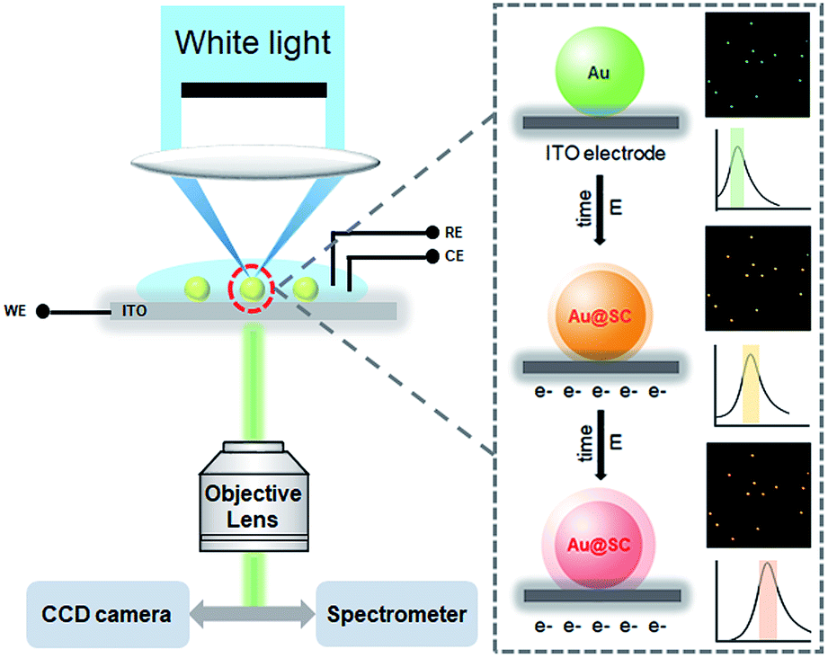 | ||
| Scheme 1 Experimental setup of the real-time dark-field imaging of in situ electrochemical synthesis of Au@SC core–shell NPs. | ||
Results and discussion
40 nm AuNPs were utilized as the core material for the synthesis of the core–shell photocatalysts. To form Au@CdS core–shell NPs, electrochemical deposition was performed using AuNPs modified ITO working electrodes. As previously reported, under pH lower than 2, S2O32− would be decomposed and form colloidal sulfur.32 Therefore, the electrodeposition reaction of CdS is dependent on pH. Here, in the coating of CdS, pH 3.0 H2SO4 solution was applied containing 0.1 M CdCl2 and 10 mM Na2S2O3 at room temperature. The deposition potential is selected from cyclic voltammetry (Fig. 1b). As illustrated in Fig. 1a, at potential lower than −0.8 V vs. Pt quasi-reference, S2O32− started to be reduced on the electrode to form S2−. Due to the strong affinity of Au atoms to sulfur,33,34 S2− ions were selectively adsorbed onto the surface of AuNPs. As shown in the cyclic voltammogram (Fig. 1b, red curve), Cd2+ was not directly reduced on the electrode, but reacted with S2− to form a CdS shell. The reaction mechanism of CdS deposition involves a 2-electron transfer which is as shown below.32,35,36| Cd2+ + S2O32− + 2e− → CdS + SO32− | (1) |
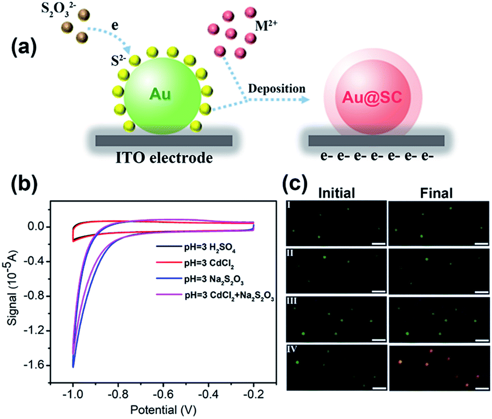 | ||
| Fig. 1 (a) Schematic diagram for the formation of the semiconductor shell on AuNPs. (b) Cyclic voltammograms of AuNPs modified ITO electrodes in pure pH = 3 H2SO4 (black curve), and containing 0.1 M CdCl2 (red curve), 0.01 M Na2S2O3 (blue curve), and 0.1 M CdCl2 and 0.01 M Na2S2O3 (purple curve), scan rate: 50 mV s−1. (c) Dark field images of AuNPs before and after chronoamperometry at −0.8 V (vs. Pt quasi-reference) in pure pH = 3 H2SO4 (I), and containing 0.1 M CdCl2 (II), 0.01 M Na2S2O3 (III), and 0.1 M CdCl2 and 0.01 M Na2S2O3 (IV) for 8 min (scale bar: 2 μm). | ||
The growth of shell was monitored using DFM and spectrometry in real time. As shown in Fig. 2, the 40 nm AuNP scattered a dark green spot with λmax centered at 558 nm according to the Lorentz fit. A true-color digital camera and electrochemical workstation were triggered simultaneously via a digital generator to monitor the synthesis of the core–shell nanostructure in real-time. Under a potential of −0.8 V (vs. Pt quasi-reference), the initial green spot turned brighter and generally changed to yellow and orange as time elapsed (Fig. 2c). The scattering band was recorded every minute. In 7 min, the scattering peak shifted from 558 nm to 598 nm with a significant intensity increase of 5.42-fold compared to the initial waveform. Meanwhile, the LSPR properties of Au@CdS with different shell thickness were analyzed using a finite-difference time domain (FDTD) method, which is a reliable technique in solving Maxwell’s equations in a dispersive medium.37 With a total field scattered-field source, theoretical simulation shows an obvious scattering peak red-shift from 550.336 nm to 601.342 nm (Fig. 2b) with 7 nm shell thickness increment, which exhibited the same trend as the experimental results. It should be noted that under the current status of the DFM platform we used, the scattering intensity of AuNPs with diameters smaller than 20 nm was too weak to be measured. We also examined the formation of Au@CdS core–shell NPs with 80 nm AuNPs. Fig. S1† displays the scattering spectra and images of a single 80 nm AuNP during the electrochemical growth of the CdS shell. Under a potential of −0.8 V (vs. Pt quasi-reference), the initial green-yellow spot turned brighter and generally changed to orange and red as time elapsed, with the scattering peak shifted from 580 nm to 640 nm in 9 min. The typical transmission electron microscopy (TEM) image verifies the formation of the CdS shell (Fig. S2†). Red and green are complementary colors with the highest contrast ratio. Therefore, for direct imaging analysis, the limitation of the AuNP core size could be 40–80 nm.
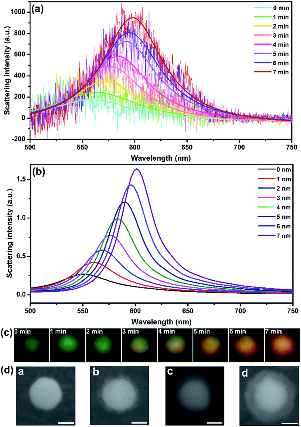 | ||
| Fig. 2 (a) Scattering spectra and Lorentz fit of an AuNP randomly selected during the electrochemical growth of the CdS shell. (b) Simulation results of scattering spectra response of Au@CdS with different shell thicknesses. (c) Dark-field images of a single particle during the electrochemical growth of the shell. (d) SEM images of 40 nm AuNP modified on ITO which undergoes different deposition times. (a): 0 min, (b): 3 min, (c): 6 min, (d): 9 min (scale bar: 20 nm). | ||
To determine the thickness of the shell during electrochemical deposition, scanning electron microscopy (SEM) is applied to in situ characterize the nanocomposites on ITO. In the nucleation stage, the SEM image can hardly distinguish the surface changes. An obvious core–shell structure was formed after 3 min under −0.8 V (vs. Pt quasi-reference), and the thickness was generally increased along with the increasing CdS deposition time. The shell thickness varied from 5 ± 2 nm, 9 ± 2 nm to 12 ± 2 nm corresponding to the electrodeposition time of 3, 6 and 9 min (Fig. 2d). The shell was getting more uniform along with increasing deposition time. Compared to the morphology study using an electron microscope, LSPR observed under DFM provides an in situ real-time imaging mode which is fast and direct. It should be noted that the scattering spectra as well as the dark field images were obtained from the same particle. However, for SEM characterization, the shell thicknesses on different particles are quite uniform. Therefore, the images in Fig. 2d were obtained from different particles.
The scattering color change and spectral shift could be used to monitor the kinetics of surface nucleation and growth. As the color of the spot changed synchronously with the scattering intensity and wavelength, we did color analysis by evaluating a series of images using ImageJ and extracted the red/green (R/G) value of each separate spot. As shown in Fig. 3, 19 spots in a visual field were analyzed. For all these spots, the R/G value increased along with the increasing deposition time from 0–8 min, indicating the successful formation of CdS on all these AuNPs. In addition, as the R/G values of different spots fluctuated in a small range at the same time, we could estimate uniform growth of CdS shells on all these particles. We have analyzed the relationship between the average shell thickness obtained from TEM and SEM images and the ΔR/G value, the fitted curve is illustrated in Fig. 3c. Mie theory verified that the LSPR wavelength shifts exhibited an exponential relationship with shell thickness.38 In this work, the estimated average shell thickness from SEM and TEM images also exhibited a good exponential fitting with the ΔR/G value, with the equation y = 2.35 − 2.35![[thin space (1/6-em)]](https://www.rsc.org/images/entities/char_2009.gif) exp(−0.06x). Further, we also correlated the shell thickness with the shift of the scattering spectra from Fig. 2a, and presented the results in Fig. S3.† Δλmax obtained from FDTD simulation, as well as the measured Δλmax from the scattering spectra exhibited good exponential fits with shell thickness.
exp(−0.06x). Further, we also correlated the shell thickness with the shift of the scattering spectra from Fig. 2a, and presented the results in Fig. S3.† Δλmax obtained from FDTD simulation, as well as the measured Δλmax from the scattering spectra exhibited good exponential fits with shell thickness.
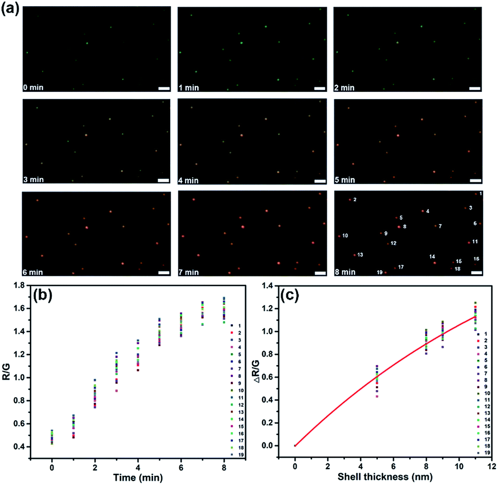 | ||
| Fig. 3 (a) Dark-field images of 19 particles in a visual field during the electrochemical deposition of CdS on AuNPs. (b) The R/G value variation of each particle with time elapsed (scale bar: 1 μm). (c) The estimated average shell thickness dependence upon the ΔR/G value; the data were fit to a line with the equation y = 2.35 − 2.35exp(−0.06x). | ||
To further characterize the obtained core–shell structure, the in situ formed Au@CdS NPs were separated from the ITO substrate using ultrasound. Fig. 4a and c show the TEM images of the composite nanocrystals. The apparent contrast between the inner core and the outer shell can be seen with the clear metal/semiconductor interface. After applying a deposition potential of −0.8 V (vs. Pt quasi-reference) for 5 min and 8 min, the shell thickness grew to about 8 nm and 11 nm. Both TEM (Fig. 4a, c and S4†) and SEM (Fig. 4b, d) images show that the obtained core–shell NPs have good homogeneity and dispersion. Also, we measured the shell thickness based on the TEM image (Fig. S5†), the result was similar to that from the SEM image (Fig. 2d). It is worth noting that CdS was rarely formed on ITO, which confirmed that Cd2+ was tending to react with S2− which adsorbed on the surface of AuNPs to form the CdS shell, instead of reducing on ITO. The composition within the core–shell particles was then examined using TEM-energy dispersive spectrometry (TEM-EDS). The TEM-EDS elemental mapping of Au, Cd and S shown in Fig. 4e confirmed the core–shell feature of the Au@CdS nanocrystals. An HRTEM image was taken at the interface of the core/shell region of a single particle (Fig. 4f). Interlayer spacings of 0.236 nm and 0.202 nm were observed in the core region, in good agreement with the d spacing of the (111) and (200) lattice planes of the fcc Au crystal.39 In the shell region, interlayer spacings of 0.335 nm and 0.353 nm was obtained, complying with the lattice spacings of the (002) and (100) planes of the wurtzite (hexagonal) crystal CdS (Fig. 4f and S6†).35,36,40 The abrupt transformation of the lattice arrangement across the interface implies no epitaxial relationship exists between Au and CdS. The lattice mismatches are about 32.86% and 30.65% according to the measured lattice spacing in Fig. S6a and b.† In addition, the X-ray diffraction (XRD) pattern of the Au@CdS NPs shown in Fig. S7† verifies the electrochemical deposition of hexagonal wurtzite CdS along with fcc Au nanocrystals, and the diffraction peak of CdS was more obvious with longer deposition time (Fig. S7a†).
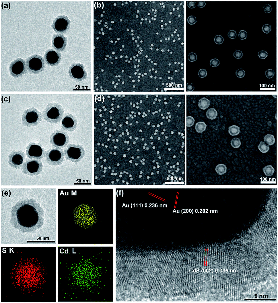 | ||
| Fig. 4 TEM (a and c) and SEM (b and d) images of AuNPs with application of −0.8 V (vs. Pt quasi-reference) for 5 and 8 min to form Au@CdS NPs. (e) EDX elemental mapping of Au@CdS NP. (f) HR-TEM image of Au@CdS NP. | ||
The electrochemical synthesis of Au@SC core–shell nanocrystals is practical and universal. We extended the method to synthesize Au@ZnS NPs and Au@CdSe NPs. Similar to the electrochemical deposition of Au@CdS, at a negative potential of −0.8 V (vs. Pt quasi-reference) in pH 4.0 H2SO4 solution containing 0.1 M ZnCl2 and 10 mM Na2S2O3, ZnS was formed as a shell on the surface of 40 nm AuNPs with highly uniform thickness, which was increased as time elapsed (Fig. S8†). It should be noted that the deposition of semiconductor shells proceeded faster in acidic solution with a lower pH value.32 The solubility-product constants (Ksp) of ZnS and CdS are about 1.2 × 10⁻²³ and 3.6 × 10⁻²⁹, respectively. As ZnS can be more easily dissolved in diluted acids compared to CdS, the pH value in the case of ZnS was set to be higher than that for CdS.41 The core–shell feature was further confirmed by elemental mapping (Fig. S9d†). As shown in the HRTEM image of the Au@ZnS structure (Fig. S9c†), hexagonal ZnS had d spacings of 0.331 and 0.196 nm, which was in agreement with the values of the (100) and (110) lattice planes formed on Au (111) planes (0.239 nm d spacing).42 The growth speed for the ZnS shell was about 37% lower than that of CdS, which could be ascribed to its lower association rate with S2−. Similar to the selective adsorption of S2− ions on the Au surface, Se2− shows strong affinity to Au atoms. And the formation of CdSe on Au nanocrystals was extremely fast. Cyclic voltammetry sweeping from −0.4 V to −0.8 V (vs. Ag/AgCl) with a scan rate of 100 mV s−1 for one cycle resulted in the formation of hexagonal CdSe on Au with a shell thickness of 5 ± 2 nm (Fig. S10†). The crystalline forms of ZnS and CdSe were further characterized by XRD (Fig. S7b and c†).
Further we demonstrated the photocatalytic hydrogen evolution performances of Au@CdS NPs with increased shell thickness using a N2-saturated aqueous solution containing 0.35 M Na2SO3 and 0.24 M Na2S under 532 nm laser to irradiate the LSPR of AuNPs. As shown in Fig. 5a, the Au@CdS NPs modified ITO exhibited prompt response to on/off cycles of light excitation. Compared to that of CdS NPs, Au@CdS core–shell structures show obviously larger photocurrents (Fig. S11†), which is attributed to the enhanced charge separation efficiency and increased electron–hole generation.43 Under light irradiation, the photoelectrons were generated and effectively involved in reducing H+ into H2. Meanwhile, the photo-induced holes could be consumed by Na2SO3 and Na2S, which served as the hole scavengers.44 It is obvious that along with the increase in shell thickness, the photocatalytic performance went through a sudden rise and fall process. Within 3 min deposition at a constant potential of −0.8 V, the photocurrent generation efficiencies of Au@CdS NPs on ITO increased and reach 74.4 μA cm−2 at 3 min (shell thickness: 4–7 nm), which was much higher than that obtained with longer deposition time. There are two possible reasons. On the one hand, the increase in shell thickness may affect the absorption of light which in turn affects the production of hot electrons. On the other hand, the increased distance of the hot electrons from the AuNPs to the shell would result in more recombination of electron and hole.45 Under DFM, it is the point that the color of the spots changes from green to yellow. We calculated the incident photon to current conversion efficiency (IPCE) using the equation below.
 | (2) |
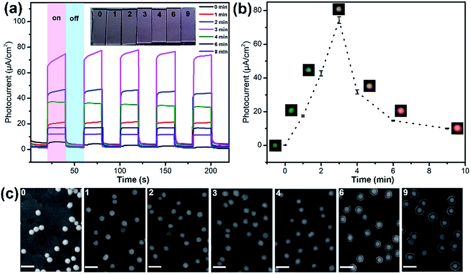 | ||
| Fig. 5 (a) Photocurrents of Au@CdS NPs modified ITOs irradiated with visible light of 532 nm at −0.3 V (vs. SCE) with electrodeposition times of 0 min, 1 min, 2 min, 3 min, 4 min, 6 min and 9 min. The inset picture shows the color changes of the ITO electrodes under different deposition times. (b) The relationship between photocurrent and electrochemical deposition time. (c) SEM images of Au@CdS NPs with different deposition times on ITO electrodes (scale bar: 100 nm). | ||
Conclusions
In summary, we report a proof-of-concept method to synthesise plasmonic photocatalysts with a core–shell structure via electrochemical deposition. Due to the strong affinity of Au atoms to S2− and Se2−, semiconductor shells of CdS, CdSe and ZnS were in situ formed on the surface of the Au core, which conquered the barrier caused by a large lattice mismatch between the two components. Besides the enhanced local electric field and heating effect, LSPR provides another opportunity, which is real-time imaging of the structure growth process. Under DFM, the scattering color, intensity or wavelength changes could be used to monitor the surface nucleation and growth. The whole synthesis and imaging processes could be carried out in aqueous solution under room temperature, which is practical, direct and fast. As a simple and universal technique, this system could be applied to cases with other metal cores. With the proposed method, plasmonic nanostructures with diverse composition, size and morphology could be obtained, which shows great opportunity in solar photocatalysis.Experimental
Chemicals and materials
40 nm AuNPs were purchased from Ted Pella, Inc, with surface stabilized by sodium citrate. Cadmium chloride (CdCl2), cadmium sulfate (CdSO4), zinc chloride (ZnCl2), selenium dioxide (SeO2), sodium thiosulfate (Na2S2O3), sulfuric acid (H2SO4), sodium sulfide (Na2S) and sodium sulfite (Na2SO3) were obtained from Sinopharm Chemical Reagent Co. Ltd. (3-Aminopropyl) triethoxysilane (APTES, 99%) was purchased from Sigma-Aldrich. Milli-Q water with resistivity >18 MΩ cm was used throughout all experiments.Experimental setup and data acquisition
Dark-field imaging was carried out on an inverted microscope (IX73, Olympus), which was equipped with a dark-field condenser (0.8 < NA < 0.92) and a 60× objective lens (NA = 0.7). The light source was a 100 W halogen lamp. White light collected by the objective was directed either into a true-color digital camera (Olympus DP80, Japan) or into the entrance of a slit of a monochromator (Acton SP2358,PI, USA) equipped with a grating (grating density, 300 lines per mm; blazed wavelength, 500 nm) and recorded by a liquid nitrogen cooled EMCCD (400BR, PI, USA) for scattering spectra acquisition. Scattering spectra were background corrected by subtracting and dividing by a background scattering spectrum taken from a nearby clean area on the sample. To determine the peak scattering wavelength, spectra were fitted with a Lorentzian function. HRTEM was performed with a JEM-2100 transmission electron microscope (JEOL Ltd., Japan). SEM images of nanoparticles on working electrodes before and after electrochemical growth were acquired using a Hitachi S4800 (JEOL Ltd., Japan) operating at beam voltages of 5–15 kV. X-ray diffraction (XRD, Bruker, D8 advance) was used to characterize the structures and components of samples with Cu Kα radiation (40 kV, 40 mA) and a scanning speed of 6 degrees per min.Surface modification of ITO electrodes
Transparent electrodes consisting of glass substrates coated with a 150 nm indium tin oxide (ITO) film were first boiled with a 2.0 M isopropyl alcohol solution of KOH for 15 min, then sequentially ultra-sounded in Milli-Q water, acetone, Milli-Q water, ethanol, and Milli-Q water for 10 min. Further, the slides were dried under a N2 flow. The thoroughly cleaned ITO electrodes were immersed into an ethanolic solution of APTES (1% v/v) overnight at room temperature, then washed sequentially with ethanol and ultrapure water three times, dried under a N2 flow, and finally baked in an oven at 120 °C for 3 h, thus the electrode surface was modified with amino groups. For dark field imaging, the AuNPs colloid was ten times diluted before use, then dropped 200 μL on ITO with PDMS hole (diameter 6 mm) for 1 min and washed with ultrapure water; the AuNPs with low density were randomly adsorbed on the ITO for dark field imaging. In order to obtain the synthesized nanoparticles for TEM and SEM characterization, a AuNPs stock solution was incubated on the amino modified ITO for 4 h, then washed thoroughly with ultrapure water. Because of electrostatic attraction, the gold nanoparticles were fixed on the electrode with a relatively high density. After electrochemical growth, these core–shell nanoparticles were removed from the ITO glass via ultrasonic treatment in 3.0 mL of ultrapure water for 30 s. The nanoparticles were centrifuged (9000 rpm, 5 min), washed with distilled water, and resuspended in 500 μL of aqueous solution for TEM characterization.Electrochemical deposition experiments
Electrochemical experiments were performed on a CHI 760 with a three-electrode system. For the formation of Au@CdS NPs, a AuNPs modified ITO electrode was used as the working electrode, and Pt wires (300 μm) were used as both counter and pseudoreference electrodes. The supporting electrolyte was pH = 3 H2SO4 solution containing 10 mM Na2S2O3 and 0.1 M CdCl2. We adopted chronoamperometry at a deposition potential of −0.8 V (vs. Pt) for 1–9 min. To form Au@ZnS NPs, the supporting electrolyte was pH = 4 H2SO4 solution containing 10 mM Na2S2O3 and 0.1 M ZnCl2. To form Au@CdSe NPs, the supporting electrolyte was 0.25 M H2SO4 with 14 mM SeO2 and 0.25 M CdSO4. The electrochemical deposition was performed with cyclic voltammetry, sweeping from −0.4 V to −0.8 V (vs. Ag/AgCl) at a sweep rate of 100 mV s−1 for one cycle. In addition, for the in situ deposition of CdS NPs on ITO, uncoated ITO was applied as the working electrode with deposition time of 10 min.Photocurrent measurements
A three electrode system was applied with ITO modified with Au@CdS NPs as the working electrode (effective working area: 0.1256 cm2), Pt as the counter electrode and SCE as the reference electrode. The electrolyte was N2-saturated 0.35 M Na2SO3 and 0.24 M Na2S aqueous solution. A fiber coupled laser (532 nm) with 400 μm diameter (laser out) was used in this experiment. The electrode with area of 0.1256 cm2 was exposed to the light, the power density at the electrode was measured to be 103.6 mW cm−2 using a laser power meter. The bias was set to be −0.3 V during the measurement.Theoretical modelling
Three-dimensional full-field finite-difference time domain (FDTD) (the package of Lumerical FDTD Solutions 8.15) method was used to perform the simulations about the optical properties of the core–shell NPs. The background was set with an ITO substrate, using a total-field scattered-field source, ranging from 500 to 800 nm, to investigate the scattering properties of the core–shell structure. The refractive index of CdS was set as 2.5.27,47Conflicts of interest
The authors declare no competing financial interest.Acknowledgements
This work was supported by the National Natural Science Foundation (Grants 21327902, 21535003, and 21605079) of China, and Excellent Research Program of Nanjing University (ZYJH004).References
- H. Tada, T. Mitsui, T. Kiyonaga, T. Akita and K. Tanaka, Nat. Mater., 2006, 5, 782–786 CrossRef CAS PubMed
.
- H. B. Yildiz, R. Tel-Vered and I. Willner, Adv. Funct. Mater., 2008, 18, 3497–3505 CrossRef CAS
- G. Oldfield, T. Ung and P. Mulvaney, Adv. Mater., 2000, 12, 1519–1522 CrossRef CAS
- T. Hirakawa and P. V. Kamat, Langmuir, 2004, 20, 5645–5647 CrossRef CAS PubMed
- M. Wang, M. Ye, J. Iocozzia, C. Lin and Z. Lin, Adv. Sci., 2016, 3, 1600024 CrossRef PubMed
- Y. Zhang, S. He, W. Guo, Y. Hu, J. Huang, J. R. Mulcahy and W. D. Wei, Chem. Rev., 2018, 118, 2927–2954 CrossRef CAS PubMed
- C. Clavero, Nat. Photonics, 2014, 8, 95–103 CrossRef CAS
- H. Yang, L.-Q. He, Y.-W. Hu, X. Lu, G.-R. Li, B. Liu, B. Ren, Y. Tong and P.-P. Fang, Angew. Chem., Int. Ed., 2015, 54, 11462–11466 CrossRef CAS PubMed
- C. M. Hill and S. Pan, J. Am. Chem. Soc., 2013, 135, 17250–17253 CrossRef CAS PubMed
- C. M. Hill, R. Bennett, C. Zhou, S. Street, J. Zheng and S. Pan, J. Phys. Chem. C, 2015, 119, 6760–6768 CrossRef CAS
- Y. Ma, A. L. Highsmith, C. M. Hill and S. Pan, J. Phys. Chem. C, 2018, 122, 18603–18614 CrossRef CAS
- Y. Ma, A. L. Highsmith and S. Pan, ECS Trans., 2018, 85, 1155–1162 CrossRef CAS
- Y. Wusimanjiang, Y. Ma, M. Lee and S. Pan, Electrochim. Acta, 2018, 269, 291–298 CrossRef CAS
- M. Chirea, S. S. E. Collins, X. Wei and P. Mulvaney, J. Phys. Chem. Lett., 2014, 5, 4331–4335 CrossRef CAS PubMed
- B. S. Hoener, S. R. Kirchner, T. S. Heiderscheit, S. S. E. Collins, W.-S. Chang, S. Link and C. F. Landes, Chem, 2018, 4, 1560–1585 CAS
- C. P. Byers, H. Zhang, D. F. Swearer, M. Yorulmaz, B. S. Hoener, D. Huang, A. Hoggard, W.-S. Chang, P. Mulvaney, E. Ringe, N. J. Halas, P. Nordlander, S. Link and C. F. Landes, Sci. Adv., 2015, 1, e1500988 CrossRef PubMed
- B. S. Hoener, C. P. Byers, T. S. Heiderscheit, A. S. D. S. Indrasekara, A. Hoggard, W.-S. Chang, S. Link and C. F. Landes, J. Phys. Chem. C, 2016, 120, 20604–20612 CrossRef CAS
- C. Schopf, A. Wahl, A. Martín, A. O’Riordan and D. Iacopino, J. Phys. Chem. C, 2016, 120, 19295–19301 CrossRef CAS
- K. Wonner, M. V. Evers and K. Tschulik, J. Am. Chem. Soc., 2018, 140, 12658–12661 CrossRef CAS PubMed
- C. Jing, F. J. Rawson, H. Zhou, X. Shi, W. H. Li, D. W. Li and Y. T. Long, Anal. Chem., 2014, 86, 5513–5518 CrossRef CAS PubMed
- C. Jing, Z. Gu, T. Xie and Y. T. Long, Chem. Sci., 2016, 7, 5347–5351 RSC
- Y. Liu and C. Z. Huang, ACS Nano, 2013, 7, 11026–11034 CrossRef CAS PubMed
- S. Sun, M. Gao, G. Lei, H. Zou, J. Ma and C. Huang, Nano Res., 2016, 9, 1125–1134 CrossRef CAS
- J. Zhou, T. Yang, W. He, Z. Y. Pan and C. Z. Huang, Nanoscale, 2018, 10, 12805–12812 RSC
- V. Subramanian, E. Wolf and P. V. Kamat, J. Phys. Chem. B, 2001, 105, 11439–11446 CrossRef CAS
- V. Subramanian, E. E. Wolf and P. V. Kamat, Langmuir, 2003, 19, 469–474 CrossRef CAS
- W.-T. Chen, T.-T. Yang and Y.-J. Hsu, Chem. Mater., 2008, 20, 7204–7206 CrossRef CAS
- M. Li, X.-F. Yu, S. Liang, X.-N. Peng, Z.-J. Yang, Y.-L. Wang and Q.-Q. Wang, Adv. Funct. Mater., 2011, 21, 1788–1794 CrossRef CAS
- L. Huang, J. Zheng, L. Huang, J. Liu, M. Ji, Y. Yao, M. Xu, J. Liu, J. Zhang and Y. Li, Chem. Mater., 2017, 29, 2355–2363 CrossRef CAS
- J. Zhang, Y. Tang, K. Lee and M. Ouyang, Science, 2010, 327, 1634–1638 CrossRef CAS PubMed
- C. Gu, H. Xu, M. Park and C. Shannon, Langmuir, 2009, 25, 410–414 CrossRef CAS PubMed
- F. Kadirgan, D. Mao, W. Song, T. Ohno and B. Mccandless, Turk. J. Chem., 2000, 24, 21–24 CAS
- C. X. Guo, J. Xie, H. Yang and C. M. Li, Adv. Sci., 2015, 2, 1500135 CrossRef PubMed
- X.-L. Yin, J. Liu, W.-J. Jiang, X. Zhang, J.-S. Hu and L.-J. Wan, Chem. Commun., 2015, 51, 13842–13845 RSC
- S. Banerjee, S. K. Mohapatra, P. P. Das and M. Misra, Chem. Mater., 2008, 20, 6784–6791 CrossRef CAS
- Z. Shao, W. Zhu, Z. Li, Q. Yang and G. Wang, J. Phys. Chem. C, 2012, 116, 2438–2442 CrossRef CAS
- K. S. Yee, IEEE Trans. Antennas Propag., 1966, 14, 302–307 Search PubMed
- M. D. Malinsky, K. L. Kelly, G. C. Schatz and R. P. Van Duyne, J. Am. Chem. Soc., 2001, 123, 1471–1482 CrossRef CAS
- Z. Fan, X. Zhang, J. Yang, X. J. Wu, Z. Liu, W. Huang and H. Zhang, J. Am. Chem. Soc., 2015, 137, 10910–10913 CrossRef CAS PubMed
- K. Yamaguchi, T. Yoshida, T. Sugiura and H. Minoura, J. Phys. Chem. B, 1998, 102, 9677–9686 CrossRef CAS
- H. M. M. N. Hennayaka and H. S. Lee, Thin Solid Films, 2013, 548, 86–90 CrossRef CAS
- J. Zhang, Y. Wang, J. Zhang, Z. Lin, F. Huang and J. Yu, ACS Appl. Mater. Interfaces, 2013, 5, 1031–1037 CrossRef CAS PubMed
- K. H. Leong, A. A. Aziz, L. C. Sim, P. Saravanan, M. Jang and D. Bahnemann, Beilstein J. Nanotechnol., 2018, 9, 628–648 CrossRef CAS PubMed
- X. Ma, K. Zhao, H. Tang, Y. Chen, C. Lu, W. Liu, Y. Gao, H. Zhao and Z. Tang, Small, 2014, 10, 4664–4670 CrossRef CAS PubMed
- S. T. Kochuveedu, Y. H. Jang and D. H. Kim, Chem. Soc. Rev., 2013, 42, 8467–8493 RSC
- L. Ma, K. Chen, F. Nan, J.-H. Wang, D.-J. Yang, L. Zhou and Q.-Q. Wang, Adv. Funct. Mater., 2016, 26, 6076–6083 CrossRef CAS
- S. Liang, J.-B. Li, M. Li and X. Tang, Plasmonics, 2018, 13, 181–187 CrossRef CAS
Footnotes |
| † Electronic supplementary information (ESI) available: Additional figures, additional results and discussion and details for digital simulation. See DOI: 10.1039/c9sc02804h |
| ‡ These authors contributed equally. |
| This journal is © The Royal Society of Chemistry 2019 |