
 Open Access Article
 This Open Access Article is licensed under a
 Creative Commons Attribution 3.0 Unported Licence
Double cascade dressed MOSFET from doped Eu3+and Pr3+ in a host YPO4
Huanrong Fana,
Al Imranb,
Faizan Razaa,
Irfan ahmedbc,
Kamran Amjada,
Peng Lia and
Yanpeng Zhang *a
*a
aKey Laboratory for Physical Electronics and Devices of the Ministry of Education, Shaanxi Key Lab of Information Photonic Techniques, Xi'an Jiaotong University, Xi'an 710049, China. E-mail: ypzhang@mail.xjtu.edu.cn
bDepartment of Physics, City University of Hong Kong, Hong Kong
cElectrical Engineering Department, Sukkur IBA, Sukkur 65200, Sindh, Pakistan
First published on 27th November 2019
Abstract
In this paper, we study double cascade dressed optical metal oxide semiconductor field-effect transistor (MOSFET) by exploiting enhancement and suppression for mixed-phase (hexagonal + tetragonal) of Eu3+:YPO4 and different phases (hexagonal + tetragonal and pure tetragonal) of Pr3+:YPO4 crystals. We report variation of fine structure energy levels in different doped ions (Eu3+ and Pr3+) in the host YPO crystal. We compared multi-level energy transition from a single dressing laser with single level energy transition from double cascade dressing lasers. Gate delay facilitates multi-energy level dressed transition and is modeled through a Hamiltonian. Based on the results of double cascade dressing, we have realized MOSFET for logic gates (inverter and logic not and gate) with a switching contrast of about 92% using a mixed phase of Pr3+:YPO4.
Introduction
In the last few decades, scientists have shown increased interest in widening the knowledge of rare earth ions doped in crystals due to the potential applications in optical devices1–5 and quantum computing.6 Since Eu3+ and Pr3+ ions are more sensitive to the site symmetry and its surrounding crystal-field of the host material than other crystal ions,7,8 it can be achievable to get such kinds of potential application in YPO4 crystals. The crystal structure of YPO4 has two polymorphic forms, tetragonal (T-) and hexahedral (H-) phases.9–12 The slight variation of local structure will bring significant changes in the optical properties.In theory, the tetragonal (T) phase of crystal is more structurally symmetric than the hexahedral (H) phase in Eu3+ and Pr3+ ions because of a more atomic-like system.13 In our experiment, a mixed contribution of T phase (more) + H phase (less) of crystal at low power performed better because of good transmission of information for the crystal T phase. The atomic density has a great influence on the number of splitting, which is relative to the dressing effect in atomic-like media.14,15 The observation of Autler–Townes (AT) splitting effect of FL spectrum induced by self or external fields and the polarization dependence of FL signals in Pr3+:Y2SiO5 has been reported.16 Wen et al., realized optical switch and amplifier from dressing suppression and enhancement inmulti-order fluorescence (FL) and spontaneous parametric four-wave mixing (SP-FWM) in Pr3+:Y2SiO5.17 Controlled correlation and squeezing in Pr3+:Y2SiO5 to yield correlated light beams has also been investigated.18 Transition between the bright and dark states can modify the non-linear behaviour of crystal on singly- and doubly-dressed four-wave-mixing (FWM) processes.19 Diamond nitrogen-vacancy (NV) center were studied to realize optical transistors and hybrid switch.20,21 Eu3+:YPO4 and Pr3+:YPO4 crystals have been configured to observe second-order FL signals.
In this paper, we study the energy level transition of europium doped YPO (Eu3+:YPO4) and praseodymium doped YPO (Pr3+:YPO4) crystals with different phases using dressing lasers. By changing different parameters of single and double laser (power, detuning, and gate delay), we observed the dressed energy level transition from single to multi-level with a single laser; and single-level using double laser. Each sample responded based on their ions structure and phase symmetry in the host YPO crystal. In contrast to single multi-level dressing, double cascade dressed single level energy transition outputs are robust and are observed to be of special interest because of half peak with half suppression dip. These kinds of results are very important for realizing metal oxide semiconductor field-effect transistor (MOSFET).
Basic theory
In this experiment, both samples were held separately during the experiment running in a cryostat (CFM-102) with a temperature of 77 K. Fig. 1(a) shows a fine structure and a hyperfine structure of host material YPO4. The Eu3+:YPO4 has two states, named ground state 7F1 and excited state 5D0. Under the action of the crystal field of YPO4, the ground state 7F1 is split, which is fine-structure levels. Fig. 1(b) shows the simplified energy-level diagram of Eu3+ doped YPO4 (Eu3+:YPO4) and Pr3+ doped YPO4 (Pr3+:YPO4) crystal. Fig. 1(c) shows the schematic diagram of the experimental setup. Two dye lasers (narrow scan with a 0.04 cm−1 line width) are pumped by an injection-locked single-mode Nd:YAG laser (Continuum Powerlite DLS 9010, 10 Hz repetition rate, 5 ns pulse width), which are used to generate the pumping fields E1 (ω1, Δ1) and E2 (ω2, Δ2) with frequency detuning of Δi = Ωmn − ωi, where Ωmn is the corresponding atomic transition frequency between levels |m〉〉 and |n〉. ωi (i = 1, 2) is the laser frequency. Arrangements of two photomultiplier tubes (PMT1-2) are used to detect the generated Stokes (ES), anti-Stokes (EAS), and FL composite signals (Fig. 1(c)). The pumping field Ei (where i = 1, 2) excites the sample and is reflected field from the surface of Eu3+:YPO4 into its original with a small angle θ between them. The spectral signals are obtained by scanning laser frequency, while time-domain signals are obtained by fixing laser frequency. Fig. 1(d) and (e) show dressed energy level, through which SP-FWM process configured in the lambda level system. Fig. 1(e) SP-FWM in a two-level system.
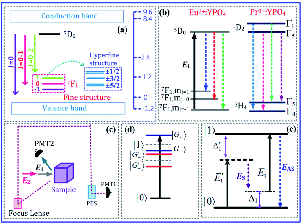 | ||
| Fig. 1 (a) Fine and hyperfine energy level of Eu3+:YPO4. (b) Energy level diagram of Eu3+:YPO4 and Pr3+:YPO4.22–24 (c) Schematic diagram of experimental setup. (d) Four-wave mixing (FWM) of lambda level system. (e) FWM in a two-level system. | ||
In Fig. 1(e), the density matrix of the FL via perturbation chain 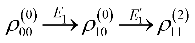 can be written as
| ρ(2)11 = −|G1|2/[(d1 + |G1|2/Γ00)(Γ11 + |G1|2/d1)], | (1) |
 and
and 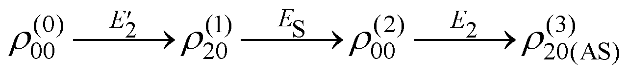 , respectively, can be written as
 | (2) |
 | (3) |
The lifetime of the Stokes/anti-Stokes signal can be written as ΓS/AS = Γ00 + 2Γ20.
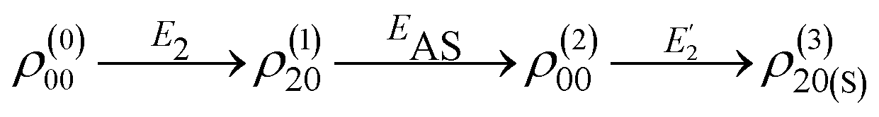
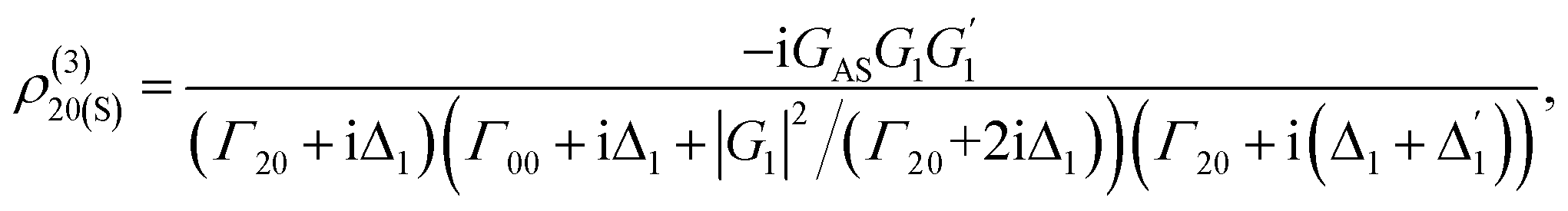
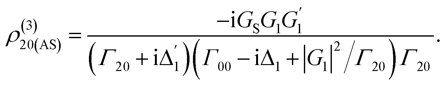
In Λ-type three-level system(shown in Fig. 4(c)), taking into account the self-dressing effect of E1 and the external-dressing field E2, the third-order nonlinear density matrix elements of ES and EAS are given by 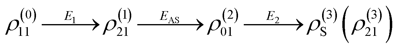 and
and 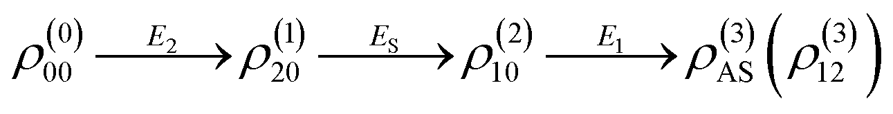 , respectively. The dressed density matrix elements, in this case, are given as follows
 | (4) |
 | (5) |
The lifetime of the Stokes/anti-Stokes signal can be written as ΓAS = Γ10 + 2Γ20. Similarly, fourth-order FL ρ(4)FL in Λ-type system via the pathway  is
is
| ρ(4)FL = −|G1|2/[(Γ21 + iΔ1)(Γ22 + |G1|2/(Γ01 − iΔ1) + |G2|2/(Γ20 + iΔ2))]. | (6) |
Therefore, the intensity of the measured FL signal can be described as
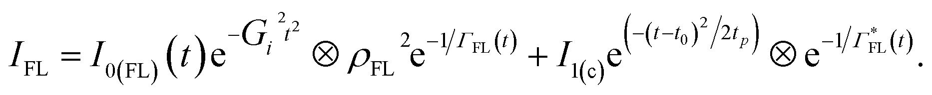 | (7) |
Owing to the interaction of the coupling field, the homogeneous linewidth broadening of the measured for FL is given as
| Γi/j = Γpop + Γion–spin + Γion–ion + Γphonon − Γdressing. | (8) |
Experimental results and discussion
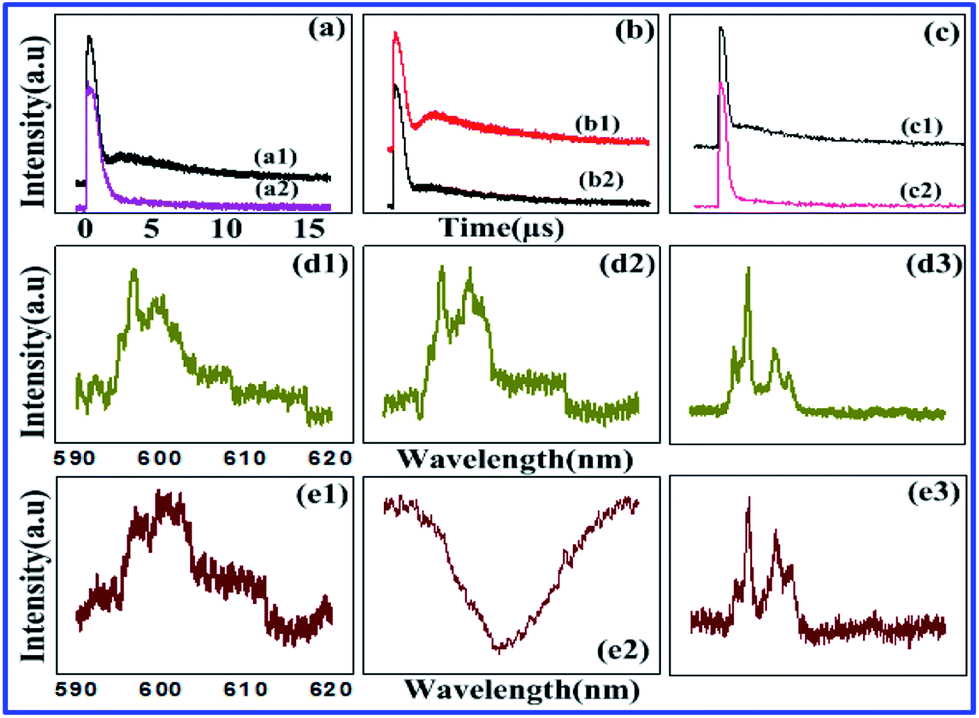
Fig. 2(a1–a4) and (b1–b4) show spectral intensities of output signals observed at PMT2 and PMT1 (confocal detector), respectively, form a mixed phase of Eu3+:YPO4. The intensities displayed from Fig. 2(a1 and b1)–(a4 and b4) are recorded by gate delay at 200 ns, 2 μs, 10 μs, and 2 ms, respectively. Change in gate delay is demonstrated in Fig. 2(c) and (d); corresponds to change in different energy levels of Fig. 2(a) and (b). The bright to dark states are shown in Fig. 2(e) for illustration purpose based on single laser and single-level dressing. In Fig. 2(a1 and a3), the spectral signal recorded at PMT2 is composed of second-order FL (ρ(2)11) and SP-FWM (ρ(3)10(S/AS)), thus making a compo site signal (ρ(2)11 + ρ(3)S) at PMT2. Composite signal is by produced E1 and
  along with FL at PMT2, and Fig. 2(b1) is similar to PMT1. In comparison with Fig. 2(a1), FL dominates in Fig. 2(b1) due to the focused detection. Physically, Hamiltonian is at |1〉 a frequency reference point (dark state) in Fig. 2(e). Using this equation of Hamiltonian H|G1±〉 = λ±|G1±〉, one can get the split energy level
 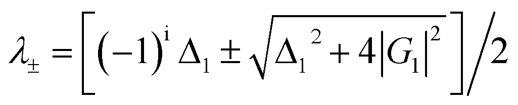 . When gate delay is changed from 200 ns to 2 μs, the dip appears in Fig. 2(a2) due to dressed suppression conditions Δ1 = 0of (|G1|2/d3) from eqn (2). When the gate delay is at 2 μs and 10 μs, the dip also appears in Fig. 2(b2 and b3). This phenomenon can be explained by E1 falling on dark states, which splits into two bright states (|G1+〉 and |G1−〉) and one dark state (|1〉), likewise the case in Fig. 2(a2). Signal linewidth is decreased from gate delay 200 ns to 10 μs. in Fig. 2(a1 and a3) due to SP-FWM ρ(3)S in ρ(2)11 + ρ(3)S. At the gate delay of 2 ms, the intensity of the spectral signal is decreased. So, only the intensity noise signal is obtained in Fig. 2(a4). The single dressing effect of E1 is different at PMT1 or PMT2 by changing gate delay at medium power. Comparing recorded spectral intensities at PMT1 and PMT2, PMT1 has more FL due to detection through confocal lens, demonstrating broader line width and relatively obvious single laser dressing.
 | ||
| Fig. 2 (a1–a4) Shows spectral intensity observed from a mixed phase of Eu3+ (more tetragonal and less hexagonal) doped in YPO at different gate delays and with fixed E1 at 4 mW while scanned from 575 nm to 610 nm. (b1–b4) Shows the same as (a1–a4), respectively, but the spectral signal, in this case, is routed through confocal lens to PMT (confocal detector). (c) and (d) Connecting diagram for PMT2 and confocal PMT1 corresponding to (a) and (b), respectively. (e) Energy level diagram for a single laser. (f) Schematic diagram of the MOSFET logic “not” gate. | ||
Here, an optical MOSFET based logic inverter or “not” gate has been realized through the results of Fig. 2(a) and (b). The model of the MOSFET logic inverter gate is shown in Fig. 2(f), where E1 is input signal (analogous to the gate voltage and gate current of MOSFET) and Y is the output of the MOSFET. To realize the logic inverter or not gate function of the MOSFET, when the input of the MOSFET E1 performs off-state, the output of the MOSFET Y performs on-state as a spectral peak in Fig. 2(a1) and (a3) (likewise Fig. 2(f1)). Here in Fig. 2(a1) and (a3), the output of the MOSFET Y satisfies the logical output condition 1. The spectral intensity of output spectral signal (off-states) in Fig. 2(a2) responses like MOSFET inverter as a suppression dip (Fig. 2(f2)). The MOSFET inverter as a suppression dip performs off state in Fig. 2(a2) (likewise Fig. 2(f2)), and it satisfies the output Y of the MOSFET inverter with logical 0 condition. The logic inverter or not gate contrast can be defined as C = (Ioff − Ion)/(Ioff + Ion), where Ioff is the light intensity at the off-state and Ion is the light intensity at the on-state. The switching contrast C is about 75% from Fig. 2(a2)–(a3). Compared with Fig. 2(a2)–(a3), the logic inverter, or not gate contrast in Fig. 2(b1)–(b2) is similar, and the contrast is almost 78% from Fig. 2(b1)–(b2). The speed of the MOSFET inverter gate is 3 μs and 12 ns from Fig. 2(a1)–(a2) and from Fig. 2(b1)–(b2), respectively.
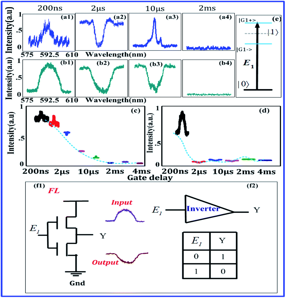
Fig. 3(a1–a4) and (b1–b4) shows spectral intensities of output signals measured at PMT2, when E1 is fixed at low power (1 mW) and high power (8 mW), respectively. Signal linewidth is also decreased from gate delays of 200 ns to 20 μs in Fig. 3(a1, a3) and (b1, b4) due to ρ(3)S. But signal linewidth in Fig. 3(b1–b4) at 8 mW is wider than that of in Fig. 3(a1–a4) at 1 mW due to multi-energy level dressed split at higher power by single dressing laser (Fig. 3(e)). However, at focused PMT1, the FL demonstrated the robust behaviour affected by dressing laser and gate delay dependency of multi-energy levels. It should be noted that the multi-level energy splitting is caused by E1 only, whereas, higher gate delay act as assisting to dressing parameter, which opens up a window for multi-energy level dressing, causing splitting as the two phases are closely packed in mixed-phase symmetry of Eu3+:YPO4. In principle, gate delay facilitates E1 field dressing, which excites (|1〉 and |2〉) and splits them into four bright states and two dark states, as illustrated in Fig. 3(e). In comparison with Fig. 2(e), two dark states |1〉 and |2〉 in Fig. 3(e) are different from one dark state |1〉. So one can say that |G1±〉 of |1〉 and |G1±〉 of |2〉form four bright states from a single dressing E1 when facilitated by gate delay. Physically, when the laser power of E1 is high, dressing |G1|2/d1 is increased suggested by eqn (1). By looking at Fig. 3(b3) at 20 μs, one can say laser dressing is assisted by gate delay to produce one small sharp peak, which comes by combining bright states (|G1−〉 of |1〉 and |G1+〉 of |2〉), and two dips (|1〉 and |2〉) from Fig. 3(e). One dip is shown in Fig. 3(a2 and b2), this phenomenon can be explained likewise Fig. 2(a2, b2 and b3). The interpretation of this peak in Fig. 3(a1, a3, b1 and b4) is same as in Fig. 2(a1, a3 and b1). Therefore, when the gate delay is increased at low power, the single dressing appears in Fig. 3(a3). At high power, dressing assisted by gate delay shows in Fig. 3(b2 and b3).
 | ||
| Fig. 3 (a1–a4) and (b1–b4) Show spectral signal of Eu3+:YPO4 (more tetragonal and less hexagonal) from detector 2 at low 1 mW and high 8 mW respectively, with different gate delays of 200 ns, 2 μs, 20 μs and 5 ms at 77 K. (c and d) Shows the same as (c) and (d), respectively, but at power of laser field changed to 8 mW. (e) Shows the multi-energy level diagram for two single individual dressing from a single laser beam. | ||
The MOSFET logic inverter or not gate performs on state, and it satisfies the output Y of the MOSFET inverter's logic 1 condition in Fig. 3(a1) and (b1). The output of the MOSFET Y performs off-state when it satisfies the logical output 0 condition in Fig. 3(a2) and (b2). So, MOSFET logic inverter or not gate is realized from Fig. 3(a1)–(a2) and from Fig. 3(b1)–(b2), where the inverter contrast C is about 72% and 80%, respectively.
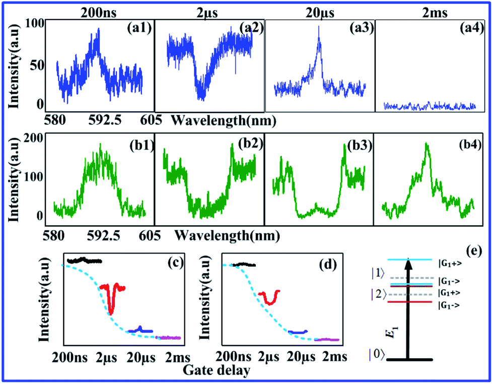
In Fig. 4(a1–a4), when gate delay is changed to 600 μs from 200 μs, the effect of double cascade dressing of E1 and E2 is getting obvious in Fig. 4(a2 and a4). The double dressing of E1 and E2 fall in dark states, which splits into three bright states (|G1+〉, |G2−+〉 and |G2−−〉) demonstrating three visible peaks and two dark state (|1〉, |G1−〉) corresponding to two dips in Fig. 4(a2 and a4), as suggested by Fig. 4(d). These dips and peaks are suggested by double cascade dressing |G1|2/(Γ01 − iΔ1) + |G2|2/(Γ00 + iΔ2) due to dressing suppression conditions Δ1 = 0, Δ2 = G1 from eqn (6). Fig. 4(a1 and a3) shows that by increasing gate delay from 200 ns to 2 μs AT splitting area varies from plan to deep. As dressing E1 plays a major role in Fig. 4(a1), while dressing E1 plays more role than dressing E2 in Fig. 4(a3). In Fig. 4(b1–b7), when E1 (594.8 nm) is shined by changing power from 2 mW to 8 mW and scanning E2 from 570–610 nm with 8 mW of power, similar trend of three visible peaks and two dips are gradually observed from Fig. 4(b6 and b7). AT splitting area varies from plan to deep by increasing power from 3 mW to 6 mW. The more obvious dressed energy level appears in Fig. 4(b2–b5) due to dressing E2 of high power. Comparing these two phenomenon of obtaining SP-FWM from suppressed dip of FL using gate delay in Fig. 4(a1–a5) and changing powers in Fig. 4(b1–b7), one can find the stronger double cascade dressing with more tetragonal and less hexagonal phase of Eu3+:YPO4 at 20 μs due to symmetry in Fig. 4(b6 and b7). Dressing effect of E1 and E2 in terms of AT splitting is obvious by changing gate delay and power in Eu3+:YPO4. Therefore one can characterize such a phenomenon obtained in Fig. 2(a2, b2 and b3), Fig. 3(b3) and Fig. 4(a2, b6 and b7) as single dressing, multi-energy level dressing by single laser assisted by gate delay and double cascade dressing in Eu3+:YPO4, respectively.
 | ||
| Fig. 4 (a1–a5) Shows the spectral intensity recorded from a mixed phase of more tetragonal and less hexagonal Eu3+:YPO4 focused PMT1 by employing E1 and E2 at 77 K with gate delays of 200 ns, 600 ns, 2 μs, 20 μs, and 2 ms, respectively and at 8 mW of E2. (b1–b7) Shows the same recorded signal by changing E1 power from 2 mW to 8 mW while scanning E2 from 570–610 nm. (c) Lambda level system. (d) The energy level for double cascade dressing. (e) Schematic diagram of the NAND gate. | ||
Here, we have realized the optical logic NAND gate. The model of optical logic NAND gate is shown in Fig. 4(e). When E1 power is 2 mW, the intensity input spectral signal satisfies the logical condition (0,0) of the NAND gate, so the output spectral signal performs as on state (logical output 1) in Fig. 4(b1). When E1 power is increasing gradually from 2 mW to 4 mW, output spectral signals perform as on state in Fig. 4(b2–b3) and here, the input condition of a logical NAND gate can be (0,1) and (1,0) for realization. When E1 power is 6 mW, the intensity output spectral signal satisfies the logical input condition (1,1) of the NAND gate, and the output spectral signal performs as an off state (logical output 0) in Fig. 4(b5). Our experiment results are defined on state and off state by the NAND gate contrast, respectively inverter contrast. Here, C is 86% from Fig. 4(b1–b3) to (b5).
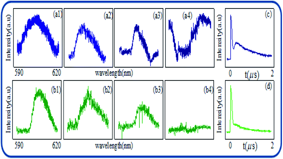
In Fig. 5(a1), the time-domain signal has little adiabatic population than Fig. 5(a2), because of double cascade dressing from E1 and E2. At resonant excitation in Fig. 5(b1 and b2), one can say that the adiabatic population is maximum at a resonant point in Fig. 5(b1) and comparatively less in Fig. 5(b2) because of a single dressing of E2. By looking at Fig. 5(c1 and c2), less adiabatic expansion has found for resonant and off-resonant E1 at 77 K. Signal linewidth is also decreased from the gate position 500 ns to 5 μs in Fig. 5(d1 and d3) or (e1 and e3) due to stokes of SP-FWM ρ(3)S. In the crystal field of YPO4:Pr3+, the (2J + 1) degeneracy is partly split, and the J = 0, 1, 2, 3, 4, 5, 6 levels split into 1, 2, 4, 5, 7, 8, 10 irreducible representations, respectively. Under this symmetry (1D2 and 3H4), two transition levels are allowed.19 Fig. 5(e2) shows double cascade dressing at low power due to dressing suppression conditions Δ1 = 0, Δ2 = 0 from eqn (6). Double cascade dressing of E1 and E2 is more obvious than that of E1 at low power or even by changing gate delay in Pr3+:YPO4. By comparing Pr3+ and Eu3+, at low power, the double cascade dressing effect in Pr3+:YPO4 (in Fig. 5(e2)) is stronger than Eu3+:YPO4 (in Fig. 4(b2)).
 | ||
| Fig. 5 (a) Shows the temporal intensity obtained from pure tetragonal phase of Pr3+:YPO4 at 600 nm, recorded from PMT2 by keeping (a1) E1, E2 and (a2) E2 laser beam at 1 mW at 77 K. (b1 and b2) Shows the same as (a1 and a2), respectively, but at resonant (596.8 nm) excitation. (c) Same signal obtained through (c1) resonant excitation of E1 and (c2) Off-resonance (590 nm) excitation of E1. (d1–d3) shows spectral intensity from Pr3+:YPO4 at different gate position 500 ns, 1.5 μs and 5 μs, with single E1 and (e1–e3) both E1 and E2. | ||
Here in Fig. 5, optical logic NAND gate has been realized, respectively Fig. 4. In Fig. 5(e1), spectral signal performs output on state (logical output 1) from the input logical (0,0) condition of optical logic NAND gate, as shown in the model in Fig. 4(e). In Fig. 5(e2), spectral signal performs output off state (logical output 1), and it can satisfy the input logical (1,1) condition of optical logic NAND gate, as shown in the model in Fig. 4(e). Here, contrast C is 88% (from Fig. 5(e1)–(e2)) as gate delay changed from 1 μs to 1.5 μs.
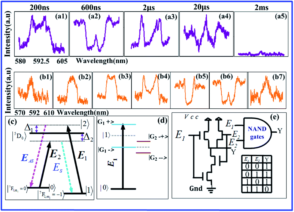
Fig. 6(a1–a4) shows the gradual and bit weak trend of the FL signal. By comparing Fig. 5 and 6 at low power, one can say that dressing effects observed in the tetragonal phase and mixed-phase (less tetragonal with more hexahedral) of Pr3+:YPO4 are different, which can be explained from different site symmetry. Here, we have realized the optical logic NAND gate. When output spectral signals are obtained at gate delays 200 ns, 600 ns, and 1 μs at low power of E1 and E2 in Fig. 6(a1–a3), spectral signals are performed as output on state (output 1) of the optical logical NAND gate. For realizing the output logical NAND gate, input conditions can be (0,0), (0,1) and (1,0) respectively Fig. 6(a1–a3). When output spectral signal is at gate delay 1.5 μs at low power of E1 and E2 in Fig. 6(a4), NAND gate performs off state (output 0) and it can satisfy the input condition of logical (1,1) for the NAND gate. Our experiment result defined the NAND gate contrast as C is 92% as gate delay changed from 200 ns to 1.5 μs in Fig. 6(a1) and (a4).
 | ||
| Fig. 6 (a1–a4) Shows the spectral intensity observed from mixed phase of Pr3+ (less tetragonal and more hexahedral) doped in YPO4 crystal at 77 K, recorded at PMT2 by changing gate delay from 200 ns, 600 ns, 1 μs and to 1.5 μs, respectively, and keeping E1 and E2 at low power 1 mW. (b1–b4) Shows the spectral intensity of the observed signal at PMT1 by changing gate delay and keeping the power of E1 at 1 mW. (c) and (d) Shows the time domain signal corresponding to (a) and (b), respectively. | ||
Conclusions
In summary, we demonstrated and compared single dressing based multi-level energy dressing assisted by gate delay and double cascade dressing based single energy-level transition in Eu3+:YPO4 and Pr3+:YPO4 crystals. We observed that at low power, a single dressing effect in Pr3+:YPO4 was stronger than Eu3+:YPO4, while the double cascade dressing effect was stronger in Eu3+:YPO4. Based on the outputs, logic gates (inverter and logic not and (NAND) gate) were realized by gate delay and power of laser fields. Such a detailed comparison of Eu3+ and Pr3+ doped in YPO4 can be of potential utility in nonlinear and quantum optics for quantum gates.Conflicts of interest
There are no conflicts to declare.Acknowledgements
This work was supported by the National Key R&D Program of China (2017YFA0303700, 2018YFA0307500), National Natural Science Foundation of China (61975159, 61605154, 11604256, 11804267, 11904279), and NSF of Shaanxi Province (2016JM6029).References
- M. N. Luwang, R. S. Ningthoujam, S. K. Srivastava and R. K. Vatsa, J. Mater. Chem., 2011, 21, 5326 RSC.
- A. V. Turukhin, V. S. Sudarshanam, M. S. Shahriar, J. A. Musser, B. S. Ham and P. R. Hemmer, Phys. Rev. Lett., 2001, 88, 023602 CrossRef.
- F. Beil, J. Klein, G. Nikoghosyan and T. Halfmann, J. Phys. B: At., Mol. Opt. Phys., 2008, 41, 074001 CrossRef.
- H. H. Wang, A. J. Li, D. M. Du, Y. F. Fan, L. Wang, Z. H. Kang, Y. Jiang, J. H. Wu and J. Y. Gao, Appl. Phys. Lett., 2008, 93, 221112 CrossRef.
- M. Sabooni, Q. Li, L. Rippe, R. K. Mohan and S. Kröll, Phys. Rev. Lett., 2013, 111, 183602 CrossRef PubMed.
- J. L. O'brien and L. Jeremy, Science, 2007, 318, 1567–1570 CrossRef PubMed.
- Z. Yahiaoui, M. A. Hassairi and M. Dammak, ýJ. Electron. Mater., 2017, 46, 8 Search PubMed.
- C. Li, L. Wang, H. Zheng, H. Lan, C. Lei, D. Zhang, M. Xiao and Y. P. Zhang, Appl. Phys. Lett., 2014, 104, 051912 CrossRef.
- P. Li, Y. Zhang, L. Zhang, F. Li, Y. Guo, Y. Li and W. Gao, Cryst. Growth Des., 2017, 17(11), 5935–5944 CrossRef CAS.
- Y. Hikichi, T. Sasaki, K. Murayama and T. Nomura, J. Am. Ceram. Soc., 1989, 72(6), 1073–1076 CrossRef CAS.
- M. N. Luwang, R. S. Ningthoujam, Jagannath, S. K. Srivastava and R. K. Vatsa, J. Am. Chem. Soc., 2010, 132(8), 2759–2768 CrossRef CAS PubMed.
- M. N. Luwang, R. S. Ningthoujam, S. K. Srivastava and R. K. Vatsa, J. Am. Chem. Soc., 2011, 133(9), 2998–3004 CrossRef CAS PubMed.
- P. Li, Y. P. Zhang, L. Zhang, F. Li, Y. X. Guo, Y. H. Li and W. P. Gao, Cryst. Growth Des., 2017, 11, 5935–5944 CrossRef.
- M. Fleischhauer and A. Imamoglu, Rev. Mod. Phys., 2005, 77, 633 CrossRef CAS.
- H. Wang, D. Goorskey and M. Xiao, Phys. Rev. Lett., 2001, 87, 073601 CrossRef CAS PubMed.
- D. Zhang, H. Y. Lan, C. B. Li, H. B. Zheng, C. J. Lei, R. M. Wang, I. Metlo and Y. P. Zhang, J. Phys. Chem. C, 2014, 118, 14521–14527 CrossRef CAS.
- F. Wen, I. Ali, A. Hasan, C. B. Li, H. J. Tang, Y. F. Zhang and Y. P. Zhang, Opt. Lett., 2015, 40, 20 Search PubMed.
- C. B. Li, Z. H. Jiang, Y. Y. Zhang, Z. Y. Zhang, F. Wen, H. X. Chen, Y. P. Zhang and M. Xiao, Phys. Rev. Appl., 2017, 7, 014023 CrossRef.
- Z. Q. Nie, H. B. Zheng, P. Z. Li, Y. M. Yang, Y. P. Zhang and M. Xiao, Phys. Rev. A, 2008, 77, 063829 CrossRef.
- N. Ahmed, G. A. Khan, R. Wang, J. G. Hou, R. Gong, L. M. Yang and Y. P. Zhang, Opt. Lett., 2017, 42, 9 CrossRef PubMed.
- F. Raza, A. Imran, A. Khan, H. Ullah, S. Zhang, S. Xiong, I. Ahmed and Y. P. Zhang, IEEE Photonics J., 2019, 11, 1–10 Search PubMed.
- O. K. Moune, M. D. Faucher and N. Edelstein, J. Lumin., 2002, 96, 51–68 CrossRef CAS.
- O. K. Moune, M. D. Faucher and N. Edelstein, J. Alloys Compd., 2001, 323–324, 783–787 CrossRef CAS.
- J. Collins, M. Geen, M. Bettinelli and B. D. Bartolo, J. Lumin., 2012, 132, 2626–2633 CrossRef CAS.
| This journal is © The Royal Society of Chemistry 2019 |