
 Open Access Article
 This Open Access Article is licensed under a Creative Commons Attribution-Non Commercial 3.0 Unported Licence
Quasiparticle effects on the linear and nonlinear susceptibility of ZnGeP2†
Hua Xie a,
Shenghao Fangb,
He Zhaoa,
Xiaoliang Xu*a,
Ning Ye*b and
Wei Zhuang*c
a,
Shenghao Fangb,
He Zhaoa,
Xiaoliang Xu*a,
Ning Ye*b and
Wei Zhuang*c
aKey Laboratory of Strongly-Coupled Quantum Matter Physics, Chinese Academy of Sciences, School of Physical Sciences, University of Science and Technology of China, Jinzhai Road 96, Hefei, Anhui 230026, P. R. China. Tel: +86-551-63607574
bKey Laboratory of Optoelectronic Materials Chemistry and Physics, Fujian Institute of Research on the Structure of Matter, Chinese Academy of Sciences, Fuzhou, Fujian 350002, China
cState Key Laboratory of Structural Chemistry, Fujian Institute of Research on the Structure of Matter, Chinese Academy of Sciences, Fuzhou, Fujian 350002, China. E-mail: wzhuang@fjirsm.ac.cn
First published on 4th November 2019
Abstract
The semiconductor zinc germanium diphosphide (ZnGeP2) has wide applications in the infrared nonlinear optics (NLO) due to its high nonlinear optical coefficient, wide infrared transparency range and high thermal conductivity. Absorptions near the pump or generation wavelength limit the effectiveness of this materials, with their complicated microscopic origins remaining largely elusive. Most research on the absorption mechanism of ZnGeP2 focused on the defect effect, while the quasi-particle effect and exciton effect are significant as well. We herein carried out the ab initio studies of the electronic band structure and optical properties of ZnGeP2 crystal. The quasiparticle and excitonic effects were examined by comparing the results of PBE, GW approximation and Bethe–Salpeter equation. Quasiparticle effect was found to widen the quasi-direct band gap and increases the valence and conduction band dispersions, which mainly blue-shifts the imaginary part of the dielectric function. The increased band gap also leads to a broadened lineshape in the second order susceptibility. The excitonic effects significantly enhance the peak intensity in the long wave regime of the dielectric function and red-shift the peaks in the high energy regime, leading to the greatly improved agreement with experiment. Our results provided a microscopic guidance for improving ZnGeP2's optical performance.
Introduction
Zinc germanium diphosphide (ZnGeP2) is one of the most extensively used nonlinear optical material for mid-infrared frequency conversion1–5 due to its large nonlinear coefficient (d36 = 75 pm V−1), high thermal conductivity (35 W mK−1), high damage threshold (1–2 J cm−2) as well as its low absorption coefficient (0.1 cm−1) in the spectral range of 2.5–8.3 μm.5,6 The as-grown ZnGeP2 presents the residual optical absorptions near the pump or generation wavelength, which reduce the optical-to-optical efficiency and raises the crystal elevated temperature. These thermo-optical effects result in the thermal lensing,7 which degrades the OPO beam quality considerably and therefore limits the implementation of high average and peak radiation powers. An understanding of the linear and nonlinear optical mechanism with microscopic-level details is therefore desired for improving ZnGeP2's frequency conversion performances.The optical absorption in ZnGeP2 can be contributed by free carriers, free excitons, defect states, bound state excitons and phonons. The relationship between the absorption bands and native defects have been investigated extensively.8–11 The effects of a fairly low concentration of impurity on the infrared transmission has been studied combining XPS, electron paramagnetic resonance (EPR) and IR techniques.10 Extensive EPR studies have identified singly ionized zinc vacancies as the source of a large absorption shoulder, which peaks around 1 μm with a tail extending beyond 2 μm.12 The full-potential linearized augmented plane wave (FP-LAPW) method has been used to investigate the electronic structure of the point defects in ZnGeP2 semiconductor in theory.13,14 The effects of optical phonon on the dielectric properties of ZnGeP2 have also been studied using the far-infrared (FIR) reflectance spectra at different temperature.15 On the other hand, the electronic and optical properties of ZnGeP2 are largely determined by quasiparticles excitations (most importantly the excitons). While their effects, to the best of our knowledge, have never been investigated.
We herein theoretically investigated the quasiparticle and exciton effects on the linear and nonlinear optical properties of ZnGeP2 crystal. Band structures and dielectric function calculated using GW approximation and the standard PBE method were compared to discuss the quasiparticle effect, which widens the quasi-direct band gap and leads to a blue shift of peaks in the imaginary part of the dielectric function. Furthermore, the increased band gap due to the quasiparticle effect also leads to a broadened lineshape in the second order susceptibility. The excitonic effects, including electron–hole attraction and local-field effects, on the linear dielectric function is considered by solving the Bethe–Salpeter equation (BSE), which enhances the peak intensities in the long wave regime and red-shifts the peaks in the high energy regime.
The paper is arranged in the following manner. In Method section, we describe the theoretical approach and computational details. In Result and discussion section, we optimized crystal structure using different DFT functionals and compared the results with the experiment. Then, we test different exchange–correlation functionals in calculation the band structure and band gap and compare our results with the experiments, which follows by the discussion of linear dielectric function and the second order susceptibility. The quasiparticle and exciton effects on the electronic band structure and optical properties were then discussed, respectively. Finally, we summarized our observations in the Conclusion section.
Methods
A. Structural optimization
The chalcopyrite structure ZnGeP2 crystal of body centered tetragonal symmetry I![[4 with combining macron]](https://www.rsc.org/images/entities/char_0034_0304.gif) 2d is modeled using the experimental lattice parameters,16 with the unit cell comprising 8 atoms, as shown in Fig. 1a. The atomic positions and lattice constants were fully relaxed by DFT. To model the ground state of ZnGeP2 we perform DFT calculations, expanding the Kohn–Sham orbitals in planewaves and the electron–nuclear interactions are described using projector augmented wave (PAW) pseudopotentials,17 as implemented in the Vienna ab initio simulation package (VASP).18 In the Zn and Ge pseudopotentials, the 3s and 3p semicore states are treated as valence states. The generalized gradient approximation (GGA) in forms of PBE, PBEsol (a revised version of the PBE)19 and the SCAN meta-GGA exchange–correlation functional20 were used to optimize the crystal structure with the convergence tolerance of the maximum force smaller than 0.001 eV Å−1. We use a cutoff energy of 650 eV for the planewave expansion of the wavefunction, which is raised with respect to the default cutoffs for the pseudopotentials in order to eliminate the Pulay stress. The Brillouin zone is sampled with a mesh of 8 × 8 × 8 unshifted grid of k-points, which corresponds to a primitive real-space unit cell. The cutoff energy and k-points sample has been tested with PBE-GGA calculation in the convergence study to ensure numerical stability. Spin–orbit and non-collinear magnetism are not accounted for in the present approach. The SCAN method reproduced the experimental lattice parameters better than any of the considered alternatives and therefore the structure was adopted in following calculations.
2d is modeled using the experimental lattice parameters,16 with the unit cell comprising 8 atoms, as shown in Fig. 1a. The atomic positions and lattice constants were fully relaxed by DFT. To model the ground state of ZnGeP2 we perform DFT calculations, expanding the Kohn–Sham orbitals in planewaves and the electron–nuclear interactions are described using projector augmented wave (PAW) pseudopotentials,17 as implemented in the Vienna ab initio simulation package (VASP).18 In the Zn and Ge pseudopotentials, the 3s and 3p semicore states are treated as valence states. The generalized gradient approximation (GGA) in forms of PBE, PBEsol (a revised version of the PBE)19 and the SCAN meta-GGA exchange–correlation functional20 were used to optimize the crystal structure with the convergence tolerance of the maximum force smaller than 0.001 eV Å−1. We use a cutoff energy of 650 eV for the planewave expansion of the wavefunction, which is raised with respect to the default cutoffs for the pseudopotentials in order to eliminate the Pulay stress. The Brillouin zone is sampled with a mesh of 8 × 8 × 8 unshifted grid of k-points, which corresponds to a primitive real-space unit cell. The cutoff energy and k-points sample has been tested with PBE-GGA calculation in the convergence study to ensure numerical stability. Spin–orbit and non-collinear magnetism are not accounted for in the present approach. The SCAN method reproduced the experimental lattice parameters better than any of the considered alternatives and therefore the structure was adopted in following calculations.
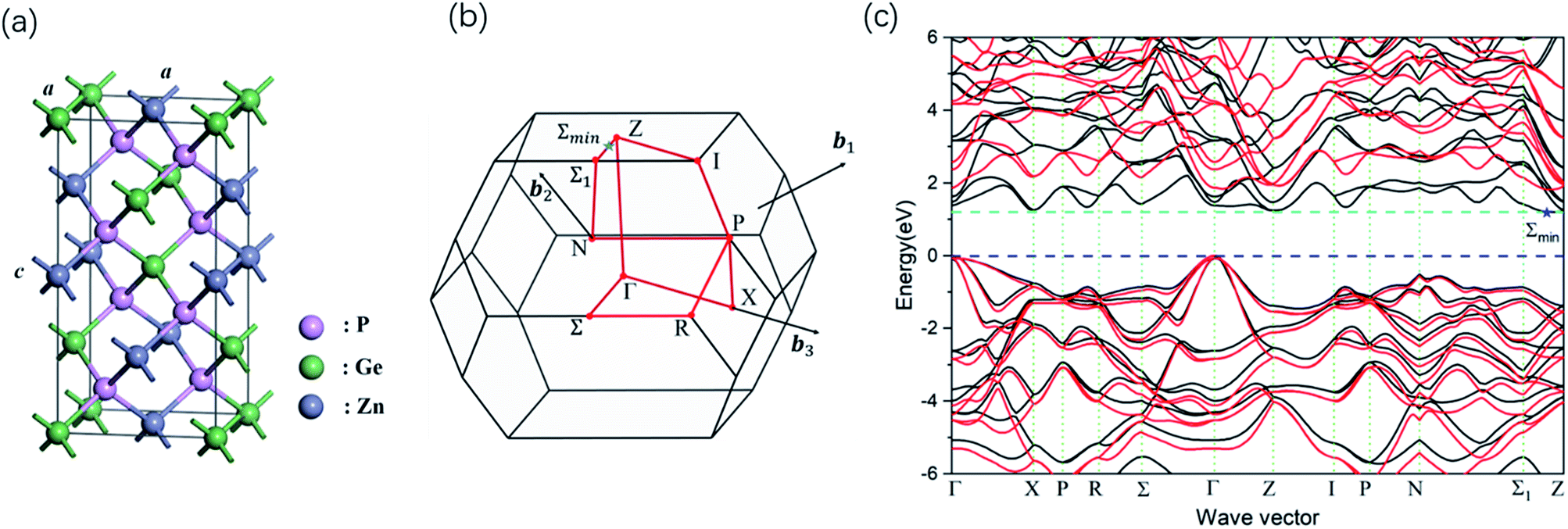 | ||
| Fig. 1 (a) The crystal structures of ZnGeP2 unit cell. The Zn, Ge and P are purple, green and gray balls, respectively. The c-axis is along the z direction. (b) First Brillouin zone (BZ) corresponding to the primitive unit cell of the body centered tetragonal phase ZnGeP2. The red circles representative special k-vector point with highest symmetry in reciprocal space. The red lines indicate segments of the band path, which is Γ-X-P-R-Σ-Γ-Z-I-P-N-Σ1-Z. (c) Band structure of ZnGeP2 calculated with the PBE functional (black lines) and with GW0 (red lines). The zero of the energy is set to the energy of the valence band maximum. | ||
B. Band-structure calculation
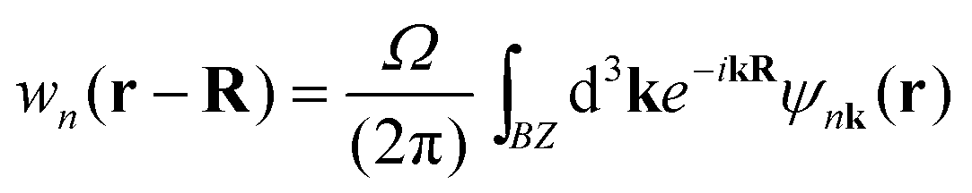
The self-consistent electronic band structures were then have been calculated with PBE, PBEsol, SCAN, mBJ and HSE06 functionals. In these self-consistent calculations, a denser k-pointer sampling of 12 × 12 × 12 was used. The band structure is plotted along the high-symmetry directions in the first Brillouin zone (Fig. 1b). The HSE06 band structure is interpolated using the Maximally-Localized Wannier functions.21 In unit cell R, the Wannier function wn(r) with band n is defined as:
 | (1) |
Quasiparticle energies are calculated as correction to the Kohn–Sham eigenvalues using the GW approximation, following the approach of Rolfling and Louie.22 We first obtain the electronic ground state using density functional theory within the PBE. Then, the quasiparticle excitation spectrum of electrons and holes are calculated with one-body Green's function based on the GW approximation to the electron self-energy.23 The electron–ion interaction is described with pseudopotentials optimized for GW calculations. The exchange and correlation effects among the electrons are described by the electron self-energy operator Σ(E). Assuming that the DFT and quasiparticle wave functions are the same, the quasiparticle energies are iteratively updated by transform one-particle Green's function G1 into the corresponding Dyson's equation for the quasiparticles. For the eigenvalue self-consistent GW calculation, we use a cutoff of 300 eV for the plane wave expansion, a 10 × 10 × 6 k-point mesh, and a total of 224 electronic energy bands. Wannier interpolation is employed to obtain the quasiparticle band structure as there has been used in HSE06 band structure interpolation.
C. Linear and nonlinear optical properties
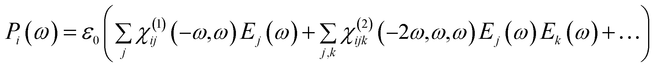
The optical response of a material to the incoming light is to polarize the material. The polarization can be expressing as a Taylor series expansion of the applied electric field strength as following relation:
 | (2) |
 | (3) |
 | (4) |
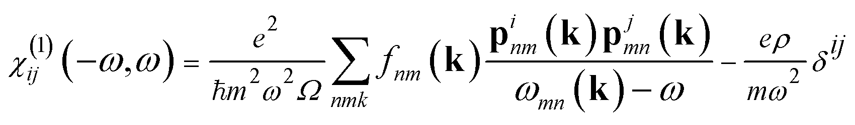
The indices c and v refer to conduction and valence band states respectively. The real part of the dielectric tensor  is obtained by the Kramers–Kronig transformation:
 | (5) |
 | (6) |
The second-order NLO susceptibility tensor χ(2)ijk(−2ω, ω, ω) were calculated within density functional perturbation theory,26 employing the 2n + 1 theorem, as developed by Veithen et al.27 and implemented in the ABINIT software package.28,29 The expression for the second order susceptibility can be generally written as the sum of the three physically different contributions in the form:30
 | (7) |
The three terms describe the contributions of the interband transitions, intra band motion of the electrons and the polarization energy associated with the interband motion to second order susceptibility, respectively. For the linear and nonlinear optical properties calculation, a more fine Brillouin zone was sampled using a Monkhorst–Pack 24 × 24 × 24 grid of special k-point, wave functions were expand in plan-waves up to a kinetic energy cutoff of 20 Hartee, and the number of band is set as 118 to include more empty band. These parameters were found to be necessary for convergence of the nonlinear susceptibilities.
D. Bethe–Salpeter equation
With the Kohn–Sham wave function and quasiparticle energies, we then account for the electron–hole attraction and local-field effects in the linear optical spectra by solving the Bethe–Salpeter equation (BSE) of the two-particle Green's function:31
 | (8) |
We use the implementation of Michael et al.22 and obtain the imaginary part of the dielectric function, ε′′(ω), numerically in a finite frequency interval:
 | (9) |
 is the single-particle velocity operator. The real part is derived by means of the Kramers–Kronig relation from the imaginary part, which is extended with an analytic high frequency tail for this purpose as described by Adolph et al. All electronic states within a distance of 15 eV from the Fermi energy are included.
Results and discussion
A. Structure optimization
ZnGeP2 exhibits the chalcopyrite crystal structure, derived from the III–V zinc blende compounds (GaP) by ordered substitution of group IIB (Zn) and group IVB (Ge) atoms on the group III (Ga) site (Fig. 1a). The introduction of two dissimilar atomic bond lengths (Zn–P and Ge–P) leads to a tetragonal distortion of the cubic zinc blende structure, which is the origin of the birefringence and anisotropic optical properties. Particularly, replacing with dissimilar atomic causes the breaking of inversion symmetry and results in the noncentrosymmetric point group D2d (I2d), which leads to highly anisotropic electronic band structure and nonlinear SHG susceptibility. The body centered tetragonal phase ZnGeP2 unit cell has two independent lattice parameters a and c, the three crystal axes are perpendicular.
We optimized the ZnGeP2 structure using the GGA functionals PBE and PBEsol as well as the SCAN meta-GGA functional. In Table 1 we compared the results with the experiment (lattice constants a = 0.5465 nm, c = 1.0766 nm at room temperature).16,32 The PBE results overestimated the lattice constant, and the SCAN meta-GGA results has the closest match with the experiment. The experiments were performed under room temperature and atmospheric pressure, while our calculations correspond to 0 K and do not consider the thermal lattice expansion. The difference between the structure optimized with SCAN meta-GGA functional and experimental result is therefore negligible. In the following calculations, we used the optimized crystal structure obtained with the SCAN meta-GGA functional.
B. Electronic band structure
The valence band maximums, conduction band minimums and band gaps of ZnGeP2 calculated using different DFT techniques and the GW0 approximation are listed in Table 2, together with the available experimental data.33 The band gap values calculated using PBE and PBEsol (1.191 and 1.227 eV respectively) are consistent with the earlier theoretical studies34 and underestimate the experimental value (2.0 eV). This is a well-known drawback of DFT calculations with local or semilocal exchange–correlation functionals. In order to obtain the improved band gap values, GGA + U (Hubbard term U) approach and scissors shift are often used.35 However, these methods introduce artificial parameters and it is difficult to choose the values of Hubbard term U that are consistent with the experimental results. And the high-level theory go beyond the Kohn–Sham density functional theory hybrid functional and GW approximation obtain correct band gap with little change in band structure, only the energy gap is significantly modified. The results of the calculated band structure with aforementioned methods are shown in the ESI Fig. S1.†The GW0 gives a more reliable band structure due to the inclusion of many-body effect,36 which reduces the localization error. The band gap calculated using GW0 approximation is 1.812 eV, nicely agreed with the experimental values. The hybrid functionals such as HSE06, by introducing a fraction of Fock exchange into the exchange and correlation functionals, can also obtain an improved band gap value. The HSE06 with a 25% exact exchange functional, for instance, gives a 1.883 eV band gap. These two methods are, however, very expensive for larger systems.
The Meta-GGA functionals include the encoded information of shell structures by including the kinetic energy densities. They differentiate the orbital-overlap regions and thus deliver simultaneous accurate ground-state properties.38 We herein used two different types of Meta GGAs, SCAN meta-GGA20 and mBJ,39 to calculate the band structure. The calculated band gap with SCAN is 1.387 eV, which is better than the results of PBE. The semilocal exchange potential mBJ gives a band gap value of 1.896 eV, which is much closer to the experimental value with respect to the usual GGA functionals. Our values are in good agreement with other theoretical reports.37 The mBJ results are comparable in accuracy with the expensive hybrid and GW methods, with the computing cost as low as the GGA calculations.39 The mBJ have been wildly used in other system, for example in thermoelectric material ZnGeSb2.40 Therefore, it can be applied to very large systems in an efficient way.39
The calculated band structure using GW0 approximation is presented in Fig. 1c. The band structure is plotted along the high-symmetry directions in the first Brillouin zone (Fig. 1b). The lowest conduction-band state is located in the point Σmin between the point Z and Σ1. The lowest direct gap is larger than the indirect gap by only a few tens of millielectron volts in the GW0 result. ZnGeP2 is found to have an quasi-direct-gap, in agreement with previous theoretical works.41
Due to the accuracy of GW results, in the following, we discussed primarily the calculated dielectric spectrum using GW approximation and the second order susceptibility calculated using PBE with the scissor shift adjusted according to the GW band gap value.
C. Linear and nonlinear optical properties
For the body centered tetragonal phase ZnGeP2 crystal, there are two independent components of the dielectric tensor, namely ε⊥(=εxx = εyy) and ε‖(=εzz), where the direction z is parallel to the c-axis of the crystal unit cell. These two components can be measured experimentally in ordinary (ε⊥) and extraordinary (ε‖) polarization. The imaginary part of the two components of the linear frequency dependent dielectric, calculated with GW0, are presented in Fig. 2a. The overall shapes of these two components are similar, with differences in the fine structure due to the different directional components of the transition dipole moment at critical points within the materials.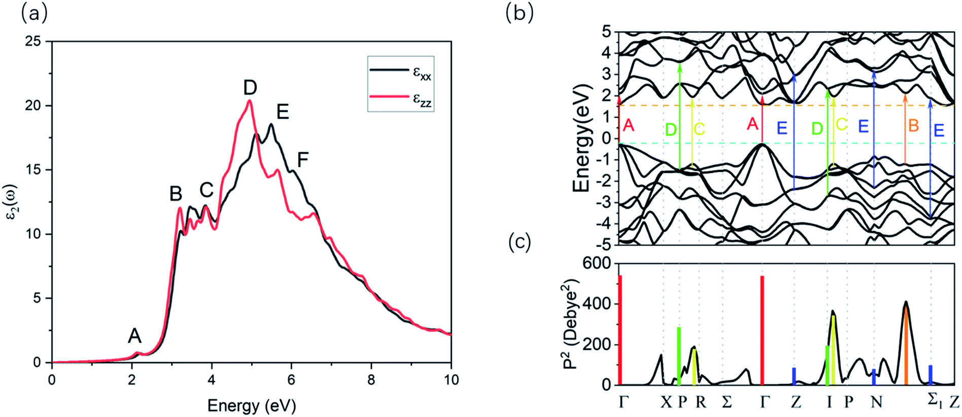 | ||
| Fig. 2 (a) Imaginary part of the xx and zz component of the linear dielectric tensor. (b) The quasiparticle band structure of the ZnGeP2. (c) The matrix elements of the optical transitions. The results calculated with GW0. | ||
The first few optical transitions can be connected with spectral features in the imaginary dielectric functions. The imaginary part of dielectric function ε2(ω) has major peaks at 3.2073 eV (B), 4.94 eV (D) and 5.467 eV (E) and minor peaks at 2.13 eV (A), 3.85 eV (C) and 6.01 eV (F) (Fig. 2a). By analyzing the magnitude of the transition dipole moment (details provided in the ESI Fig. S2†) between the different valence bands of the band edge and the conduction band, the optical transitions related to these peaks can be identified from the band structure (Fig. 2b).
The strength of transitions is revealed by the mod square of the transition dipole vectors P2.42 For all the transitions noted in Fig. 2b, their P2 are shown as vertical colored bars in Fig. 2c. For the transitions with the degenerate initial and final states, the total transition dipole moment summed from all possible transitions is used. The details of all transition dipole moment for the peaks in the imaginary part of dielectric function are provided in Table S1.†
At a number of k points with high symmetry, P2 for transitions between the topmost valence and the lowest conduction band are presented in Fig. 2c as well. The value of P2 is zero for transition between the conduction band minimum (CBM) and valence band maximum (VBM) at the Γ point, implying a forbidden transition. The largest P2 is observed between the N and Σ1, which result in the peak B. And the second and third largest P2 locate around P k-point, result in the peak C. The peaks A, D and E relate to transition between the lower valence and the higher conduction band. The peak A is mainly caused by the high transition dipole moment of Γ point, but its intensity is weak due to the low density of states. The spectral features are therefore sensitive to the factors including the band gap, the state degeneracy as well as the energy of certain k points, which can all be influenced by the quasiparticle effects.
The second-order nonlinear polarization P(2ω) at frequency 2ω is determined by a third-rank electric susceptibility tensor χ(2):Pi(2ω) = χ(2)ijk (−2ω, ω, ω)Ej(ω)Ek(ω), which correlates with the emitting SHG field. We used the PBE functional to generate the wave functions for the nonlinear susceptibility evaluation, and a scissors shift tuned to the GW value is applied to widen the band gap. Fig. 3 shows the nonvanishing independent components of the SHG susceptibility tensors. ZnGeP2 belong to the D2d (I2m) point group with effectively only two independent nontrivial SHG susceptibility tensor element that satisfies χ(2)zxy = χ(2)zyx and χ(2)xyz = χ(2)xzy = χ(2)yxz = χ(2)yzx. In the energy range of 0–1.3 eV, the two SHG susceptibility tensors elements xyz and zxy present no difference χ(2)zxy = χ(2)xyz, due to the negligible dispersion in the refractive index (Kleinman symmetry condition).
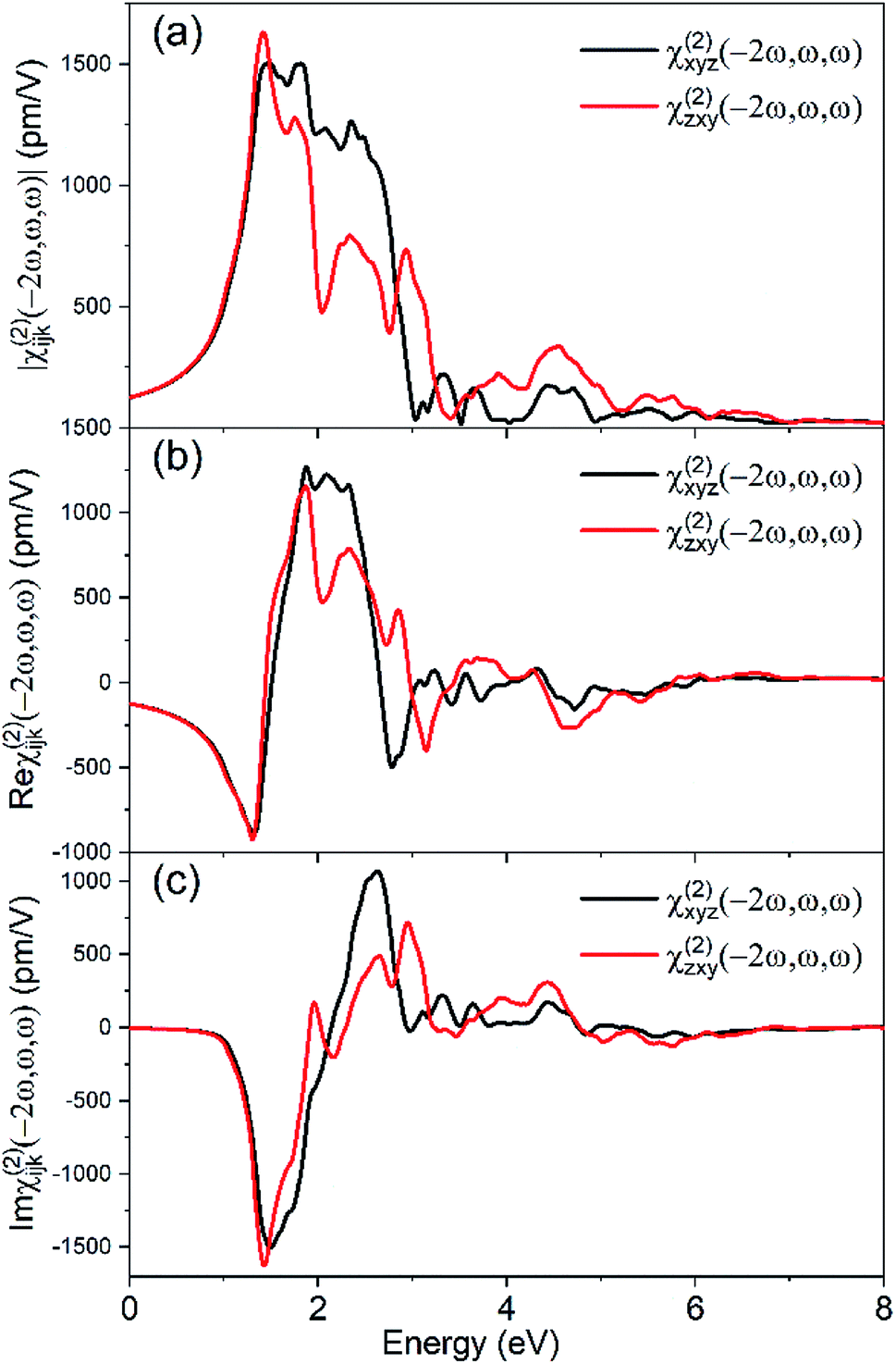 | ||
| Fig. 3 The calculated frequency response of the SHG susceptibilities in ZnGeP2 with (a) magnitude, (b) real and (c) imaginary component. Calculations were done at the level of the GGA and have been scissors-corrected. | ||
In the following, we compared the results of PBE and GW0 to discuss the quasi-particle effects, and the results of BSE and GW0 for the excitonic effects.
D. Quasi-particle effects
Compared to PBE, the GW0 quasiparticle shifts the band gap by 0.621 eV and the band shows higher dispersion (Fig. 2a). This is consistent with the fact that the quasiparticle effects lead to stronger interactions of electrons. This change of band gap causes the spectra to significantly blue-shift.The quasiparticle effects also lead to a plethora of minor differences in the conductor band structure. Some of them (A, B, C, X) are noted in Fig. 4, with higher difference energy between conductor band minimum (CBM) for GW0 calculation. These local perturbations are related to the fine variations in the spectral features. For instance, Γc1 point energy is closer to the conductor band minimum (CBM), while the energy differences between the Γc1, Γc2 and Γc3 increase. The calculated energy difference between Γc2 and CBM (ΔECBM) of GW0 is 1.183 eV, while that of PBE is 0.273 eV, which generates a blue shift for the peak A. We further calculated the real and imaginary components of the dielectric function at GGA and GW0 level; the response curves are provided in Fig. 5. The use of quasiparticle energy is necessary, due to the problem of bandgap underestimation in DFT and the consequent overestimation of the real part of the dielectric function.27
 | ||
| Fig. 4 The band structure of ZnGeP2 calculated with (a) PBE, and (b) GW0. | ||
 | ||
| Fig. 5 Calculated dielectric functions for ZnGeP2 with PBE and GW0. (a) Real ordinary components. (b) Real extraordinary components. (c) Imaginary ordinary components. (d) Imaginary extraordinary components. The dielectric functions for the electric field polarization along x-direction (E‖a-axis) (a, c) and z-direction (E‖c-axis) (b, d) are calculated with PBE and GW0. Only direct interband optical transitions are considered in the calculation. | ||
For the second order susceptibility, The calculated χ(2)zxy using the GW benchmarked band gap value is ∼136.8 pm V−1 at 0.115 eV (10.6 μm), and ∼138 pm V−1 at 0.13 eV (9.6 μm), which is in better agreement with experiment comparing the results of standard PBE calculation (Fig. 6), which demonstrates the importance of band gap value corrections via a scissors shift. Furthermore, the nonlinear susceptibility calculated with the scissors shift is significantly reduced, and the peak patterns also have non-negligible changes. The use of scissors corrections is necessary due to the problem of bandgap underestimation in DFT and the consequent overestimation of the nonlinear susceptibility. These significant variations generated by the adjustment of band gap value suggest the importance of the underlying quasiparticle effects.
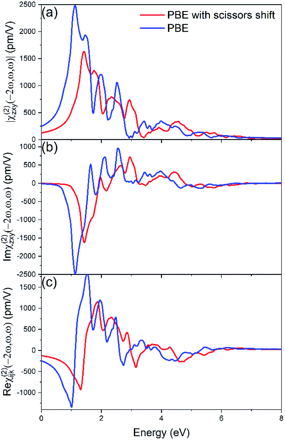 | ||
| Fig. 6 SHG zxy components of the nonlinear susceptibility for ZnGeP2 calculated with PBE without (blue lines) and with a scissors shift (red lines). (a) Magnitude, (b) imaginary and (c) real components. | ||
E. Exciton effects
The energy difference of the first peak in the imaginary part of the GW0 and BSE spectra gives a fairly large exciton binding energy of ∼130 meV, which indicates a non-negligible excitonic effect. By comparing the calculated dielectric spectra of BSE and GW0 (Fig. 7), we found that exciton effects significantly enhance the peak intensity in the long wave regime of the dielectric spectrum and reduce the linewidth of signal. The enhancement of the peak between 3.0–4.0 eV is due to the excitonic resonances absorption. The electron–hole pairs in this energy regime exist in the bound states (excitons), which create the resonant absorption and enhance the peak intensity. A red shift of signal is also observed in the BSE result, since the Coulomb potential of the exciton can reduce the system total energy. | ||
| Fig. 7 Imaginary part ε2(ω) of the linear dielectric function of ZnGeP2 in the ordinary polarization. The experimental data in the energy range 1.5–6.0 eV are taken from ref. 43. | ||
More interestingly, a small absorption peak appears near the band edge for energy around 2.2 eV in the BSE absorption spectrum. This is due to the known effect of excitons to enhance the band edge absorption. The peak is absent in the experimental result due to the lack of sensitivity of rotating-analyzer ellipsometry to small ε2, all ε2 values, which were below the absorption edges near 2.3 eV and neglected.43 The real and extraordinary components dielectric functions are provided in Fig. S3† and absorption intensity are provided in Fig. S4.† The study provides first principles guidance in the selection and design of novel crystals for mid-IR NLO applications.44
Conclusions
In this study, we compared the structural, electronic and optical properties of ZnGeP2 crystal calculated with various ab initio methods in order to address the influences of quasiparticle and excitonic effects on its optical absorption.By comparing the DFT band structure of ZnGeP2 with the results from the GW0 calculation, we find that the self-energy correction essentially widens the band gap, and leads to the valence band with higher dispersion. The quasiparticle effects also change the electronic state energy and degeneracy at some high symmetry point in the conduction band.
By solving the Bethe–Salpeter equation to include the effects of the electron–hole interaction, we obtain the dielectric spectra in good quantitative agreement with experiments. Based on the peak positions in the imaginary part of the dielectric function obtained from the BSE and the independent-quasiparticle approximation, we deduce an exciton binding energy 0.13 eV for ZnGeP2 crystal.
The band structure and optical spectra calculated with mBJ is also good in agreement with the experimental results, and is better than other methods besides BSE. When the excitonic effects can be ignore, mBJ could be a better method for larger system.
Conflicts of interest
There are no conflicts to declare.Acknowledgements
The work is supported by National Natural Science Foundation of China under grant numbers 51672003 and 51872279.References
- M. Schellhorn, G. Spindler and M. Eichhorn, Opt. Express, 2018, 26, 1402–1410 CrossRef CAS PubMed.
- P. A. Budni, L. A. Pomeranz, M. L. Lemons, C. A. Miller, J. R. Mosto and E. P. Chicklis, J. Opt. Soc. Am. B, 2000, 17, 723–728 CrossRef CAS.
- M. Henriksson, M. Tiihonen, V. Pasiskevicius and F. Laurell, Opt. Lett., 2006, 31, 1878–1880 CrossRef CAS.
- A. A. Ionin, I. O. Kinyaevskiy, Y. M. Klimachev, Y. V. Kochetkov, A. Y. Kozlov, L. V. Seleznev, D. V. Sinitsyn, D. S. Zemtsov and Y. M. Andreev, Laser Phys., 2018, 28, 025401 CrossRef.
- A. I. Gribenyukov, S. M. Vatnik, V. V. Demin, S. N. Podzyvalov, I. G. Polovtsev and N. N. Yudin, Quantum Electron., 2018, 48, 603–606 CrossRef CAS.
- D. Creeden, P. A. Ketteridge, P. A. Budni, S. D. Setzler, Y. E. Young, J. C. McCarthy, K. Zawilski, P. G. Schunemann, T. M. Pollak, E. P. Chicklis and M. Jiang, Opt. Lett., 2008, 33, 315–317 CrossRef CAS.
- A. Hemming, J. Richards, A. Davidson, N. Carmody, S. Bennetts, N. Simakov and J. Haub, Opt. Express, 2013, 21, 10062–10069 CrossRef CAS.
- N. C. Giles, L. Bai, M. M. Chirila, N. Y. Garces, K. T. Stevens, P. G. Schunemann, S. D. Setzler and T. M. Pollak, J. Appl. Phys., 2003, 93, 8975–8981 CrossRef CAS.
- N. Dietz, I. Tsveybak, W. Ruderman, G. Wood and K. J. Bachmann, Appl. Phys. Lett., 1994, 65, 2759–2761 CrossRef CAS.
- D.-H. Yang, B.-J. Zhao, B.-J. Chen, S.-F. Zhu, Z.-Y. He, Z.-R. Zhao and M.-D. Liu, Mater. Res. Express, 2017, 4, 075906 CrossRef.
- D. Swain, R. Singh, V. K. Singh, N. V. Krishna, L. Giribabu and S. V. Rao, J. Mater. Chem. C, 2014, 2, 1711–1722 RSC.
- P. G. Schunemann, K. T. Zawilski, L. A. Pomeranz, D. J. Creeden and P. A. Budni, J. Opt. Soc. Am. B, 2016, 33, D36–D43 CrossRef CAS.
- X. Jiang, M. S. Miao and W. R. L. Lambrecht, Phys. Rev. B: Condens. Matter Mater. Phys., 2005, 71, 205212 CrossRef.
- X. Jiang, M. S. Miao and W. R. L. Lambrecht, Phys. Rev. B: Condens. Matter Mater. Phys., 2006, 73, 193203 CrossRef.
- K. V. Shportko, Vib. Spectrosc., 2015, 80, 1–5 CrossRef CAS.
- A. Continenza, S. Massidda, A. J. Freeman, T. M. Depascale, F. Meloni and M. Serra, Phys. Rev. B: Condens. Matter Mater. Phys., 1992, 46, 10070–10077 CrossRef CAS.
- M. Gajdos, K. Hummer, G. Kresse, J. Furthmuller and F. Bechstedt, Phys. Rev. B: Condens. Matter Mater. Phys., 2006, 73, 045112 CrossRef.
- G. Kresse and J. Furthmuller, Phys. Rev. B: Condens. Matter Mater. Phys., 1996, 54, 11169–11186 CrossRef CAS.
- J. P. Perdew, A. Ruzsinszky, G. I. Csonka, O. A. Vydrov, G. E. Scuseria, L. A. Constantin, X. Zhou and K. Burke, Phys. Rev. Lett., 2008, 100, 136406 CrossRef.
- J. Sun, A. Ruzsinszky and J. P. Perdew, Phys. Rev. Lett., 2015, 115, 036402 CrossRef.
- A. A. Mostofi, J. R. Yates, Y.-S. Lee, I. Souza, D. Vanderbilt and N. Marzari, Comput. Phys. Commun., 2008, 178, 685–699 CrossRef CAS.
- M. Rohlfing and S. G. Louie, Phys. Rev. B: Condens. Matter Mater. Phys., 2000, 62, 4927–4944 CrossRef CAS.
- L. Yang, M. L. Cohen and S. G. Louie, Nano Lett., 2007, 7, 3112–3115 CrossRef CAS.
- J. E. Sipe and E. Ghahramani, Phys. Rev. B: Condens. Matter Mater. Phys., 1993, 48, 11705–11722 CrossRef CAS.
- B. Adolph, J. Furthmüller and F. Bechstedt, Phys. Rev. B: Condens. Matter Mater. Phys., 2001, 63, 125108 CrossRef.
- S. Baroni, S. de Gironcoli, A. Dal Corso and P. Giannozzi, Rev. Mod. Phys., 2001, 73, 515–562 CrossRef CAS.
- M. Veithen, X. Gonze and P. Ghosez, Phys. Rev. B: Condens. Matter Mater. Phys., 2005, 71, 125107 CrossRef.
- X. Gonze, B. Amadon, P. M. Anglade, J. M. Beuken, F. Bottin, P. Boulanger, F. Bruneval, D. Caliste, R. Caracas, M. Cote, T. Deutsch, L. Genovese, P. Ghosez, M. Giantomassi, S. Goedecker, D. R. Hamann, P. Hermet, F. Jollet, G. Jomard, S. Leroux, M. Mancini, S. Mazevet, M. J. T. Oliveira, G. Onida, Y. Pouillon, T. Rangel, G. M. Rignanese, D. Sangalli, R. Shaltaf, M. Torrent, M. J. Verstraete, G. Zerah and J. W. Zwanziger, Comput. Phys. Commun., 2009, 180, 2582–2615 CrossRef CAS.
- X. Gonze, F. Jollet, F. A. Araujo, D. Adams, B. Amadon, T. Applencourt, C. Audouze, J. M. Beuken, J. Bieder, A. Bokhanchuk, E. Bousquet, F. Bruneval, D. Caliste, M. Cote, F. Dahm, F. Da Pieve, M. Delaveau, M. Di Gennaro, B. Dorado, C. Espejo, G. Geneste, L. Genovese, A. Gerossier, M. Giantomassi, Y. Gillet, D. R. Hamann, L. He, G. Jomard, J. L. Janssen, S. Le Roux, A. Levitt, A. Lherbier, F. Liu, I. Lukacevic, A. Martin, C. Martins, M. J. T. Oliveira, S. Ponce, Y. Pouillon, T. Rangel, G. M. Rignanese, A. H. Romero, B. Rousseau, O. Rubel, A. A. Shukri, M. Stankovski, M. Torrent, M. J. Van Setten, B. Van Troeye, M. J. Verstraete, D. Waroquiers, J. Wiktor, B. Xu, A. Zhou and J. W. Zwanziger, Comput. Phys. Commun., 2016, 205, 106–131 CrossRef CAS.
- J. L. P. Hughes and J. E. Sipe, Phys. Rev. B: Condens. Matter Mater. Phys., 1996, 53, 10751–10763 CrossRef CAS.
- G. Onida, L. Reining and A. Rubio, Rev. Mod. Phys., 2002, 74, 601–659 CrossRef CAS.
- M. D. Lind and R. W. Grant, J. Chem. Phys., 1973, 58, 357–362 CrossRef CAS.
- D. M. Hofmann, N. G. Romanov, W. Gehlhoff, D. Pfisterer, B. K. Meyer, D. Azamat and A. Hoffmann, Phys. B, 2003, 340–342, 978–981 CrossRef CAS.
- S. Limpijumnong, W. R. L. Lambrecht and B. Segall, Phys. Rev. B: Condens. Matter Mater. Phys., 1999, 60, 8087–8096 CrossRef CAS.
- S. Piccinin, Phys. Chem. Chem. Phys., 2019, 21, 2957–2967 RSC.
- G. Onida, L. Reining and A. Rubio, Rev. Mod. Phys., 2002, 74, 601–659 CrossRef CAS.
- P. C. Sreeparvathy, V. Kanchana and G. Vaitheeswaran, J. Appl. Phys., 2016, 119, 8 CrossRef.
- J. Sun, B. Xiao and A. Ruzsinszky, J. Chem. Phys., 2012, 137, 051101 CrossRef.
- F. Tran and P. Blaha, Phys. Rev. Lett., 2009, 102, 226401 CrossRef.
- P. C. Sreeparvathy, V. Kanchana, G. Vaitheeswaran and N. E. Christensen, Phys. Chem. Chem. Phys., 2016, 18, 26275–26283 RSC.
- V. L. Shaposhnikov, A. V. Krivosheeva, V. E. Borisenko, J. L. Lazzari and F. A. d'Avitaya, Phys. Rev. B: Condens. Matter Mater. Phys., 2012, 85, 205201 CrossRef.
- W. Meng, X. Wang, Z. Xiao, J. Wang, D. B. Mitzi and Y. Yan, J. Phys. Chem. Lett., 2017, 8, 2999–3007 CrossRef CAS.
- V. Blickle, K. Flock, N. Dietz and D. E. Aspnes, Appl. Phys. Lett., 2002, 81, 628–630 CrossRef CAS.
- L. Kang, D. M. Ramo, Z. S. Lin, P. D. Bristowe, J. G. Qin and C. T. Chen, J. Mater. Chem. C, 2013, 1, 7363–7370 RSC.
Footnote |
| † Electronic supplementary information (ESI) available. See DOI: 10.1039/c9ra08172k |
| This journal is © The Royal Society of Chemistry 2019 |