
 Open Access Article
 This Open Access Article is licensed under a Creative Commons Attribution-Non Commercial 3.0 Unported Licence
Cation exchange synthesis of CuInxGa1−xSe2 nanowires and their implementation in photovoltaic devices†
Guanwei Jia‡a,
Kun Wang‡
b,
Baokun Liub,
Peixu Yangb,
Jinhui Liub,
Weidong Zhangb,
Rongbin Lic,
Chengduo Wangb,
Shaojun Zhangb and
Jiang Du *bd
*bd
aSchool of Physics and Electronics, Henan University, Kaifeng 475004, China
bHenan Province Industrial Technology Research Institute of Resources and Materials, Zhengzhou University, Zhengzhou 450001, China. E-mail: 0210927@163.com
cSchool of Metallurgical and Ecological Engineering, University of Science and Technology Beijing, Beijing 100083, China
dDepartment of Chemical Engineering, Texas Materials Institute, Center for Nano- and Molecular Science and Technology, The University of Texas at Austin, Austin, TX 78712, USA
First published on 4th November 2019
Abstract
CuInxGa1−xSe2 (CIGS) nanowires were synthesized for the first time through an in situ cation exchange reaction by using CuInSe2 (CIS) nanowires as a template material and Ga-OLA complexes as the Ga source. These CIGS nanowires maintain nearly the same morphology as CIS nanowires, and the Ga/In ratio can be controlled through adjusting the concentration of Ga-OLA complexes. The characteristics of adjustable band gap and highly effective light-absorbances have been achieved for these CIGS nanowires. The light-absorbing layer in photovoltaic devices (PVs) can be assembled by employing CIGS nanowires as a solar-energy material for enhancing the photovoltaic response. The highest power conversion efficiency of solar thin film semiconductors is more than 20%, achieved by the Cu(InxGa1−x)Se2 (CIGS) thin-film solar cells. Therefore, these CIGS nanowires have a great potential to be utilized as light absorber materials for high efficiency single nanowire solar cells and to generate bulk heterojunction devices.
1. Introduction
Copper indium gallium selenide (CuInxGa1−xSe2, CIGS) and related I-III-VI2 compounds are applied widely as light-absorbing materials in thin-film solar cells.1–4 In virtue of their high absorption coefficients, optimal band-gaps, and good photostability, these compounds show excellent photovoltaic properties.5–7 CIGS nanowires are employed as polycrystalline films for high efficiency. CIGS-based devices can achieve as much as 20% power conversion efficiency (PCE).8 Vacuum procedures and their related equipment are demanded for traditional manufacturing of CIGS-based devices, which leads to an increase in the manufacturing costs and block their scale up.9 One of the significant cutting cost approaches for the preparation of CIGS-based devices is colloidal nanocrystal ink deposition on the inorganic light-absorber layer, which has been reported by a number of research teams,5,10–13 although their reported PCE values were too low for commercial promotion.The main shortcoming of thin-film PVs with colloidal nanocrystal absorbing layers is the large number of grain boundaries and interfaces in the film, which hinder carrier diffusion and reduce PV efficiency.13,14 Furthermore, the electrically insulating organic capping ligands applied to fix the nanocrystals to the device have a strong influence on the PVs efficiency. In order to solve these problems, thin film PVs are pre-annealed and sintered into polycrystalline films at 500 °C in a Se gas environment.11,15 H the selenization process still needs high temperatures and leads to a hard control of the stoichiometry. Compared with nanocrystals, nanowires eliminate the grain boundaries along the radial direction and also are facile to scatter in solvents.16 Therefore, the advantage of nanowire application is in the improvement of the minority carrier diffusion range of motion and in a higher efficiency of sprayed inorganic PVs, without the need for sintering.17–19
Crystallized CuInSe2 (CIS) nanowires have been fabricated through vapor–liquid–solid (VLS)20 or solution–liquid–solid (SLS)16 techniques. Photovoltaic solar cells need high band gaps to improve their efficiency,21 but the band gap of synthesized CIS nanowires is as low as ∼1 eV.16 Ga has been added to CIS to form CIGS, which can increase the band gap,21 and improve the open circuit voltage and efficiency.22 Therefore, the use of Ga to synthesize crystallized CIGS nanowires is desired.
According to our research, it is difficult to synthesize CIGS via the SLS method within one step (TOP as the solvent and Bi as the seed). Ga is hard to be combined with Cu, In and Se atoms during this SLS growth process.
Several methods for the direct synthesis of these nanocrystals with desired compositions and morphology have been proved to be difficult. A new method based on cation exchange reactions has attracted interest and demonstrated advantages in the direct synthesis of nanocrystals.23–26 The thermodynamic driving force for this ion exchange is a balance between the solvation energy of the ions and the lattice binding energy before and after exchange.24,27–29 Thus, the solvation energies of the ions must be similar to permit facile exchange.25 The formation mechanism of CIGS nanoparticles synthesized by using heating-up processes has been well illustrated.30 CIGS nanoparticles were assembled utilizing the thermal decomposition of Cu, In, Ga and selenium-oleylamine (OLA) complexes by means of the heating-up procedure. The phase transition sequence was CuSe → CIS → CIGS.30 Based on this formation mechanism of CIGS nanoparticles, we successfully synthesized CIGS nanowires through an in situ cation exchange reaction by using CIS nanowires as the template material and Ga-OLA complexes as the Ga source. As the reaction temperature was increased over 230 °C, the concentration of monomers containing Ga ions resulting from the thermal decomposition of the OLA-Ga complexes increased slowly and exchanged the In atoms30 to form CIGS shells on the surface of CIS nanowires. Then, the CIS nanowires reacted with the inward-diffused Ga ions to form the CIGS phase. CIGS nanowires maintain nearly the same morphology as CIS nanowires, and the Ga/In ratio can be tuned by varying the concentration of the Ga-OLA complexes. This in situ cation exchange reaction might be generally used for converting CIS to CIGS.
2. Materials and methods
2.1 Chemicals
All chemicals were used as received. Tetrahydrofuran (THF, anhydrous, 99.9%, inhibitor-free), sodium bis(trimethylsilyl)-amide (Na[N(SiMe3)2], 1.0 M in THF), bismuth chloride (BiCl3, 98%), diphenyl ether (DPE, 99%), copper (I) acetate (97%), indium (III) acetate (99.99%), gallium (III) chloride (GaCl3; 99.9999%), elemental selenium (Se, 99.99%), trioctylphosphine (TOP, 90%), and oleic acid (OA, 99%) were obtained from Aldrich; methanol (MeOH), toluene, and hexane were purchased from Fisher Scientific. A polyvinylpyrrolidone-hexadecane (PVP-HDE) copolymer (Ganex V 216, MW = 7300 g mol−1, product ID 72289D) was purchased from ISP Technologies, Inc.2.2 Bismuth nanocrystal synthesis
Tris[bis(trimethylsilyl)amino] bismuth (Bi[N(SiMe3)2]3) was synthesized by previously reported methods and dissolved in THF to obtain a 1 M solution. 5.0 g of Ganex V216 and 15 g of diphenyl ether were combined in a 100 mL three-neck flask. The flask was attached to a Schlenk line, placed under vacuum, heated to 70 °C, and allowed to degas for 1.5 h while stirring. Simultaneously, 0.5 mL of Bi[N(SiMe3)2]3/THF was mixed with 2.0 mL of 1 M NaN-(SiMe3)2 in THF and placed into a syringe. After the Ganex V216 and diphenyl ether solution was degassed, the flask was refilled with N2 and the temperature was increased to 180 °C. At 180 °C, the Bi precursor solution was quickly injected into the hot solution and reacted for 30 min. After 30 min, the mixture was cooled to 60 °C and 15 mL of room-temperature toluene was added. Bi nanocrystals were isolated by centrifuging the reaction product for 3 min at 5000 rpm. The supernatant was collected, and the precipitate was discarded. Thirty milliliters of MeOH was added to the supernatant and centrifuged for 5 min at 10![[thin space (1/6-em)]](https://www.rsc.org/images/entities/char_2009.gif) 000 rpm. The supernatant was discarded. The precipitate was dispersed in 10 mL of toluene. This process was repeated several times and the final precipitate was dispersed and stored in toluene at a concentration of 5 mg mL−1. The Bi nanocrystals were spherical with an average diameter of 12 nm (Fig. S1, ESI†).
000 rpm. The supernatant was discarded. The precipitate was dispersed in 10 mL of toluene. This process was repeated several times and the final precipitate was dispersed and stored in toluene at a concentration of 5 mg mL−1. The Bi nanocrystals were spherical with an average diameter of 12 nm (Fig. S1, ESI†).
2.3 CuInSe2 nanowire synthesis
A 1 M stock solution of Se in TOP (TOP/Se) was made by dissolving 1.58 g of Se powder in 20 mL of TOP. This solution was made in a glovebox under inert atmosphere, stirred overnight to ensure that Se was completely dissolved, and stored in the same glovebox. Copper acetate (30.6 mg, 0.25 mmol), indium acetate (70.3 mg, 0.25 mmol), 0.25 mL of OA, and 4 mL of TOP were combined in a 25 mL three-neck flask. The flask was attached to a Schlenk line and degassed while heating to 100 °C. After reaching 100 °C, the solution was held under vacuum for 15 min and stirred vigorously. The flask was then filled with N2 and cooled to room temperature under N2 flow. In a separate 100 mL three-neck flask, 8.5 mL of TOP was added, and the flask was attached to the Schlenk line and degassed under vacuum at room temperature for 5 min. TOP was heated to 360 °C under N2 flow. The Cu and In precursor solution was then combined with 0.5 mL of the 1 M TOP/Se stock solution and placed in a syringe. To initiate the reaction, 0.25 mL of a 5 mg mL−1 solution of Bi nanocrystals in toluene was swiftly injected into hot TOP, followed immediately by the Cu, In, and Se precursor solution. The reaction mixture immediately turned from a light yellow color to dark brown with the formation of some black precipitate. The reaction proceeded for 5 min followed by the removal of the heating mantle, allowing the products to cool to ∼50 °C. Ten milliliters of toluene was then injected into the flask, after which the solution was removed from the Schlenk line. To separate and clean the products, this mixture was centrifuged at 4000 rpm for 5 min. The supernatant was discarded, and the precipitate was redispersed in 30 mL of toluene. This cleaning procedure was repeated three times, and the final product was redispersed in ∼10 mL of toluene. Tens of milligrams of CIS nanowires are typically obtained with this procedure.2.4 CuInxGa1−xSe2 nanowire synthesis
CuInSe2 (CIS) nanowires (0.20 g, 0.6 mmol), GaCl3 (0.42 g, 2.4 mmol) and OLA (20 mL) were added into a 25 mL three-neck flask in a glovebox under N2 atmosphere. The Ga/CuInSe2 mole ratio in the reaction mixture varied from 1:1 to 8:1. The flask was attached to a Schlenk line and degassed while heating to 110 °C. After reaching 110 °C, the solution was held under vacuum for 60 min and stirred vigorously. Then, the solution was heated to 260 °C under N2 flow. After reaching 260 °C, the reaction proceeded for 30 min followed by the removal of the heating mantle, allowing the products to cool to ∼60 °C. The product was purified by precipitation with excess ethanol (antisolvent) followed by centrifugation at 4000 rpm for 3 min. The supernatant was discarded, and the precipitate was redispersed in 30 mL of toluene. This cleaning procedure was repeated three times, and the final product was redispersed in toluene.
2.5 Material characterization
Current–potential (IV) characteristics were collected using a Keithley 2400 source meter under AM1.5G illumination (100 mW cm−2). A NIST calibrated Si photodiode (Hamamatsu, S1787-08) was used to tune the light intensity. External quantum efficiency (EQE) was measured as previously described. Monochromatic light (Newport Cornerstone 260 1/4M) at wavelengths ranging from 300 to 1300 nm in 10 nm increments was chopped at 213 Hz and focused to a 1 mm diameter spot size on the device at zero bias. EQE was measured using a lock-in amplifier (Stanford Research Systems, model SR830) after calibrating light intensity with silicon (Hamamatsu) and germanium (Judson) photodiodes.Low-resolution transmission electron microscopy (TEM) images were acquired on a FEI Tecnai Spirit Bio Twin operated at 80 kV. High-resolution transmission microscopy (HRTEM) images were acquired on a field emission JEOL 2010F TEM operated at 200 kV. The JEOL 2010F TEM was equipped with an Oxford INCA EDS detector, which was used to collect EDS data. UV-vis-NIR absorbance spectra were acquired with a Varian Cary 500 UV-vis-NIR spectrophotometer.
2.6 Device fabrication
CIGS NWs PVs were fabricated with a layered Au/CIGS/CdS/i-ZnO/indium tin oxide (ITO) device structure. The 5 nm thick Cr layer and 60 nm thick Au layer were deposited onto soda-lime glass (Delta Technologies, 25 mm × 25 mm × 1.1 mm polished float glass) in sequence by thermal deposition. The CIGS NW film was obtained by spraying CIGS NWs (dispersed in toluene) on the substrate at room temperature. The substrate was placed on a hot plate at 90 °C, and then, 0.9 mL of the previously made aqueous solution of 1.25 mL of 15 mM CdSO4 (Aldrich, 99.999%), 2.2 mL of 1.5 M thiourea (Fluka, 99%), and 2.8 mL of 18 M NH4OH (Fisher Scientific, Certified ACS) was placed on the substrate. After 2 min, the substrate was rinsed with deionized water and dried in air. ZnO/ITO top contacts were deposited by radio frequency (rf) sputtering from ZnO (99.9%, Lesker) and ITO (99.99% 90:10 In2O3/SnO2, Lesker) precursors. The active region of the device was 8 mm2. Silver paint was applied for electrical contact to the devices.
3. Results
Fig. 1 (a) and (b) show the TEM images of CuInSe2 nanowires fabricated through the Bi nanocrystal-seeded SLS growth mechanism. XRD measurements (Fig. 2a) demonstrated that the nanowires were crystalline, which agreed with tetragonal (chalcopyrite) CIS. The length and the mean diameter of CuInSe2 nanowires are several micrometers and 25 nm, respectively. The CuInSe2 nanowires are straight and have a smooth surface (Fig. 1b). TEM image (Fig. 1c) of CuIn0.61Ga0.39Se2 nanowires obtained by Ga ion exchange reaction illustrates similar shapes to the original CuInSe2 nanowires. HR-TEM image (Fig. 1e) confirms the crystallinity of CuIn0.61Ga0.39Se2 nanowires and XRD (Fig. 2d) shows that the diffraction peaks shift to higher 2θ as the result of larger In atoms being substituted by smaller Ga atoms, resulting in the reduction of lattice spacing. Likewise, a similar formation mechanism of CIGS nanoparticles synthesized in OLA has been elaborated.5,30 The surface of the nanowires becomes a little rougher after the Ga ion exchange reaction (Fig. 1d), which can be attributed to Ga ion exchange and their inward diffusion from the surface of CIS nanowires. There is no significant morphology change in the CuIn0.98Ga0.02Se2 and CuIn0.89Ga0.11Se2 nanowires with a lower Ga content (Fig. S2, ESI†). When the Ga/CuInSe2 mole ratio in the reaction mixture is increased to 8:1, a porous structure is formed in the nanowires and the yield becomes lower (Fig. S3, ESI†).
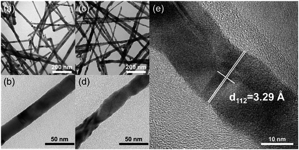 | ||
| Fig. 1 TEM images of (a) and (b) CuInSe2 nanowires; (c) and (d) CuIn0.61Ga0.39Se2 nanowires, and (e) HR-TEM image of (c). | ||
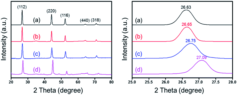 | ||
| Fig. 2 XRD patterns of CIGS nanowires fabricated by adjusting In:Ga ratios: (a) CuInSe2, (b) CuIn0.98Ga0.02Se2, (c) CuIn0.89Ga0.11Se2, (d) CuIn0.61Ga0.39Se2. The indexing of the peaks indicated in (a) matches the desired peak positions for chalcopyrite composites. | ||
As the solvation energy of the Ga ions must be similar to the lattice binding energy before and after exchange, the solvent selection for the Ga ion exchange to CIS nanowires is important. TOP and triethyleneglycol (TEG) were both applied in this reaction as solvents. However, there is no noticeable XRD diffraction shift in peaks or EDS variation. This might be due to the high Ga-TOP and Ga-TEG solvation energies.
Fig. 2 shows XRD patterns of CuInxGa1−xSe2 with x ranging from 0.61 to 1. All patterns are consistent with the chalcopyrite (tetragonal) structure. The Ga/CuInSe2 mole ratio in the reaction mixture is (a) 1:1, (b) 2:1 and (c) 4:1. The diffraction peaks shift from 26.63° to 27.09° because larger In atoms are substituted by smaller Ga atoms, and the lattice spacing is reduced. EDS measurements on different CIGS nanowires illustrate the variation in Cu/In/Ga/Se ratio from nanowire to nanowire. The room temperature absorbance spectra confirmed the band gap energies of CIGS nanowires, as shown in Fig. 3 (CuInSe2, 0.95 eV; CuIn0.61Ga0.39Se2, 1.13 eV); the values for nanowire dispersions were consistent with energies of the corresponding bulk compounds: 0.95 eV and 1.12 eV.21 The absorbance spectra of CuIn0.98Ga0.02Se2 and CuIn0.89Ga0.11Se2 nanowires are similar to that of CuInSe2 due to the low Ga:In ratio (Fig. S4, ESI†).
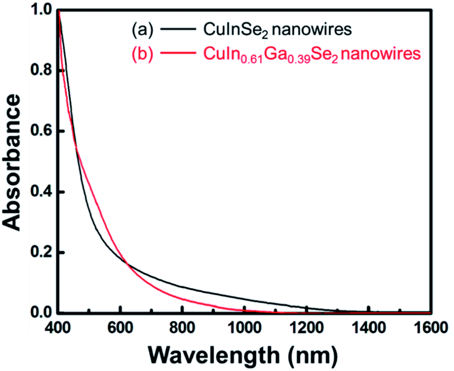 | ||
| Fig. 3 Room temperature absorbance spectra of (a) CuInSe2 nanowires and (b) CuIn0.61Ga0.39Se2 nanowires dispersed in toluene. | ||
The local atomic composition of the nanowires has been examined by energy-dispersive X-ray spectroscopy (EDS). Fig. 4a shows the EDS line scan of CuInSe2. The content of Cu is slightly lower than that of In, but on average, the Cu:In:Se atomic ratio is close to 1:1:2, which is consistent with the mole ratio of their precursors in the reaction mixture. The CuIn0.61Ga0.39Se2 EDS line scan (Fig. 4b) shows a significant increase in the Ga content in the nanowire. Meanwhile, In content is decreased due to Ga substitution. In Fig. 4b, the curve shape for Ga also confirms that the Ga atoms are incorporated into the lattice of nanowires rather than just being physically absorbed.31
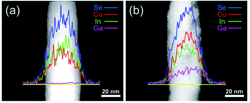 | ||
| Fig. 4 STEM and EDS line scan of (a) CuInSe2 and (b) CuIn0.61Ga0.39Se2 nanowires. | ||
The elemental distribution for CuIn0.61Ga0.39Se2 nanowires was verified through the element maps from EDS. It was obviously found that the Cu, In, Ga and Se elements were distributed throughout the nanowire, while Bi was limited to the tip of wire (Fig. 5).
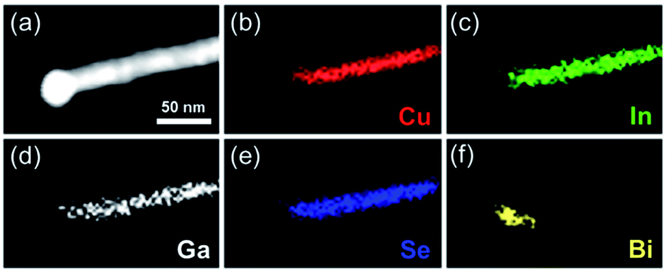 | ||
| Fig. 5 STEM and EDS elemental mapping of Cu, In, Ga, Se and Bi for CuIn0.61Ga0.39Se2 nanowires. | ||
PV devices were successfully produced using CuIn0.61Ga0.39Se2 NWs. Like CIS, CIGS thin films are p-type, and solar energy devices were assembled with a layered structure composed of Au/CIGS NWs/CdS/ZnO/indium tin oxide (ITO). The NW layer was fabricated by spray coating a toluene dispersion without annealing. Fig. 6 illustrates the PV response of a typical device having an open-circuit voltage (VOC) of 252 mV, a short-circuit current density (JSC) of 5.256 mA cm−2, a fill factor (FF) of 0.317, and a power conversion efficiency (PCE) of 0.421% under AM 1.5 conditions.
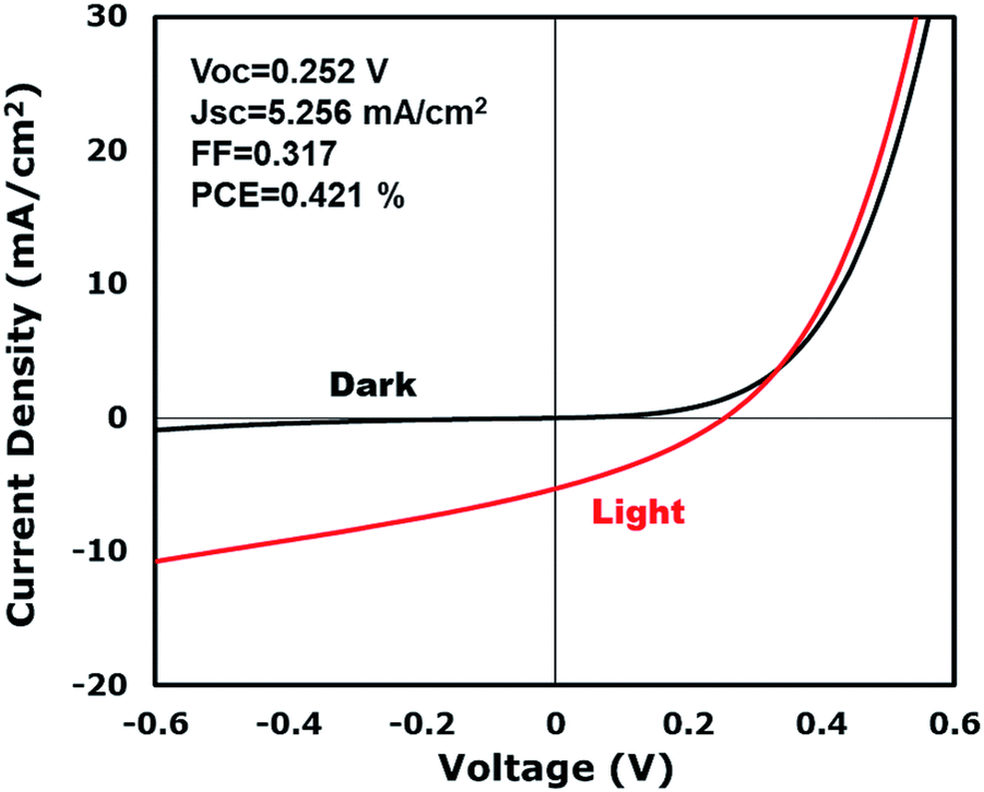 | ||
| Fig. 6 Current–voltage characteristics of a CuIn0.61Ga0.39Se2 NWs PV device. | ||
The PV response of the nanowire devices demonstrates a principle verification and provides the opportunity for application in solar energy. However, the intrinsic attributes of nanowire devices lead to a relatively poor performance. The lower shunt resistance caused by the voids in the nanowire film leads to low VOCs and FFs. Fig. 1e illustrates a TEM image of a nanowire film where the film is well-regulated. However, voids exist in the films and cause a lower shunt resistance when subjected to light irradiation. Nanowires are randomly deposited like a tangled mat and lay parallel to the electrode interface. Therefore, the optimization of the nanowire orientation requires further study. In order to obtain a better charge separation, one single nanowire should be spanned directly between the two electrodes, which requires the fabricated nanowires to be shorter. In addition, faults in the films and nanowires could also lead to poor device performances. Twinning nanowire lattices have been fabricated, which have disadvantages in carrier transport properties,31 and vacancies related to In insufficiency in the nanowires could also decrease the device performance. Practically, CIS nanowires are expected to be phase pure, twin-free, stoichiometric chalcopyrite crystals. However, the reaction temperature and presence of surfactants (such as HDA) have a substantial effect on the phase purity of the nanowires. Meanwhile, the reaction temperature, solvent or types of precursors also have an influence on the morphology, which demands in-depth optimization.
4. Conclusion
In conclusion, crystallized CIGS nanowires have been synthesized by cation exchange for the first time. This work describes the formation mechanism of CIGS using a heating-up process in OLA, which can be employed as a general method for in situ conversion of CIS to CIGS. A PV apparatus coated with CIGS NWs has shown PCEs as high as 0.421%. However, the reasons for low PCEs of solar cells were that high-temperature or chemical means had not been processed after deposition for the absorber layers. An increase in PV efficiency can be achieved by optimizing synthetic and fabrication processes. These CIGS nanowires as absorbing materials provide the opportunity for improving efficiency in solar energy applications. Meanwhile, CIGS nanowires can be employed by mixing them with other photovoltaic materials, such as nanocrystals or organics, for generating much more heterojunction equipment based on these nanowires.Conflicts of interest
There are no conflicts to declare.Acknowledgements
This research was funded by the Education Department of Henan Province (No. 20A430024), the National Key Research and Development Program of China (No. 2016YFB0301101), the Robert A. Welch Foundation (grant no. F-1464), the National Science Foundation through its Industry/University Cooperative Research Centers program (grant no. IIP-1134849), and CJS acknowledges funding by a National Science Foundation Graduate Research Fellowship (grant no. DGE-1110007).Notes and references
- A. Miller, A. Mackinnon and D. Weaire, Solid State Phys., 1982, 36, 119–175 Search PubMed.
- G. W. Jia and J. Du, Cryst. Growth Des., 2018, 18, 7489–7495 CrossRef CAS.
- G. W. Jia and J. Du, Inorg. Chem., 2018, 57, 14961–14966 CrossRef CAS.
- G. W. Jia and J. Du, Inorg. Chem., 2019, 58, 695–702 CrossRef CAS.
- M. G. Panthani, V. Akhavan, B. Goodfellow, J. P. Schmidtke, L. Dunn, A. Dodabalapur, P. F. Barbara and B. A. Korgel, J. Am. Chem. Soc., 2008, 130, 16770–16777 CrossRef CAS.
- S. J. Ahn, K. H. Kim and K. H. Yoon, Colloids Surf., A, 2008, 313, 171–174 CrossRef.
- G. Jia, B. Liu, K. Wang, C. Wang, P. Yang, J. Liu, W. Zhang, R. Li, S. Zhang and J. Du, Nanomaterials, 2019, 9, 409 CrossRef CAS.
- P. Jackson, D. Hariskos, E. Lotter, S. Paetel, R. Wuerz, R. Menner, W. Wischmann and M. Powalla, Prog. Photovolt. Res. Appl., 2011, 19, 894–897 CrossRef CAS.
- E. Wallin, U. Malm, T. Jarmar, O. L. M. Edoff and L. Stolt, Prog. Photovolt. Res. Appl., 2012, 20, 851–854 CrossRef CAS.
- I. Gur, N. A. Fromer, M. L. Geier and A. P. Alivisatos, Science, 2005, 310, 462–465 CrossRef CAS PubMed.
- Q. Guo, G. M. Ford, H. W. Hillhouse and R. Agrawal, Nano Lett., 2009, 9, 3060–3065 CrossRef CAS.
- Q. Guo, H. W. Hillhouse and R. Agrawal, J. Am. Chem. Soc., 2009, 131, 11672–11673 CrossRef CAS.
- G. I. Koleilat, L. Levina, H. Shukla, S. H. Myrskog, S. Hinds, A. G. Pattantyusabraham and E. H. Sargent, ACS Nano, 2008, 2, 830–840 CrossRef.
- J. J. Choi, Y. F. Lim, M. E. B. Santiagoberrios, M. Oh, B. R. Hyun, L. Sun, A. C. Bartnik, A. Goedhart, G. G. Malliaras and H. D. Abruña, Nano Lett., 2009, 9, 3749–3755 CrossRef CAS.
- H. W. Hillhouse and M. C. Beard, Curr. Opin. Colloid Interface Sci., 2009, 14, 245–259 CrossRef CAS.
- C. Steinhagen, V. A. Akhavan, B. W. Goodfellow, M. G. Panthani, J. T. Harris, V. C. Holmberg and B. A. Korgel, ACS Appl. Mater. Interfaces, 2011, 3, 1781–1785 CrossRef CAS.
- A. I. Hochbaum and P. Yang, Chem. Rev., 2010, 110, 527–546 CrossRef CAS.
- M. Law, L. E. Greene, J. C. Johnson, R. Saykally and P. Yang, Nat. Mater., 2005, 4, 455–459 CrossRef CAS.
- W. U. Huynh, J. J. Dittmer and A. P. Alivisatos, Science, 2002, 295, 2425–2427 CrossRef CAS.
- H. Peng, D. T. Schoen, S. Meister, X. F. Zhang and Y. Cui, J. Am. Chem. Soc., 2007, 129, 34–35 CrossRef CAS.
- S. H. Wei, S. B. Zhang and A. Zunger, Appl. Phys. Lett., 1998, 72, 3199–3201 CrossRef CAS.
- A. M. Gabor, J. R. Tuttle, D. S. Albin, M. A. Contreras, R. Noufi and A. M. Hermann, Appl. Phys. Lett., 1994, 65, 198–200 CrossRef CAS.
- H. Li, R. Brescia, M. Povia, M. Prato, G. Bertoni, L. Manna and I. Moreels, J. Am. Chem. Soc., 2013, 135, 12270–12278 CrossRef CAS.
- D. H. Son, S. M. Hughes, Y. Yin and A. A. Paul, Science, 2004, 306, 1009–1012 CrossRef CAS.
- B. J. Beberwyck and A. P. Alivisatos, J. Am. Chem. Soc., 2012, 134, 19977–19980 CrossRef CAS.
- S. Deka, K. Miszta, D. Dorfs, A. Genovese, G. Bertoni and L. Manna, Nano Lett., 2010, 10, 3770–3776 CrossRef CAS.
- S. E. Wark, C. H. Hsia and D. H. Son, J. Am. Chem. Soc., 2008, 130, 9550–9555 CrossRef CAS.
- J. M. Pietryga, D. J. Werder, D. J. Williams, J. L. Casson, R. D. Schaller, V. I. Klimov and J. A. Hollingsworth, J. Am. Chem. Soc., 2008, 130, 4879–4885 CrossRef CAS.
- C. Dong and F. C. van Veggel, ACS Nano, 2009, 3, 123–130 CrossRef CAS.
- W. H. Hsu, H. I. Hsiang, Y. L. Chang, D. T. Ray and F. S. Yen, J. Am. Chem. Soc., 2011, 94, 3030–3034 CAS.
- J. H. Kang, Y. Myung, W. C. Jin, M. J. Dong, W. L. Chi, J. Park and E. H. Cha, J. Mater. Chem., 2012, 22, 8413–8419 RSC.
Footnotes |
| † Electronic supplementary information (ESI) available. See DOI: 10.1039/c9ra04605d |
| ‡ These authors contributed equally to this work. |
| This journal is © The Royal Society of Chemistry 2019 |