
 Open Access Article
 This Open Access Article is licensed under a Creative Commons Attribution-Non Commercial 3.0 Unported Licence
Inkjet assisted fabrication of planar biocompatible memristors
Georgii A. Illarionov a,
Denis S. Kolchanova,
Oleg A. Kuchura,
Mikhail V. Zhukovab,
Ekaterina Sergeevaa,
Vladimir V. Krishtopac,
Alexandr V. Vinogradova and
Maxim I. Morozov*a
a,
Denis S. Kolchanova,
Oleg A. Kuchura,
Mikhail V. Zhukovab,
Ekaterina Sergeevaa,
Vladimir V. Krishtopac,
Alexandr V. Vinogradova and
Maxim I. Morozov*a
aLaboratory of Solution Chemistry of Advanced Materials and Technologies, ITMO University, Lomonosova str. 9, St. Petersburg, 191002, Russia. E-mail: maximm@alumni.ntnu.no; morozov@scamt-itmo.ru
bInstitute for Analytical Instrumentation RAS, Ivan Chernykh str. 31-33, St. Petersburg, 198095, Russia
cResearch Center, Ivanovo State Medical Academy, Sheremetevsky ave. 8, Ivanovo, 153012, Russia
First published on 5th November 2019
Abstract
In this study we address a novel design of a planar memristor and investigate its biocompatibility. An experimental prototype of the proposed memristor assembly has been manufactured using a hybrid nanofabrication method, combining sputtering of electrodes, patterning the insulating trenches, and filling them with a memristive substance. To pattern the insulating trenches, we have examined two nanofabrication techniques employing either a focused ion beam or a cantilever tip of an atomic force microscope. Inkjet printing has been used to fill the trenches with the functional titania ink. The experimental prototypes have qualitatively demonstrated memristive current–voltage behavior, as well as high biocompatibility.
Introduction
Memristors are passive two-terminal elements of an electric circuit, whose resistance depends on the previously passed electric current. Their history started from the prediction of a hypothetically “missing circuit element” by Leon Chua in 19711 and nowadays has reached a slightly revised concept, basically meaning “the resistance switching memory”.2 The memory effect of resistive switching is observed in many organic and inorganic nanomaterials, including simple oxides and their modifications.3–7 This allows integration of memristors into micro- and nanoelectronic devices using traditional nanofabrication techniques.8–10 Nowadays, memristors are considered to be one of the key elements of newly developing neuromorphic electronics,11,12 since it functionally mimics the synaptic plasticity of biological neurons13–15 and thus is suitable for bioinspired technologies.14,16,17Neuromorphic electronics was triggered by the discovery of principal electric phenomena in a neuron cell membrane in the early 1950's. In particular, the resistive switching model of the voltage gated ionic channels described by Hodgkin and Huxley in their Nobel prize awarded research15 gave rise to numerous electrical and computational prototypes of neural networks that were known since early 1960's.18,19 Nowadays, there is a growing interest in functional interfaces between biological and artificial neural networks. This interest arises from two general research trends: adapting digital computational processes to native information processing mechanisms20,21 and investigation of the functional reserves of the biological neural networks.22,23 From the technological point of view, the electronic resistive switching memory is the common feature belonging to both biological and artificial electrical neurons. As such, it is considered as the frontier of feasible bionanointerfaces. The state of the art and future expectations in this field have recently been outlined in a topical review.24
Nowadays, in vitro studies of electrical activity in neuronal and other biological cells require special microelectrode arrays25 and thus external wiring is needed to establish connection with a control unit or a memristive device.26 Alternatively, microelectrodes and memristive elements can be integrated into one device. In the most common topological arrangement, memristors are fabricated as a dielectric thin film sandwiched between the transverse arrays of top and bottom electrodes (so-called “crossbar latch”). This configuration is a key architecture proposed for integrated nanoscale electronics.27 Integration of crossbar memristors with the outer microelectrode array for in vitro experiments with biological cells or tissues would require an additional insulating layer and conductive channels between the inner and outer electrodes. This can be fabricated using conventional lithography. Alternatively, a layout with planar topology can be designed. Recently, several studies addressed the planar configuration of memristive elements.28–30 These elements were technologically performed using photolithography, leaving gaps between the pairs of metallic electrodes and filling them with a memristive composite. The gaps widths were reported to range from 10 μm![[thin space (1/6-em)]](https://www.rsc.org/images/entities/char_2009.gif) 28,29 to 50–200 μm.30 To achieve the memristive effect between so far distant electrodes, the authors used dielectric nanocomposite materials with silver nanoparticles. The use of silver nanoclusters allows for memristive effect based on reversible generation of conductive filaments through the electrically induced diffusive mechanism.31 However, the use of silver nanoparticles in biocompatible devices is risky, as their reported cytotoxicity at the cell level may be an issue.32 In this regard, an interesting solution would be the use of other than silver-based compounds with metal nanoclusters capable for realizing the same type of diffusive mechanism of memristivity. Recently, a promising effect of electroforming in gold nanoclusters has been demonstrated on a planar memristor prototype (3 mm × 3 mm) fabricated by supersonic cluster beam deposition.33
28,29 to 50–200 μm.30 To achieve the memristive effect between so far distant electrodes, the authors used dielectric nanocomposite materials with silver nanoparticles. The use of silver nanoclusters allows for memristive effect based on reversible generation of conductive filaments through the electrically induced diffusive mechanism.31 However, the use of silver nanoparticles in biocompatible devices is risky, as their reported cytotoxicity at the cell level may be an issue.32 In this regard, an interesting solution would be the use of other than silver-based compounds with metal nanoclusters capable for realizing the same type of diffusive mechanism of memristivity. Recently, a promising effect of electroforming in gold nanoclusters has been demonstrated on a planar memristor prototype (3 mm × 3 mm) fabricated by supersonic cluster beam deposition.33
The micrometer-scale resolution for the planar patterning of the diffusive-type memristors can be achieved by the conventional mask lithography. The use of mask lithography is however limited for in situ biological studies, so all the operations are allowed only prior to deposition of biological cells.
An alternative choice of planar memristive elements is represented by various metal oxides, whose memristance is based on the ionic drift mechanism.4,34–36 However, their realization requires much thinner dielectric layer, as the theoretical memristance of the ionic drift system is shown to be inverse square dependent on the distance between the electrodes.4 In this case, however, the use of conventional mask lithography meets aberration challenges and thus becomes costly.
In this study, we propose a hybrid nanofabrication method for planar memristors, comprising the nanoscale patterning of insulating trenches by atomic force microscopy (AFM) and inkjet printing of the functional ink. This combination allows accurate manipulations at ambient environment and as such is prospective for designing, engineering, and prototyping electrical circuits with biological cells or tissues, both prior to and after their deposition. A prototype device with a series of memristor elements has been manufactured accordingly and thoroughly investigated. In order to investigate the biocompatibility of the materials used in the prototype, an assay for their biocompatibility has been performed using both neuronal (IMR-32, neuroblastoma) and non-neuronal (PHF, postnatal human fibroblasts) cell lines. Next, we report the main processing features for the elaborated prototype, the functional behaviour, and discuss the applicability, challenges, and further prospects of the proposed fabrication technique.
Materials and methods
Device outline
The concept of the proposed planar memristor element is as follows: a thin layer of metallic electrode is deposited on a glass substrate. The shape of the electrode has a narrow bottleneck area in the middle, where a thin trench across the electrode is formed. The depth of the trench overcomes the electrode thickness, so that the resulting narrow gap splits the original electrode into two terminals. Then the gap is filled by a memristive dielectric substance.In our prototype samples, five memristor elements with planar Au–TiO2–Au sandwiches were fabricated on the surface of glass substrates (size 76 mm × 25 mm × 1 mm, roughness <0.15 μm, Levenhuk, Russia). The electrodes were deposited by gold sputtering, while their shapes were profiled by photolithography. The electrode separating trenches were made by scratching with a cantilever tip of an atomic force microscope (AFM). In addition, a reference series of memristive elements were prepared with trenches made by focused ion beam (FIB) milling. The resulting gaps between the electrodes were filled with titanium dioxide ink, using a laboratory scale inkjet printer. The AFM-based fabrication process is schematically shown in Fig. 1. In the following subsections, the main processing steps will be described in detail.
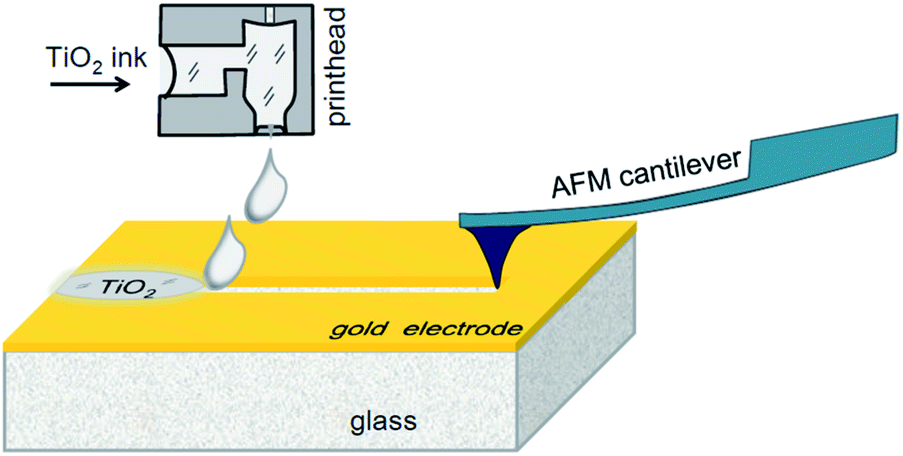 | ||
| Fig. 1 Scheme for hybrid fabrication of a planar memristor. | ||
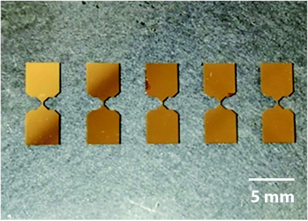 | ||
| Fig. 2 Gold-sputtered electrodes. | ||
The trenches of the first type were made mechanically, by scratching the gold surface with a cantilever tip of a scanning probe microscope (SPM) Ntegra Aura (NT-MDT, Russia), operating in the AFM contact mode. The cantilever was chosen with a hardness of 22 N m−1 (NT-MDT, Russia) and a tip curvature radius of 10 nm. The scratching force was estimated as:
| F = ΔZk |
The trenches of the second type were etched by a focused ion beam of Ga using a Carl Zeiss Neon 40 Cross-Beam workstation. Acceleration voltage and current in the beam column were 30 kV and 10 pA, correspondingly.
The synthesized sol was processed in a rotary evaporator until the solid TiO2 phase was obtained. Then the ink was derived by diluting TiO2 nanoparticles in deionized water and adding ethylene glycol and a surfactant DX4000 in order to adjust the surface tension and viscosity of the ink solution. The ink rheological properties were adjusted to comply with the technological printing environment (the printhead nozzle diameter and the desirable droplet volume).
The phase composition and crystallinity of the prepared titania ink were characterized by X-ray diffraction and gas sorption methods, using a Rigaku SmartLab 3 diffractometer (CuKα radiation, λ = 1.5418 Å) and a Quantachrome Nova 1200e surface area analyser, respectively. The surface area and the average pore diameters were estimated using the models by Brunauer–Emmett–Teller (BET) and Barrett–Joyner–Halenda, (BJH) respectively.
The prepared TiO2 ink was decanted into a cartridge and inkjet deposited onto the trenches by inkjet printing. A Fujifilm Dimatix materials printer DMP-2831 with a 10 pL cartridge was used. The printing conditions were set as follows: temperature of the substrate 35 °C, nozzle driving voltage 22 mV, drop spacing 25 μm, and 1 mm sample-to-printhead distance.
Characterization
The quality of trench forming was controlled by the means of atomic force microscopy (AFM) and scanning electron microscopy (SEM), while the final device prototypes were subjected to electric characterization, as well as to cell viability assay, using the standard methylthiazol tetrazolium (MTT) test protocol.An additional visualization of microstructure was obtained using a scanning electron microscope (SEM) Tescan Vega 3 with a beam accelerating voltage of 20 kV, operating with a secondary electron detector.
Results and discussion
Topology
Profiling of the trench by an AFM cantilever tip requires adjustment of scratching force and speed towards the optimal regime. In this study we have investigated the relationships between the applied scratching force and the profile of the resulting trench in the gold layer. The results are shown in Fig. 3. Fig. 3a illustrates the AFM images for a series of trenches obtained at forces of 2, 5, 8, 12, 15, and 20 μN, while the corresponding depth profiles are shown in Fig. 3b. The topology parameters of obtained trenches are listed in Table 1. The results demonstrate that the scratching efficiency changes drastically when the applied force is sufficient to break through the whole layer. In the case of 30 nm gold film, this was achieved at 20 μN.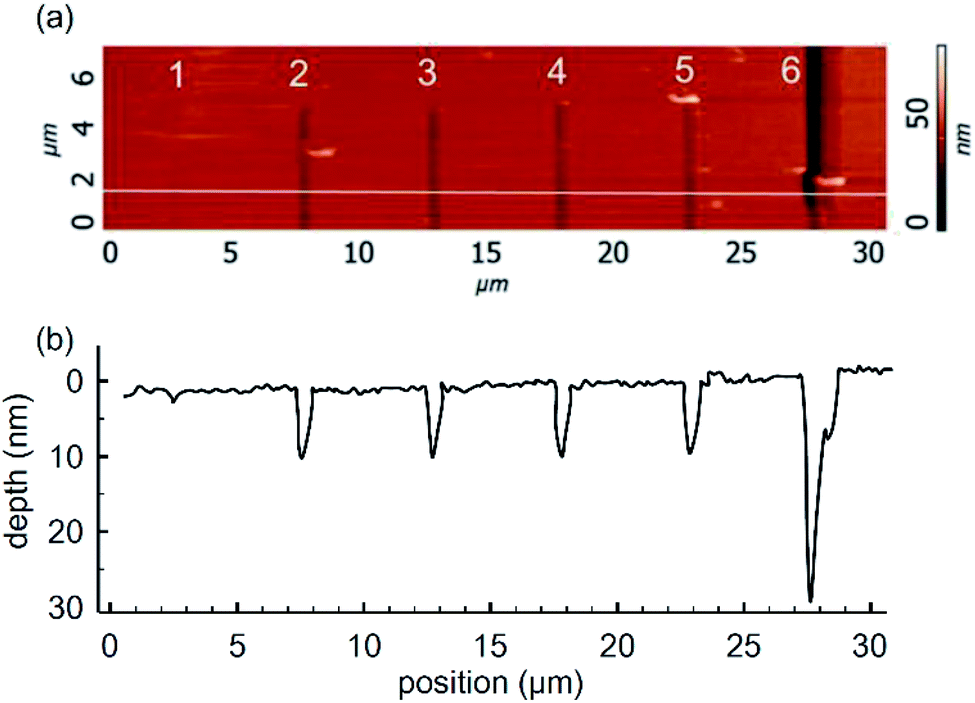 | ||
| Fig. 3 (a) AFM images of trenches formed with cantilever forces of 2, 5, 8, 12, 15, and 20 μN; and (b) the corresponding depth profiles. | ||
| Scratch number, Fig. 3a | Force, μN | Width at middle, nm | Depth, nm |
|---|---|---|---|
| 1 | 2 | 300 ± 100 | 1.5 ± 0.5 |
| 2 | 5 | 400 ± 100 | 8.5 ± 0.5 |
| 3 | 8 | 400 ± 100 | 8.5 ± 0.5 |
| 4 | 12 | 500 ± 100 | 8.5 ± 0.5 |
| 5 | 15 | 500 ± 100 | 8.5 ± 0.5 |
| 6 | 20 | 500 ± 100 | 30.0 ± 2.0 |
The optimal scratching speed of 3 μm s−1 has been found empirically. At a higher speed, scratching was accompanied with a ploughing effect, while speed lowering only resulted in longer processing time.
Fig. 4 compares the trenches obtained by AFM scratching (Fig. 4a) and FIB etching (Fig. 4b). It is noteworthy that the shape of the AFM-processed trench is strongly affected by the geometry of the cantilever tip, so that it is narrow at the bottom (ca. 150–200 nm) and broadening towards the top (ca. 700–800 nm). In contrast, the FIB-etched trench has regular rectangularly shaped profile, ca. 400 nm width (Fig. 4b).
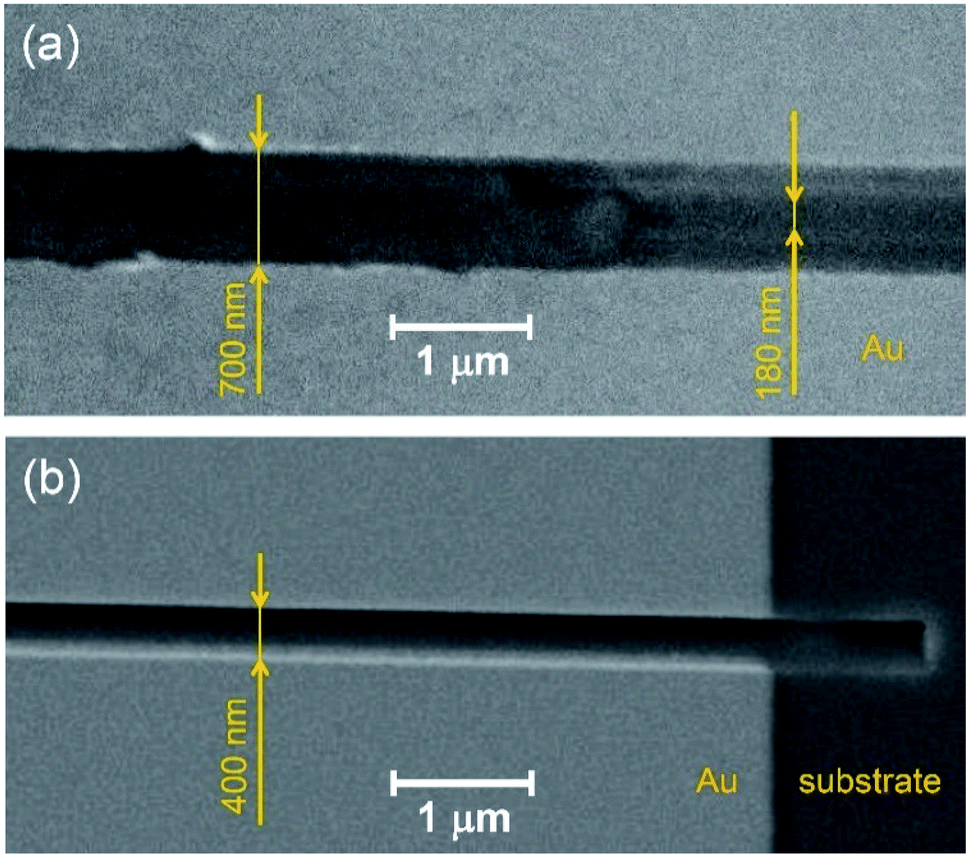 | ||
| Fig. 4 SEM images of trenches prepared by (a) AFM scratching and (b) FIB etching. | ||
Dielectric layer
Sol–gel synthesis of TiO2 nanoparticles is a low temperature process with a possibility to control the phase ratio of different polymorphs as well as the morphology by adjusting parameters of acidic peptization in an aqueous solution.39 In this study we used the regime of synthesis previously adjusted to meet the rheological requirements for inkjet printing.38,43 XRD pattern of the derived ink is shown in Fig. 5. The synthesized nanoparticles are predominantly identified as anatase (JSPDS card #21-1272), while some traces of brookite have also been detected (JSPDS card #29-1360); no rutile (JSPDS card #21-1276) is observed. Anatase is the well suitable TiO2 polymorph for memristive application that has been demonstrated in a series of theoretical44 and experimental45–47 studies. The average crystallite size by Scherer's equation was ca. 6 nm upon heat treatment at 50 °C and ca. 7 nm after treatment at 200 °C. The BET surface area was evaluated as 159 m2 g−1 and 144 m2 g−1 with the BJH average pore diameters 3.2 nm and 3.5 nm for the samples treated at 50 °C and 200 °C, respectively.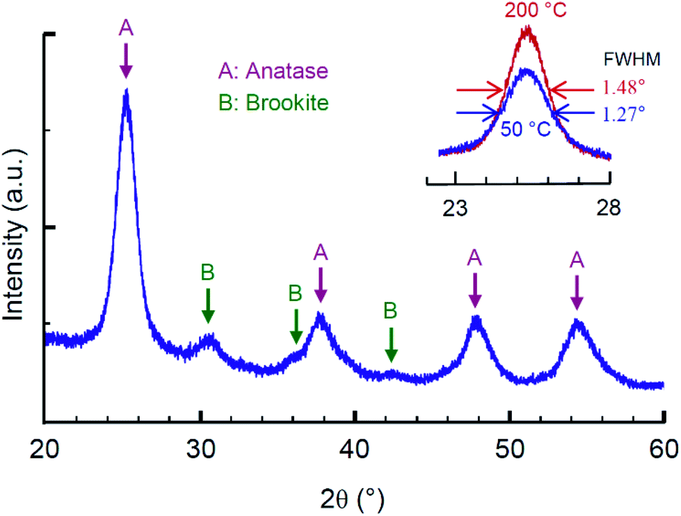 | ||
| Fig. 5 XRD pattern for sol–gel derived TiO2 ink; the inset shows peaks for materials thermally annealed at 50 °C and 200 °C. | ||
Fig. 6 demonstrates the result of trench filling by inkjet deposition, followed by annealing. As visible in Fig. 6a, the titania ink droplets are deposited precisely on the trenches. The SEM image shown in Fig. 6b demonstrates the droplet morphology. It forms a compact film with little roughness.
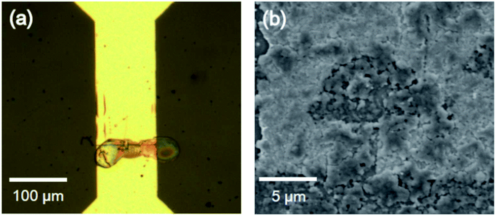 | ||
| Fig. 6 Images of TiO2 droplets deposited on trench: (a) optical microscopy; and (b) SEM. | ||
Electric characterization
The planar Au/TiO2/Au memristors were characterized by current–voltage dependencies at several measurement cycles with stepwise increasing and decreasing driving voltage. The results are shown in Fig. 7. All the memristive elements demonstrated rather very low current response, ranging from a few to hundreds nanoamperes, which may be a result of incomplete or loose filling of the narrow trenches with TiO2 ink and the relatively low crystallinity of titania. Despite this, the U-I dependencies demonstrate the qualitatively memristive behaviour with gradually increasing conductivity at each subsequent unipolar cycle of the applied dc voltage. No electric response was detected prior to filling the trench with titania ink. The threshold voltages igniting the memristive potentiation were 4.2 V in the case of AFM-made trench (Fig. 7a) and 3.0 V in the case of FIB-made trench (Fig. 7b), which correspond to the difference in their widths (Fig. 4a and b). Owing to proper rectangular shape of the FIB-made trench, the threshold potentiation electric field can be calculated and is thus evaluated as 75 kV cm−1.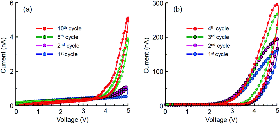 | ||
| Fig. 7 Current–voltage potentiation curves for a sequence of unipolar cycles applied to memristors prepared with: (a) AFM-scratched trench and (b) FIB-etched trench. | ||
Biocompatibility
The fabrication method proposed in this study implies deposition of Au and TiO2 on the substrate surface. In order to assess biocompatibility of all the materials, they have been deposited separately on a series of glass substrates and subjected to MTT cytotoxicity assays using IMR-32 and PHF cell lines. The experimental results are shown in Fig. 8. The diagram of cell viability is shown in Fig. 8a and demonstrates that none of the materials caused any notable cytotoxic effect on the IMR-32 and PHF cells. Indeed, the cell survival rates for IMR-32 and PHF on Au and TiO2 were 97.37% for IMR-32/TiO2, 95.86% for PHF/TiO2, 95.93% for IMR-32/Au, and 95.05% for PHF/Au with respect to the control solely incubated batch. In this assay, all the cells were cultivated for 72 hours, the time sufficient for 3 cycles of cell divisions, and no apparent morphological or metabolic changes have been observed, as illustrated in Fig. 8b–e for all the combinations of the cells and materials addressed in the study. Thus, the memristor elements fabricated by the proposed hybrid planar technology and using Au and TiO2 as constituting materials have demonstrated high biocompatibility.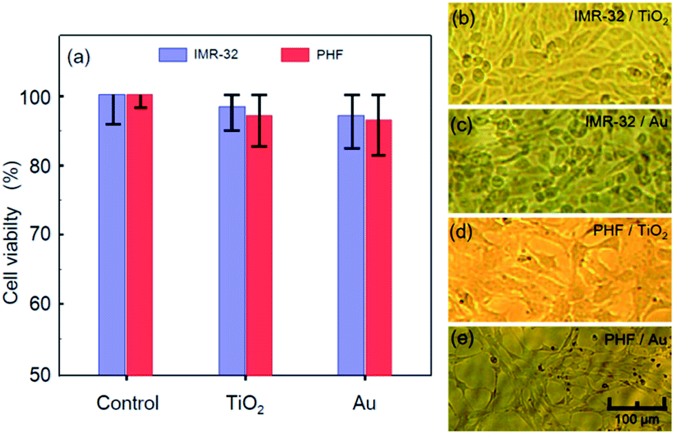 | ||
| Fig. 8 Viability of IMR-32 and PHF cells incubated solely (control) and on substrates of TiO2 and Au: (a) chart for percentage of viable cells; and (b–e) optical microscope images of cells after 72 hours of incubation: (b) IMR-32 on TiO2, (c) IMR-32 on Au, (d) PHF on TiO2, and (e) PHF on Au. | ||
Discussion
The fabrication method addressed in this study has a limited range of applicability, though it has certain favourable advantages for designing in vitro experiments with biological tissues and cells at the lab scale. Indeed, the atomic force microscopy is a well-recognized tool for nanoscale materials patterning and engineering,48,49 just as much as for bioengineering, investigations in biochemistry and cell biology.50,51 Inkjet printing is a cost-efficient nanofabrication method, especially for the lab-scale prototyping.52,53 It typically operates with a picolitre droplet volume and 10–20 μm spatial resolution52 of the droplet depositing. This is sufficient for integration of the printable microcircuits with biological cells, as long as the cell sizes (ca. 100 μm, e.g. Fig. 8d and e) surpass the printing resolution limit. Furthermore, the inkjet bioprinting is rapidly developing nowadays,54,55 thus enabling precise positioning and arrangement of biological and inorganic elements on the substrate.The nano- and microfabrication methods based on physical (FIB)56 or chemical (mask lithography)28,29 treatment provide better reproducibility,52 though they cannot be considered for conducting in situ experiments with biological cells or tissues. In these cases, the combination of AFM and inkjet patterning shall be a justified choice. Their combination allows for in situ circuit manipulations even in the case with the integrated biological substances.
Seemingly, the major challenge in the proposed design of planar memristors is the relatively low current response experimentally achieved at this stage (Fig. 7a). Nonetheless, we believe that further development of the functional inks shall lead to better performance. Firstly, a more careful adjustment of the ink crystallinity is needed. Technologically, it is feasible for sol–gel38,57 and other58 processing routes. Secondly, as the concentration of oxygen vacancies in the functional layer significantly affects the memristive performance,44 the optimal level of oxygen nonstoichiometry can be achieved by an appropriate doping or by thermal treatment in an inert atmosphere. And thirdly, other biocompatible memristive compositions can be considered besides TiO2.
Conclusion
In summary, we have designed, fabricated, and investigated a novel planar configuration of a memristive element. The proposed hybrid nanofabrication method allows patterning the insulating trenches in the gold-sputtered electrodes and filling them with functional inks using the AFM and inkjet printing techniques, correspondingly. The combination of these methods allows for operational versatility for designing in vitro experiments with biological cells and tissues. The fabricated planar memristors have demonstrated a memristive behaviour qualitatively, upon U-I characterization. However the electrical response was rather week, possibly due to incomplete filling of the trench or low density of the filling material. Thus the proposed fabrication technique requires further elaboration. Finally, the materials used in the fabrication have demonstrated reasonable biocompatibility, not causing any apparent cytotoxic effect on IMR-32 and PHF cells.Conflicts of interest
There are no conflicts to declare.Acknowledgements
The research has been carried out with financial support from the Russian Science Foundation (Project No 19-19-00433). AVV acknowledges the scholarship of the President of the Russian Federation (SP-1158.2019.1). The authors acknowledge the Engineering Center at the Saint-Petersburg State Technological Institute (Technical University) for the support with X-Ray diffraction analysis.References
- L. O. Chua, IEEE Trans. Circuit Theory, 1971, 18, 507–519, DOI:10.1109/TCT.1971.1083337.
- L. O. Chua, Appl. Phys. A, 2011, 102, 765–783, DOI:10.1007/s00339-011-6264-9.
- W. Lu, D. S. Jeong, M. Kozicki and R. Waser, MRS Bull., 2012, 37, 124–130, DOI:10.1557/mrs.2012.5.
- D. B. Strukov, G. S. Snider, D. R. Stewart and R. S. Williams, Nature, 2008, 453, 80–83, DOI:10.1038/nature06932.
- J. J. Yang, F. Miao, M. D. Pickett, D. A. A. Ohlberg, D. R. Stewart, C. N. Lau and R. S. Williams, Nanotechnology, 2009, 20, 215201, DOI:10.1088/0957-4484/20/21/215201.
- Y. Yang, P. Gao, S. Gaba, T. Chang, X. Pan and W. Lu, Nat. Commun., 2012, 3, 732, DOI:10.1038/ncomms1737.
- L. Wang, C. H. Yang, J. Wen, S. Gai and Y. X. Peng, J. Mater. Sci.: Mater. Electron., 2015, 26, 4618–4628, DOI:10.1007/s10854-015-2848-z.
- Q. Xia, W. Wu, G. Y. Jung, S. Pi, P. Lin, Y. Chen, X. Li, Z. Li, S. Y. Wang and R. S. Williams, Appl. Phys. A: Mater. Sci. Process., 2015, 121, 467–479, DOI:10.1007/s00339-015-9038-y.
- S. Barcelo and Z. Li, Nano Convergence, 2016, 3, 21, DOI:10.1186/s40580-016-0081-y.
- Q. Xia, W. Robinett, M. W. Cumbie, N. Banerjee, T. J. Cardinali, J. J. Yang, W. Wu, X. Li, W. M. Tong, D. B. Strukov, G. S. Snider, G. Medeiros-Ribeiro and R. S. Williams, Nano Lett., 2009, 9, 3640–3645, DOI:10.1021/nl901874j.
- J. P. Strachan and W. D. Lu, Nat. Electron., 2018, 1, 22–29, DOI:10.1038/s41928-017-0006-8.
- J. J. Yang, D. B. Strukov and D. R. Stewart, Nat. Nanotechnol., 2013, 8, 13–24, DOI:10.1038/nnano.2012.240.
- L. O. Chua and S. M. Kang, Proc. IEEE, 1976, 64, 209–223, DOI:10.1109/PROC.1976.10092.
- Z. H. Tan, X. B. Yin, R. Yang, S. B. Mi, C. L. Jia and X. Guo, Sci. Rep., 2017, 7, 713, DOI:10.1038/s41598-017-00849-7.
- A. L. Hodgkin and A. F. Huxley, J. Physiol., 1952, 117, 500–544, DOI:10.1113/jphysiol.1952.sp004764.
- C. Li, D. Belkin, Y. Li, P. Yan, M. Hu, N. Ge, H. Jiang, E. Montgomery, P. Lin, Z. Wang, W. Song, J. P. Strachan, M. Barnell, Q. Wu, R. S. Williams, J. J. Yang and Q. Xia, Nat. Commun., 2018, 9, 2385, DOI:10.1038/s41467-018-04484-2.
- S. Liu, Y. Wang, M. Fardad and P. K. Varshney, IEEE Circuits Syst. Mag., 2018, 18, 29–44, DOI:10.1109/MCAS.2017.2785421.
- B. Widrow, “An adaptive Adaline neuron using chemical memristors”, Stanford Univ., TR, 1960, pp. 1553–2 Search PubMed.
- B. Widrow, ARS J., 1962, 32, 1378–1385, DOI:10.2514/8.6293.
- B. Yazmir and M. Reiner, Neuroscience, 2018, 378, 100–112, DOI:10.1016/j.neuroscience.2016.10.060.
- J. J. Daly and J. E. Huggins, Arch. Phys. Med. Rehabil., 2015, 96, S1–S7, DOI:10.1016/j.apmr.2015.01.007.
- J. J. S. Norton, J. Mullins, B. E. Alitz and T. Bretl, J. Neural Eng., 2018, 15, 056012, DOI:10.1088/1741-2552/aacfdd.
- M. Takemi, T. Maeda, Y. Masakado, H. R. Siebner and J. Ushiba, Neuroimage, 2018, 183, 597–605, DOI:10.1016/j.neuroimage.2018.08.070.
- A. Chiolerio, M. Chiappalone, P. Ariano and S. Bocchini, Front. Neurosci., 2017, 11, 70, DOI:10.3389/fnins.2017.00070.
- P. Massobrio, J. Tessadori, M. Chiappalone and M. Ghirardi, Neural Plast., 2015, 2015, 1–18, DOI:10.1155/2015/196195.
- D. Gater, A. Iqbal, J. Davey and E. Gale, in IEEE 20th International Conference on Electronics, Circuits, and Systems (ICECS), IEEE, 2013, pp. 534–537, DOI:10.1109/ICECS.2013.6815469.
- P. J. Kuekes, D. R. Stewart and R. S. Williams, J. Appl. Phys., 2005, 97, 034301, DOI:10.1063/1.1823026.
- K. Rajan, S. Bocchini, A. Chiappone, I. Roppolo, D. Perrone, K. Bejtka, C. Ricciardi, C. F. Pirri and A. Chiolerio, Microelectron. Eng., 2017, 168, 27–31, DOI:10.1016/j.mee.2016.10.004.
- K. Rajan, S. Bocchini, A. Chiappone, I. Roppolo, D. Perrone, M. Castellino, K. Bejtka, M. Lorusso, C. Ricciardi, C. F. Pirri and A. Chiolerio, Flexible Printed Electron., 2017, 2, 024002, DOI:10.1088/2058-8585/aa64be.
- E. J. Sandouk, J. K. Gimzewski and A. Z. Stieg, Sci. Technol. Adv. Mater., 2015, 16, 045004, DOI:10.1088/1468-6996/16/4/045004.
- Z. Wang, S. Joshi, S. E. Savel’ev, H. Jiang, R. Midya, P. Lin, M. Hu, N. Ge, J. P. Strachan, Z. Li, Q. Wu, M. Barnell, G.-L. Li, H. L. Xin, R. S. Williams, Q. Xia and J. J. Yang, Nat. Mater., 2017, 16, 101–108, DOI:10.1038/nmat4756.
- T. Zhang, L. Wang, Q. Chen and C. Chen, Yonsei Med. J., 2014, 55, 283–291, DOI:10.3349/ymj.2014.55.2.283.
- C. Minnai, A. Bellacicca, S. A. Brown and P. Milani, Sci. Rep., 2017, 7, 7955, DOI:10.1038/s41598-017-08244-y.
- R. Waser and M. Aono, Nat. Mater., 2007, 6, 833–840, DOI:10.1038/nmat2023.
- D.-H. Kwon, et al., Nat. Nanotechnol., 2010, 5, 148–153, DOI:10.1038/nnano.2009.456.
- A. Wedig, et al., Nat. Nanotechnol., 2016, 11, 67–74, DOI:10.1038/nnano.2015.221.
- J. E. Sader, J. W. M. Chon and P. Mulvaney, Rev. Sci. Instrum., 1999, 70, 3967, DOI:10.1063/1.1150021.
- A. V. Yakovlev, V. A. Milichko, V. V. Vinogradov and A. V. Vinogradov, ACS Nano, 2016, 10, 3078–3086, DOI:10.1021/acsnano.5b06074.
- A. V. Vinogradov and V. V. Vinogradov, J. Am. Ceram. Soc., 2014, 97, 290–294, DOI:10.1111/jace.12560.
- N. Samardzic, M. Mionic, B. Dakic, H. Hofmann, S. Dautovic and G. Stojanovic, IEEE Trans. Electron Devices, 2015, 62, 1898–1904, DOI:10.1109/Ted.2015.2421283.
- C. Leyva-Porras, A. Toxqui-Teran, O. Vega-Becerra, M. Miki-Yoshida, M. Rojas-Villalobos, M. García-Guaderrama and J. A. Aguilar-Martínez, J. Alloys Compd., 2015, 647, 627–636, DOI:10.1016/j.jallcom.2015.06.041.
- T. Mosmann, J. Immunol. Methods, 1983, 65, 55–63, DOI:10.1016/0022-1759(83)90303-4.
- A. V. Yakovlev, V. A. Milichko, V. V. Vinogradov and A. V. Vinogradov, Adv. Funct. Mater., 2015, 25, 7375–7380, DOI:10.1002/adfm.201503483.
- A. Paris and S. Taioli, J. Phys. Chem. C, 2016, 120(38), 22045–22053, DOI:10.1021/acs.jpcc.6b07196.
- V. Prusakova, C. Collini, M. Nardi, R. Tatti, L. Lunelli, L. Vanzetti, L. Lorenzelli, G. Baldi, A. Chiappini, A. Chiasera, D. Ristic, R. Verucchi, M. Bortolottia and S. Dirè, RSC Adv., 2017, 7, 1654, 10.1039/C6RA25618J.
- N. Samardzić, M. Mionić, B. Dakić, H. Hofmann, S. Dautović and G. Stojanović, IEEE Trans. Electron Devices, 2015, 62(6), 1898–1904, DOI:10.1109/TED.2015.2421283.
- N. Duraisamy, N. Muhammad, H.-C. Kim, J.-D. Jo and K.-H. Choi, Thin Solid Films, 2012, 520, 5070–5074, DOI:10.1016/j.tsf.2012.03.003.
- G. Liu, M. Hirtz, H. Fuchs and Z. Zheng, Small, 2019, 1900564, DOI:10.1002/smll.201900564.
- X. N. Xie, H. J. Chung, C. H. Sow and A. T. S. Wee, Mater. Sci. Eng., R, 2006, 54, 1–48, DOI:10.1016/j.mser.2006.10.001.
- J. L. Toca-Herrera, ChemSusChem, 2019, 12, 603, DOI:10.1002/cssc.201802383.
- M. Li, N. Xi, Y. Wang and L. Liu, Nano Res., 2019, 12, 703, DOI:10.1007/s12274-018-2260-0.
- E. Menard, M. A. Meitl, Y. Sun, J.-U. Park, D. J.-L. Shir, Y.-S. Nam, S. Jeon and J. A. Rogers, Chem. Rev., 2007, 107, 1117–1160, DOI:10.1021/cr050139y.
- L. Nayak, S. Mohanty, S. Nayak and A. Ramadoss, J. Mater. Chem. C, 2019, 7, 8771, 10.1039/c9tc01630a.
- A. K. Miri, I. Mirzaee, S. Hassan, S. M. Oskui, D. Nieto, A. Khademhosseini and Y. S. Zhang, Lab Chip, 2019, 19, 2019–2037, 10.1039/c8lc01037d.
- R. Zimmermann, C. Hentschel, F. Schrön, D. Moedder, T. Büttner, P. Atallah, T. Wegener, T. Gehring, S. Howitz, U. Freudenberg and C. Werner, Biofabrication, 2019, 11, 045008, DOI:10.1088/1758-5090/ab2aa1.
- V. I. Avilov, O. A. Ageev, I. L. Jityaev, A. S. Kolomiytsev and V. A. Smirnov, Proc. SPIE, 2016, 10224, DOI:10.1117/12.2267084.
- E. Cerro-Prada, S. García-Salgado, M. Á. Quijano and F. Varela, Nanomaterials, 2019, 9, 26, DOI:10.3390/nano9010026.
- M. Zimmermann, B. Temel and G. Garnweitner, Chem. Eng. Process., 2013, 74, 83–89, DOI:10.1016/j.cep.2013.08.001.
| This journal is © The Royal Society of Chemistry 2019 |