
 Open Access Article
 This Open Access Article is licensed under a Creative Commons Attribution-Non Commercial 3.0 Unported Licence
Low-cost uncooled MWIR PbSe quantum dots photodiodes
Jijun Qiu†
*,
Binbin Weng†,
Lance L. McDowell and
Zhisheng Shi *
*
School of Electrical and Computer Engineering, University of Oklahoma, Norman, Oklahoma 73019, USA. E-mail: jjqiu@dlut.edu.cn; shi@ou.edu
First published on 23rd December 2019
Abstract
A mid-wave infrared (MWIR) uncooled PbSe-QDs/CdS p–n heterojunction photodiode has been fabricated using a wet-chemical synthesis route. This offers a low-cost alternative to traditional monocrystalline photodiodes relying on molecular beam epitaxy (MBE) technology. It was demonstrated that the post-annealing is critical to tailor the photoresponse wavelength and to improve the performance of photodiodes. After annealing at 673 K in air for 0.5 h, the ligand-free PbSe-QDs/CdS photodiode exhibits a MWIR spectral photoresponse with a cutoff wavelength of 4.2 μm at room temperature. Under zero-bias photovoltaic mode, the peak responsivity and specific detectivity at room temperature are 0.36 ± 0.04 A W−1 and (8.5 ± 1) ×108 cm Hz1/2 W−1, respectively. Temperature-dependent spectral response shows an abnormal intensity variation at temperatures lower than 200 K. This phenomenon is attributed to the band alignment transition from type II to type I, resulting from the positive temperature coefficient of PbSe. In addition, it was proved that In doped CdSe (CdSe:In) films could be used as a promising new candidate of infrared transparent conductive electrodes, paving the way for monolithic integration of uncooled low-cost MWIR photodiodes on Si readout circuitry.
1 Introduction
Lead chalcogenide (PbS, PbSe, and PbTe) quantum dots (QDs) have achieved rapid progress in various research fields over the past 10 years.1–6 Their affinities for solution-based processing,4 large bandgap tunability,7–9 and enhanced multiple exciton generation (MEG)10 or carrier multiplication (CM),11 have made them promising candidates for next-generation low-cost solution-processed photo-electric technologies. Among the lead chalcogenide family, lead selenide (PbSe) QDs have received significant scientific and technological attention not only in visible light-emitting diodes,12,13 solar cells14,15 and gas sensor16,17 but also in infrared photodiodes.18,19 Being a narrow bandgap semiconductor (0.27 eV), PbSe possesses an extremely large bulk Bohr exciton radii of 46 nm, which creates a strong quantum confinement in nanocrystals, allowing its bandgap and absorption edge to be tailored from NWIR (around 0.7 μm for 2 nm QD) to MWIR (3–4.5 μm for QD size around 20 nm to micro-sized crystals).9,20 More importantly, the large bandgap tunability of more than 1.5 eV is easily achieved by controlling QD size by using various scalable, low-cost methods such as hydrothermal synthesis,21 thermal decomposition,22 electron beam irradiation,23 chemical bath deposition (CBD) method,24 etc. In addition, these PbSe QDs can show high infrared-responsivities even at room temperature due to their low Auger recombination and low intra-gap defect density.25 This becomes highly favourable for the realization of small size, light weight and low power (SWaP) infrared detection, particularly for high-operating temperature, low-cost, high-yield detector arrays required for imaging applications. Yang reported solution-processed PbSe QD infrared photodetectors with photo-responsivity greater than 2.93 A W−1 for 980 nm illumination in 2016.26 Subsequently, Dang demonstrated high-performance solution-processed PbSe QD detectors working at mid-infrared 2.8 μm. The maximum responsivity, detectivity and external quantum efficiency are 0.96 A W−1, 8.13 × 10⁹ Jones and 78% at 5 V bias respectively at room temperature.27 However, there is no report on PbSe QD photodiodes operating beyond 3 μm at room temperature. This is caused by the following three reasons. First, it is well known that the introduction of organic or metal halide ligands during the QD synthesis process is essential for high-performance operation.6,28 The ligands can effectively reduce the trap states by surface passivation. Unfortunately, the introduction of ligands degrades the carrier mobility of PbSe CQD films, resulting in a heavy carrier transport loss, which hinders the PbSe CQDs potential advantages in MWIR detection.29 Second, due to a low deposition rate and an inert atmosphere environment associated with spin-coating (layer-by-layer deposition) technology, it is still a challenge to obtain thicker CQD films of more than 1 μm. This thickness is necessary for a sufficient absorption of MWIR radiation. Moreover, the state-of-the-art MWIR transparent conductive electrodes, including lower concentration tin-doped indium oxide,30 carbon nanotubes,31 cadmium oxide,32 ultra-thin metal films,33 copper aluminium oxide34 and Sn-doped CuScO2 thin films,35 can't simultaneously satisfy the conditions for high transmittance, high conductivity and excellent chemical stability,30–35 limiting the device structural designs.Herein, we report a high-performance PbSe QD photodetector with a broad spectral range up to 4.2 μm at room temperature for the first time. First, we developed a novel ligand-free chemical bath deposition (CBD) method to grow thick lead-salt QD films directly onto a substrate at ambient atmosphere.24 Due to the film being ligand-free, high-temperature post-annealing, rather than control of the growth temperature, was employed to adjust the QD size and spectral response region, as well as to efficiently passivate the trap states and to improve the QDs crystalline quality. Second, our recent results indicated that indium doped cadmium selenide (CdSe:In) films can simultaneously exhibit a low sheet resistance and a high optical transmission over a broad spectral range, from visible to MWIR (9 μm). Such broadband transparent and conductive properties combined with excellent chemical stability make the CdSe:In a promising candidate for MWIR transparent conductive electrodes. Furthermore, the 4.95 eV electron affinity (EA) of CdSe readily allows for CdSe:In to form a good ohmic contact with most of the n-type semiconductors, such as CdS.36 In addition, low-cost thermal co-evaporation could be employed to grow CdSe:In on any suitable substrates such as calcium fluoride (CaF2), quartz, silicon wafer etc., since it allows for an accurate control of the film composition and thickness, facilitating the activation of dopants.
The synthesized PbSe-QD films and CdSe:In electrodes were studied by High-Resolution Scanning Electron Microscopy (HRSEM), Fourier Transform Infrared Spectroscopy (FTIR) and Hall effect measurement systems. PbSe-QDs/CdS heterojunction photodetectors were grown on MWIR transparent conductive CdSe:In/silicon substrates. Temperature-dependent spectral response and blackbody radiometric measurements were also performed. The maximum room-temperature peak responsivity and specific detectivity of 0.36 ± 0.04 A W−1 and (8.5 ± 1) ×108 cm Hz1/2 W−1 with a 4.2 μm cutoff were achieved after the photodiode was annealed at 673 K for 0.5 h in air. In addition, temperature-dependent MWIR spectral response showed an abnormal performance decrease below 200 K, which suggests that band alignment transition could be a possible cause for this phenomenon.
2 Experimental details
All chemicals used in the experiment were analytic grade reagents without further purification. A structural scheme for PbSe-QDs/CdS heterojunction photodiode is shown in Fig. 1.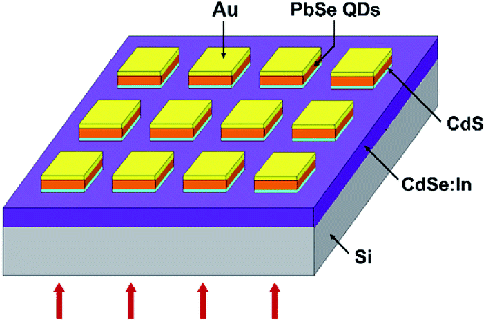 | ||
| Fig. 1 Structural scheme for a PbSe-QDs/CdS/CdSe:In/Si heterojunction photodiode. | ||
2.1 Materials growth
CdSe:In infrared transparent conductive films were synthesized on cleaned Si substrates by co-evaporation of CdSe, indium and selenium in an ultrahigh vacuum thermal evaporation chamber at 2 × 10⁻⁶ Pa. The CdSe:In films of 1.2 μm thicknesses were deposited at 623 K substrate temperature with a constant In/CdSe flux ratio of 0.6% by maintaining temperatures of respective cells at 1143 K and 883 K for 1.5 hours respectively.CdS films were grown on CdSe:In covered Si substrates by chemical bath deposition (CBD). An aqueous precursor was prepared by mixing 8 mM cadmium acetate (Cd(CH3CO2)2), 8 mM ammonium acetate (NH4CH3CO2), 12 mM thiourea (CH4N2S), and 2 M ammonium hydroxide (NH3 H2O, 28%). The CdSe:In/Si substrates were immersed into the precursor with the CdSe:In surfaces facing down. The solution was then heated up and stabilized in a 353 K water bath for 1 h to obtain 300 nm thickness.
PbSe QD films were deposited from the precursor mixed with 3.0 M sodium hydroxide (NaOH), 0.25 M lead acetate (Pb(C2H3O2)2) and 0.25 M selenosulfate (Na2SeSO3) with a concentration ratio of 12![[thin space (1/6-em)]](https://www.rsc.org/images/entities/char_2009.gif) :1:1. Then, the CdS/CdSe:In/Si substrates and glass substrates (as reference) were placed with the CdS surfaces facing down in the solution, mounted on a custom-designed Teflon stage at an angle of 70° with respect to the surface. The growth was carried out at 276 K for 240 h for 1.2 μm thickness.
:1:1. Then, the CdS/CdSe:In/Si substrates and glass substrates (as reference) were placed with the CdS surfaces facing down in the solution, mounted on a custom-designed Teflon stage at an angle of 70° with respect to the surface. The growth was carried out at 276 K for 240 h for 1.2 μm thickness.
2.2 Heterojunction photodiode fabrication
A photoresist (AZ5241E) layer was coated onto the PbSe-QDs/CdS/CdSe:In/Si film by spin-coating at 2500 rpm for 60 s followed by a soft bake at 368 K for 90 s. Then, a quadrate photoresist array with 200 × 200 μm was patterned by using the MJB3 mask aligner UV lithography (275 W) with an exposure time of 10 s, followed by a development time of 45 s. Subsequently, the PbSe QDs/CdS array on CdSe:In layer was obtained by a wet-chemical etching and acetone lift-off. The etchant consists of equal parts of 80% H3PO4, 29% HCI, and H2O. The array was then treated by a post-annealing at 473, 573 and 673 K in air for 0.5 h, accompanied by the PbSe QDs grown on the glass substrates. The electrode pattern was then shaped by a second lithographic process, with a spin-coating at 2500 rpm for 60 s, a soft bake at 368 K for 90 s, an exposure for 4 s, a hard bake at 398 K for 90 s, UV exposure for 50 s and a development for 60 s. Then, a thick 100 nm Au electrode was deposited by thermal evaporation at room temperature for 20 min in 2 × 10⁻⁴ Pa. It should be noted that a 20 nm indium film was deposited over CdSe:In prior to Au deposition for an ohmic contact. Finally, a set of photodiodes with Au/PbSe-QDs/CdS/CdSe:In/Si structures were fabricated after lift-off with acetone for 300 s.2.3 Structure and morphology, optoelectronic and device characterizations
The morphologies of the synthesized thin films were characterized by a Zeiss Neon-40 EsB high-resolution field-emission scanning electron microscope (FESEM). The size and size distribution were calculated from the FESEM image by using the Nanomeasurer 1.2 software. Hall effect measurement was conducted in van der Pauw four-point probe configuration, using fresh indium contacts, in an automated EGK HEM-2000, with a magnetic induction of 0.37 T. For the MWIR PL measurement, PbSe samples were optically pumped by a Q-switched Nd:YAG pulse laser of 1064 nm wavelength. The input power was tuned and calibrated to be at 10 mW on average. The excited spontaneous photon emission from the samples were then collected by a parabolic mirror and redirected into a Bruker IFS-66v Fourier transform infrared spectroscopy. A cryogenic-cooled InSb detector was then used to detect and resolve the frequency dependent signal information. The transmission spectra of the samples were measured by the FTIR system with Si detector from 350–1500 nm, and deuterated triglycine sulfate (DTGS) detector from 1–10 μm. The dark current density–voltage (J–V) behaviour was measured at room temperature by applying bias from −1 to 1 V (Keithley 2400 source meter).The detector performance at room temperature was evaluated by a home-made detectivity measurement system, consisting of an IR-508/301 blackbody (Infrared System Development), an IR-762 modulator (Infrared System Development), a SR830 Lock-in amplifier (Stanford Research System) and a ST-500 probe station (Janis Research). The blackbody temperature was set at 500 K during the measurement, with an integrated radiation intensity of ∼0.355 W cm−2. A mechanical chopper was used to modulate the input signal at a frequency of 750 Hz to avoid environmental and frequency-dependent noises. SR830 lock-in amplifier was used to collect the current signal produced by the detector under zero-bias photovoltaic mode.
Temperature-dependent MWIR spectrum-resolved photoresponses were measured by Bruker IFS-66v Fourier Transform Infrared Spectroscope system. The PbSe-QDs/CdS heterojunction detector was mounted in a Janis VPF-100 vacuum liquid nitrogen cryostat during measurement in the range from 298 K to 160 K.
3 Results and discussion
The as-grown CBD ligand-free PbSe-QDs film synthesized at 276 K appears to be highly adhesive, light-brown in color, smooth surface, uniform and reflecting. The side-view FESEM image of the as-grown film shown in Fig. 2(a) reveals that a uniform, crack-free, glassy close-packed PbSe-QDs film with 1.2 μm thickness, was obtained at a 5 nm h−1 growth rate. The film is made up of the accumulation of individual spherical dots of 6–7 nm in diameter without any voids, and the dot size is constant throughout the thickness of the film. With increasing post-annealing temperatures, the color of PbSe-QDs films gradually deepen to brown, then brownish-black, and finally to grey. At the same time, the transparency quickly declines at annealing temperatures higher than 473 K. Top- and side-view FESEM images shown in Fig. 2(b)–(g) display the morphological evolution of ligand-free PbSe-QDs films with increasing annealing temperatures. Based on the size and distribution calculated from the Nanomeasurer 1.2 software, it is clear the QDs size continuously increases from 6 ± 1 nm to 12 ± 5 nm, 17 ± 4 nm and 25 ± 2 nm, respectively, and the size distribution becomes narrow, as shown in Fig. 2(b)–(d). Meanwhile, PbSe-QDs begin forming multi-QDs aggregates with increasing annealing temperature, resulting in an increased surface roughness. Furthermore, the boundaries of the multi-QDs aggregates become more obvious with the increase of annealing temperature, and eventually develop into micro-cracks (Fig. 2(d) and (g)) when the annealing temperature reaches 673 K. Annealing temperatures beyond 673 K result in increased micro-crack formation, introducing a large number of defect states and negatively impacting device performance. For this reason, 673 K was found to be the upper limit of suitable annealing conditions for our samples. Additionally, a slight increase in thickness with increasing temperature is observed from side-view images.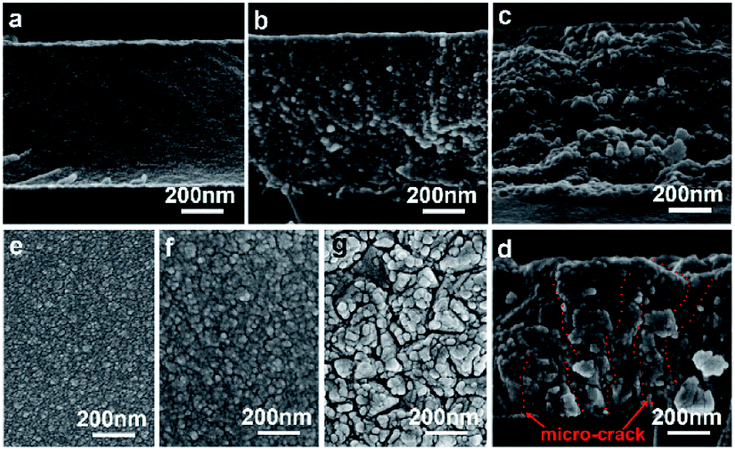 | ||
| Fig. 2 Top- and cross-side view FESEM images of (a) as-grown, (b) and (e) 473 K, (c) and (f) 573 K, (d) and (g) 673 K annealed ligand-free PbSe-QDs synthesized from low-temperature CBD method on glass substrates. Red dotted lines indicate micro-cracks. | ||
During annealing, besides evaporation of excess Se atoms (Se-rich, p-type), heat activates Pb and Se atomic migration by providing enough energy to break Pb–Se bonds, subsequently resulting in grain growth and recrystallization.37–39 As a thermodynamic spontaneous process, the grain growth occurs to reduce the total Gibbs free energy. Due to being ligand-free, the oriented attachment (OA) mechanism dominates the grain growth at relatively low annealing temperature, where adjacent small QDs with common crystallographic orientations combine to form larger ones.37,38 With increasing temperature, Ostwald ripening (OR) becomes the significant grain growth pathway, in which larger QDs are formed by an interface-reaction-limited mass transfer from smaller particles.39 It is the mixed (OA + OR) that results in the increased QDs size, the narrow size distribution, micro-crack formation and coarsening effect.
In addition, thinner surface passivation layers readily form in an oxygen-rich annealing environment due to the diffused oxygen atom's affinity for occupying Se vacancies  40 Oxygen atoms may also react with Pb to form PbO or PbSeO3, especially at high annealing temperatures.41 A recent study has also found the formation of ternary PbOxSe1−x structure, which may form as a result of oxygen atom incorporation.42 This surface oxygen passivation, which is always employed to enhance the photoresponsivity of lead-salt detectors,43 is another reason for the coarsening of the film's surface when annealed at 673 K.
Room temperature photoluminescence (PL) spectra for PbSe-QD films annealed at various temperatures were shown in Fig. 3. No PL emission was detected for the as-grown film along with films annealed at temperatures lower than 373 K, indicating poor QD crystallinity. Poor crystallinity is the result of high defect densities and dislocations introduced by defects, especially concerning selenium interstitials  and lead vacancies
  These defects will act as the radiative recombination centers, quenching the PL emission. After annealing, PL emission is clearly observed from every QDs film annealed at high temperature, indicating that the heat treatment could significantly eliminate the density of intrinsic defects and dislocations by heat-driven atom diffusion (recrystallization and grain growth), improving the PbSe-QDs' crystallinities. With increasing annealing temperature, the PL emission shows an obvious red-shift from 3.2, to 3.5 and 3.70 μm, respectively. It is well known that this red-shift results from the increased QDs size with increasing annealing temperature. The observed size from FESEM images are consistent with Hollingsworth's experimental result,9 in which the QD size corresponding to PL emission peak at 3.2, 3.5 and 3.7 μm should be around 12 ± 0.9 nm, 17 ± 1.9 nm and 23 ± 3 nm, respectively. The sizes generally agree with the corresponding sizes of our annealed PbSe QDs observed from FESEM images.
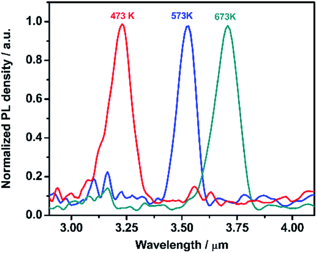 | ||
| Fig. 3 Room temperature PL spectra of PbSe-QDs synthesized from CBD method annealed at different temperatures. | ||
The PbSe-QDs films proved to be p-type conductors by Hall measurement. The as-grown PbSe QD film's Hall mobility is 0.03 cm2 V−1 s−1, which is nearly the same as that of hydrothermal colloidal PbSe QD films with 6–8 nm from spin-coating method. As the annealing temperature increases, the carrier concentration doesn't alter dramatically. However, the mobility shows a rapid increase with annealing temperature, especially at temperatures ranging from 473 to 573 K, as showing in Fig. 4.
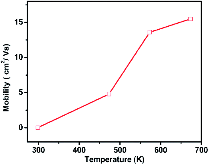 | ||
| Fig. 4 Mobility of PbSe QDs annealed at different temperatures. | ||
The carrier mobility has the following relation:44
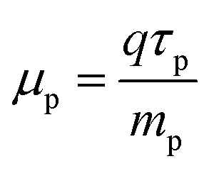
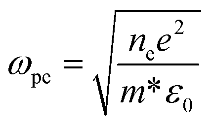
Fig. 5 shows the transmittance spectrum of CdSe:In film deposited on double side polished (DSP, 380 μm) Si substrate using a co-vapour deposition method. Deposition parameters, such as indium concentration and substrate temperature, are optimized to obtain the maximum conductivity as well as keep high transparency in the broad infrared region (1–10 μm). After optimizing In/CdSe beam flux (0.6%), the minimum sheet resistance 40 Ω sq−1 is achieved with an electron density of 7.6 × 1018 cm−3 and a mobility of 204 cm2 V−1 s−1. The average transmittance of the film is 57% in the MWIR (3.0–5.0 μm) region, and more than 40% in the long-infrared (8–10 μm), as shown in Fig. 5. The 57% transmittance of CdSe:In is approximately equal to that of DSP Si substrate at the MWIR range, indicating a coupling of high infrared transparency and high conductivity simultaneously. A lower sheet resistance could be achieved by further increasing the carrier concentration to 5 × 1019 cm−3 through increasing the In/CdSe beam flux ratio. However, higher electron concentrations result in higher plasma frequencies,36 limiting the optical transparency of incident light in the MWIR range. The dependency of plasma frequency on carrier concentration is provided by the following equation:45
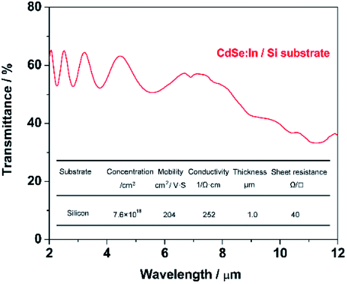 | ||
| Fig. 5 Transmittance of CdSe:In on Si substrate synthesized from co-deposition method. | ||
The dark current density–voltage (J–V) curves of the PbSe-QDs/CdS photodiodes were measured, and shown in Fig. 6. No major changes were observed in the reverse current density and rectifying ratio until annealing temperature reached 673 K. With increasing the annealing temperature to 673 K, the dark current at −0.3 V decreases 3 orders of magnitude from 6–8 mA cm−2 to 3.5 × 10⁻³ mA cm−2, resulting in a more than 144-fold increase in the rectifying ratio measured at ±0.3 V from 1.5 (≤575 K) to 217.
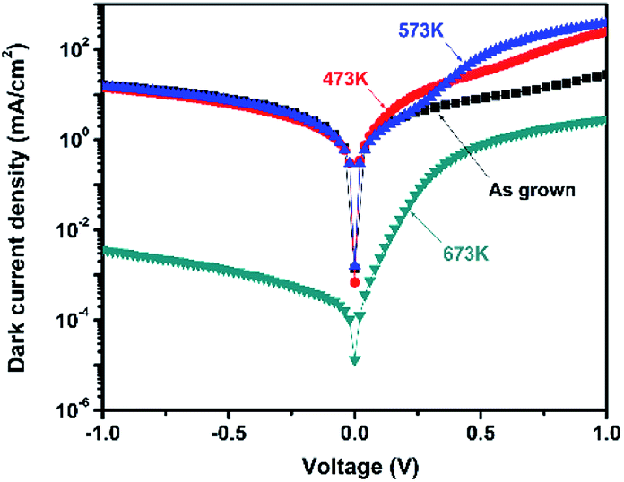 | ||
| Fig. 6 Dark current density–voltage (J–V) characteristics of PbSe-QDs/CdS/CdSe:In/Si photodiodes annealed at various temperatures. | ||
The forward J–V characteristic of a p–n junction can be described by the exponential relation:46
| J ∝ exp(qV/ηTKb) |
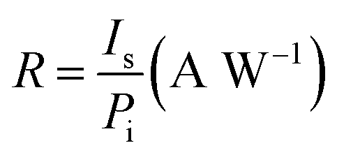
The responsivity R and specific detectivity D* were obtained as described in ref. 48 by using the definition as shown below:40
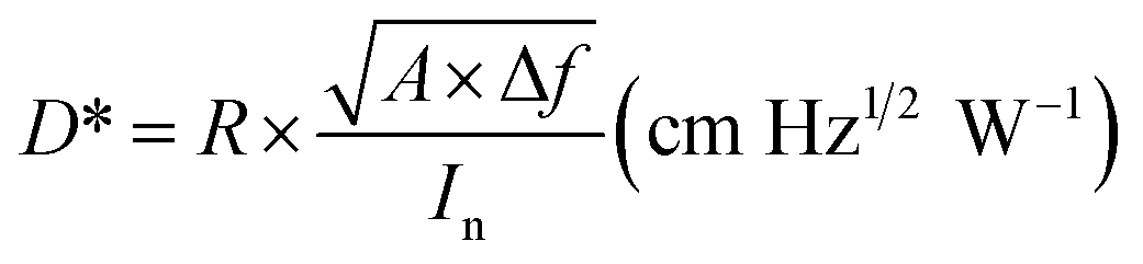
where Is and In are the measured detector output signal and noise currents, A is the device detection area, Δf is the noise bandwidth, and Pi is the incident radiant power. Peak responsivity R and detectivity D* were then calculated through a conversion factor defined in ref. 49.
Under 750 Hz chopping frequency modulation, the detector assembled with PbSe-QDs annealed at 673 K demonstrated the best Rpeak of 0.36 ± 0.04 A W−1 and peak D* of (8.5 ± 1) × 108 cm Hz1/2 W−1 at a cutoff wavelength of 4.2 μm at room temperature based on 57% MWIR transmittance, which is more than one order of magnitude larger than that of devices constructed by low-temperature annealed PbSe-QDs at their corresponding cutoff wavelengths. Measured results from the spectral response shown in Fig. 7 provides an illustration of this comparison.
 | ||
| Fig. 7 Room-temperature spectral response curves of the PbSe-QDs/CdS/CdSe:In/Si photovoltaics annealed at various temperatures. | ||
Fig. 7 shows the spectral response curves for PbSe-QDs/CdS photodiodes annealed at various temperatures. It is clear that spectral response peak and cutoff wavelength move gradually to longer wavelength with increasing annealing temperature, and photoresponse intensity dramatically enhances after annealing temperature reaches 673 K. Only a sharp spectral response peak centered at 650 nm is observed from the photodiode without annealing, implying its potential application in QDs solar cells. As annealing at a lower temperature (≤573 K), the spectral response curve is composed of a sharp and broad band, covering a range from 1 to 2.5 μm (NIR) and 2.5 to 4.5 (MWIR) μm, respectively. This characteristic with obvious divisibility represents two kinds of QDs sizes in low-temperature annealed PbSe-QDs layers. Furthermore, the response peak at the NIR range dramatically decreases with increasing temperature and vanishes as the temperature reaches 673 K, suggesting that higher temperature annealing (≥673 K) is helpful to form larger PbSe-QDs with a uniform size distribution. At the same time, the spectral response peak at the MWIR range is in close agreement with the corresponding PL emission peak, indicating that the red-shift in spectra response curve is a result of the increased size. These results coincide with the results observed from FESEM images and PL spectra. Noticeably, the spectra response center of 3.5 μm and the cutoff of 4.2 μm of CBD PbSe/CdS are smaller than that of single-crystal bulk PbSe/CdS photodiode fabricate by MBE method,50 indicating the MWIR quantum dot photodiode was obtained even after annealing at 673 K.
It should be noted that there is a discrepancy between PL peak (3.75 μm) and the detection cut-off (4.2 μm) for the same sample annealed at 673 K. This discrepancy was always observed from CBD-photoconductive PbSe detectors fabricated in our group,50 which is attributed to the Moss–Burstein shift effect.51 The carrier concentration level of the prepared thin films is below 1019 cm−3, which means they are all mild-doped semiconductor films whose Fermi level lies between the conduction and valence bands. Therefore, with no extra excitation, the measured absorption edge reflects the true energy band gap of the material. However, in terms of the photoluminescence which was measured under the high power pulsed pumping Nd-YAG laser, it will cause significant increase of the electron concentration in the conduction band under the high-energy pulse pumping. This temporal increase of electrons within the conduction band pushes the Fermi level to higher energy which may lie inside the conduction band. In this case, electrons from the top of the valence band can only be excited into the conduction band states higher than the Fermi level since all the states below the Fermi level are occupied states. Considering the parabolic distribution of density of states in the conduction band, most of those excited electrons stay in the states level higher than the conduction band edge. Thus, in the PL measurement, we observed a blue-shift in the peak position compared with the absorption edge measured under the normal FTIR transmission setup.
Although the performance of CdS/PbSe photovoltaic detectors is now 10–30 times lower than the performance (typical 1 × 1010 cm Hz1/2 W−1) of our reported PbSe photoconductors (PC),43 there is a strong market demand for uncooled MIR photovoltaic (PV) detectors because cameras built with a photodiode structure are cheaper, faster, smaller, and lower-power compared to photoconductive cameras. First, photovoltaic CdS/PbSe structure can monolithically integrate on commercially available readout integrated circuit (ROIC), reducing the fabrication cost. Second, the electrode layout at photovoltaic detectors can significantly decrease the pixel size and pitch, achieving a high fill factor and a high resolution. Third, photovoltaic detectors need smaller offset voltage in comparison with its PC counterpart, reducing the weight and power. Since its performance is far below the theoretical limit of Auger recombination,52 there is large room to improve the performance of CdS/PbSe photovoltaic detectors.
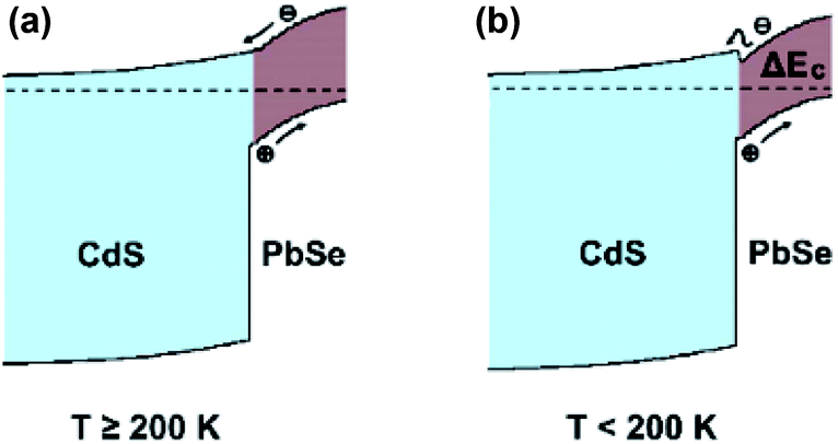
Fig. 8 presents temperature-dependent responsivity of the photodiode with PbSe-QDs annealed at 673 K. As shown in Fig. 8, the cutoff wavelength increases at lower temperatures, however, the responsivity intensity starts to drop below 200 K. This same phenomenon was observed in our previous work about MBE-PbSe/CdS MWIR photovoltaic detector.50
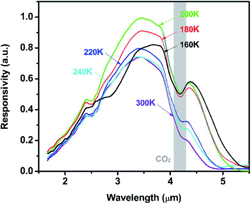 | ||
| Fig. 8 Temperature dependent responsivity of the PbSe-QDs/CdS/CdSe:In/Si photovoltaics annealed at 673 K. | ||
Our previous experiment suggested that the two materials of bulk PbSe and CdS could create a type II band alignment heterojunction at room temperature. The band gap energy (Eg) increases with reducing the size based on the Brus equation shown as follows53
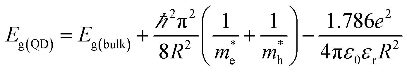
 and
and  are the effective masses of electrons and holes, ε0 and εr are permittivity of vacuum and relative permittivity.
Subsequently, PbSe-QDs have higher LUMO compared with the bottom of the conduction band for bulk PbSe. The alignment of PbSe-QDs/CdS p–n junction must be type II as shown in Fig. 9, so that the photo-excited electrons generated in PbSe-QDs can efficiently inject into CdS film. It is well known that the photo-generated carriers in PbSe films, especially at lower temperatures, is dominated by the diffusion length and absorption coefficient.41 Since both the diffusion length and absorption coefficient increase with decreasing temperature based on the multiband-model theory, lowing temperature increase the generated carrier density, leading to an enhanced photoresponse intensity.
 | ||
| Fig. 9 Band diagram of the 673 K annealed PbSe-QDs/CdS heterojunction at (a) above 200 K and (b) below 200 K. | ||
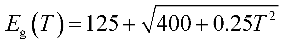
At the same time, as a material with a positive temperature coefficient, the band gap of PbSe QDs (≥5 nm) reduces with falling temperature, which can be approximated by Preier's expression:54
This causes a redshift in cutoff wavelength at low temperatures. This is also proved by a steady red shift of cutoff wavelength from 4.2 to 4.75 μm with the temperature dropping from 300 to 160 K. However, CdS has a negative temperature coefficient which can be expressed by:55
| Eg(T) = 2.5825 − 3.06 × 10⁻³ × T2/(2156 + T) |
Therefore, we suggest that the opposite temperature coefficient between PbSe and CdS triggers the band alignment transformation from type-II to type-I as temperature low than 200 K, as shown in Fig. 9.
Consequently, the barrier introduced by the change of conduction band offset could gradually hinder the diffusion of photo-generated electrons by a factor of 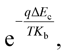 which is larger than the increased intensity resulting from the increase of Le at lower temperature. This would result in photoresponse intensity dropping as temperature reaches below 200 K.
4 Conclusions
In summary, we've demonstrated a new all-solution synthetic procedure to assemble low-cost, uncooled PbSe-QDs/CdS p–n heterojunction photodiodes. A series of annealing-temperature control experiments suggest the photoresponse wavelength of the ligand-free QDs photodiodes could be tailored from visible to MWIR with increasing temperature. The photoresponse redshift is attributed to the increased QDs size, resulting from grain growth and recrystallization triggered by high temperature. At the same time, higher annealing temperature is helpful to enhance the performance of photodiodes by improving the QDs crystallinity and decreasing the interface defect density between PbSe-QDs and CdS, which can significantly supress the dark current and improve the photocurrent. The maximum peak responsivity Rpeak of 0.36 ± 0.04 A W−1 and specific detectivity D* of (8.5 ± 1) × 108 cm Hz1/2 W−1 with a cutoff wavelength of 4.2 μm were achieved after annealing at 673 K for 0.5 h. In addition, an abnormal performance decrease was observed when the measurement temperature is lower than 200 K, which may be caused by a band alignment transition from type-II to type-I, as a result of a reverse temperature coefficients of the two materials. It is believed that the performance could be significantly improved through future optimizations in both structure design and material quality improvement. Furthermore, CdSe:In films fabricated by co-vapor deposition proved promising as a high infrared transparent conductive electrode, paving the way for furthering structural design diversity of next-generation MIR photodiodes.Conflicts of interest
There are no conflicts to declare.Acknowledgements
This work is partially supported by the US DARPA STTR, army research office (ARO) and Oklahoma Center for the Advancement of Science and Technology (OCAST) under contract/Grant No. D14PC00021, W911NF-14-1-0312, and AR132-003.Notes and references
- S. A. McDonald, G. Konstantatos, S. Zhang, P. W. Cyr, E. J. Klem, L. Levina and E. H. Sargent, Nat. Mater., 2005, 4, 138–142 CrossRef CAS PubMed.
- K. S. Jeong, J. Tang, H. Liu, J. Kim, A. W. Schaefer, K. Kemp, L. Levina, X. Wang, S. Hoogland, R. Debnath, L. Brzozowski, E. H. Sargent and J. B. Asbury, ACS Nano, 2012, 6, 89–99 CrossRef CAS PubMed.
- J. Zhang, J. Gao, C. P. Church, E. M. Miller, J. M. Luther, V. I. Klimov and M. C. Beard, Nano Lett., 2014, 14, 6010–6015 CrossRef CAS PubMed.
- G. Konstantatos and E. H. Sargent, Proc. IEEE, 2009, 97, 1666–1683 CAS.
- J. J. Urban, D. V. Talapin, E. V. Shevchenko and C. B. Murray, J. Am. Chem. Soc., 2006, 128, 3248–3255 CrossRef CAS PubMed.
- B. N. Pal, I. Robel, A. Mohite, R. Laocharoensuk, D. J. Werder and I. Klimov, Adv. Funct. Mater., 2012, 22, 1741–1748 CrossRef CAS.
- I. Kang and F. W. Wise, J. Opt. Soc. Am. B, 1997, 14, 1632–1646 CrossRef CAS.
- I. Moreels, K. Lambert, D. Smeets, D. De Muynck, T. Nollet, J. C. Martins, F. Vanhaecke, A. Vantomme, C. Delerue, G. Allan and Z. Hens, ACS Nano, 2009, 3, 3023–3030 CrossRef CAS PubMed.
- J. M. Pietryga, R. D. Schaller, D. Werder, M. H. Stewart, V. I. Klimov and J. A. Hollingsworth, J. Am. Chem. Soc., 2004, 126, 11752–11753 CrossRef CAS PubMed.
- V. Sukhovatkin, S. Hinds, L. Brzozowski and E. H. Sargent, Science, 2009, 324, 1542–1544 CrossRef CAS PubMed.
- J. Gao, A. F. Fidler and V. I. Klimov, Nat. Commun., 2015, 6, 8185 CrossRef PubMed.
- Y. Wang, X. Bai, T. Wang, L. Yan, T. Zhang, Y. Zhang and W. W. Yu, Nanotechnology, 2017, 28, 215703 CrossRef PubMed.
- W. Hu, R. Henderson, Y. Zhang, G. You, L. Wei, Y. Bai, J. Wang and J. Xu, Nanotechnology, 2012, 23, 375202 CrossRef PubMed.
- K. S. Leschkies, T. J. Beatty, M. S. Kang, D. J. Norris and E. S. Aydi, ACS Nano, 2009, 3, 3638–3648 CrossRef CAS PubMed.
- X. Zhang, Y. Zhang, L. Yan, C. Ji, H. Wu, Y. Wang, P. Wang, T. Zhang, Y. Wang, T. Cui, J. Zhao and W. W. Yu, J. Mater. Chem. A, 2015, 3, 8501–8507 RSC.
- A. Munoz, J. Melendez, M. C. Torquemada, M. T. Rodrigo, J. Cebrian, A. J. de Castro, J. Meneses, M. Ugarte, F. Lopez, G. Vergara, J. L. Hernandez, J. M. Martın, L. Adell and M. T. Montojo, Thin Solid Films, 1998, 317, 425–428 CrossRef CAS.
- T. Zhu, L. Zheng, X. Yao, L. Liu, F. Huang, Y. Cao and X. Gong, ACS Appl. Mater. Interfaces, 2019, 11(9), 9205–9212 CrossRef CAS PubMed.
- X. Xing, Y. Lei, W. Shang, L. Du and P. Guo, J. Nanomater., 2017, 2017, 1–5 CrossRef.
- L. Yan, Y. Zhang, T. Zhang, Y. Feng, K. Zhu, D. Wang, T. Cui, J. Yin, Y. Wang, J. Zhao, W. W. Yu and Y. Long, Anal. Chem., 2014, 86, 11312–11318 CrossRef CAS PubMed.
- S. Baskoutas and A. F. Terzis, J. Appl. Phys., 2006, 99, 013708 CrossRef.
- C. Wang, G. Zhang, S. Fan and Y. Li, J. Phys. Chem. Solids, 2001, 62, 1957–1960 CrossRef CAS.
- E. Lifshitz, M. Brumer, A. Kigel, A. Sashchiuk, M. Bashouti, M. Sirota, E. Galun, Z. Burshtein, A. Q. Le Quang, I. Ledoux-Rak and J. Zys, J. Phys. Chem. B, 2006, 110, 25356–25365 CrossRef CAS PubMed.
- J. H. Warner, Adv. Mater., 2008, 20, 784–787 CrossRef CAS.
- J. Qiu, B. Weng, W. Ge, L. L McDowell, Z. Cai and Z. Shi, Sol. Energy Mater. Sol. Cells, 2017, 172, 117–123 CrossRef CAS.
- C. R. Pidgeon, C. M. Ciesla and B. N. Murdin, Prog. Quantum Electron., 1998, 21, 361–419 CrossRef.
- M. Sulaman, S. Yang, A. Bukhtiar, C. Fu, T. Song, H. i. Wang, Y. Wang, H. Bo, Y. Tang and B. Zou, RSC Adv., 2016, 6, 44514–44521 RSC.
- M. Thambidurai, Y. Jang, A. Shapiro, G. Yuan, H. Xiaonan, Y. Xuechao, Q. J. Wang, E. Lifshitz, H. V. Demir and C. Dang, Opt. Mater. Express, 2017, 7, 2326–2335 CrossRef CAS.
- G. H. Carey, A. L. Abdelhady, Z. Ning, S. M. Thon, O. M. Bakr and E. H. Sargent, Chem. Rev., 2015, 115, 12732–12763 CrossRef CAS PubMed.
- D. Zhitomirsky, O. Voznyy, L. Levina, S. Hoogland, K. W. Kemp, A. H. Ip, S. M. Thon and E. H. Sargent, Nat. Commun., 2014, 5, 3803 CrossRef CAS PubMed.
- I. Hamberg and C. G. Granqvist, Appl. Opt., 1985, 24, 1815–1819 CrossRef CAS PubMed.
- Z. Wu, Z. Chen, X. Du, J. M. Logan, J. Sippel, M. Nikolou, K. Kamaras, J. R. Reynolds, D. B. Tanner, A. F. Hebard and A. G. Rinzler, Science, 2004, 305, 1273–1276 CrossRef CAS PubMed.
- E. Sachet, C. T. Shelton, J. S. Harris, B. E. Gaddy, D. L. Irving, S. Curtarolo, B. F. Donovan, P. E. Hopkins, P. A. Sharma, A. Lima Sharma, J. Ihlefeld, S. Franzen and J. P. Maria, Nat. Mater., 2015, 14, 414–420 CrossRef CAS PubMed.
- D. S. Ghosh, L. Martinez, S. Giurgola, P. Vergani and V. Pruneri, Opt. Lett., 2009, 34, 325–327 CrossRef CAS PubMed.
- A. Stadler, Materials, 2012, 5, 661–683 CrossRef PubMed.
- Y. Chuai, X. Wang, C. Zheng, Y. Zhang, H. Shen and Y. Wang, RSC Adv., 2016, 6, 31726–31731 RSC.
- R. K. Swank, Phys. Rev., 1967, 153, 844–849 CrossRef CAS.
- E. J. H. Lee, C. Ribeiro, E. Longo and E. R. Leite, J. Phys. Chem. B, 2005, 109, 20842–20846 CrossRef CAS PubMed.
- J. Zhang, F. Huang and Z. Lin, Nanoscale, 2010, 2, 18–34 RSC.
- N. T. K. Thanh, N. Maclean and S. Mahiddine, Chem. Rev., 2014, 114, 7610–7630 CrossRef CAS PubMed.
- F. Zhao, S. Mukherjee, J. Ma, D. Li, S. L. Elizondo and Z. Shi, Appl. Phys. Lett., 2008, 92, 211110 CrossRef.
- W.-F. Li, C.- M Famg, M. Dijkstra and M. A van Huis, J. Phys.: Condens. Matter, 2015, 27, 355801 CrossRef PubMed.
- L. McDowell, J. Qiu, B. Weng and Z. Shi, Cryst. Growth Des., 2019, 19, 2253–2258 CrossRef CAS.
- J. Qiu, B. Weng, Z. Yuan and Z. Shi, J. Appl. Phys., 2013, 113, 103102 CrossRef.
- C. C. Hu, Modern Semiconductor Devices for Integrated Circuits, Pearson, 2009, ch. 2, p. 38 Search PubMed.
- R. C. Jayasinghe, Y. F. Lao, A. G. U. Perera, M. Hammar, C. F. Cao and H. Z. Wu, J. Phys.: Condens. Matter, 2012, 24, 435803 CrossRef CAS PubMed.
- A. Rogalski, Infrared detectors, Taylor and Francis Group, LLC and. CRC Press, 2nd edn, 2011 Search PubMed.
- C. Sah, R. N. Noyce and W. Shockley, Proc. IRE, 1957, 45, 1228–1243 Search PubMed.
- B. Weng, J. Qiu, L. Zhao, C. Chang and Z. Shi, Appl. Phys. Lett., 2014, 104, 121111 CrossRef.
- E. L. Dereniak and G. D. Boreman, Infrared Detectors and Systems, John Wiley & Sons, New York, 1996, p. 208 Search PubMed.
- B. Weng, J. Qiu, Z. Yuan, P. Larson and Z. Shi, Appl. Phys. Lett., 2014, 104, 021109 CrossRef.
- E. D. Palik, D. L. Mitchell and J. N. Zemel, Phys. Rev., 1964, 135, 763–778 CrossRef.
- X. Shi, Q. Phan, B. Weng, L. McDowell, J. Qiu, Z. Cai and Z. Shi, Detection, 2018, 6, 1–16 CrossRef CAS.
- E. O. Chukwuocha, M. C. Onyeaju and T. S. T. Harry, World J. Condens. Matter Phys., 2012, 2, 96–100 CrossRef CAS.
- E. Pedrueza, A. Segura, R. Abargues, J. B. Bailach, J. Claude Chervin and J. P. Martınez-Pastor, Nanotechnology, 2013, 24, 205701 CrossRef PubMed.
- Y. P. Varshni, Physica, 1967, 34, 149–154 CrossRef CAS.
Footnote |
| † Jijun Qiu and Binbin Weng contributed equally to this work. |
| This journal is © The Royal Society of Chemistry 2019 |