
 Open Access Article
 This Open Access Article is licensed under a Creative Commons Attribution-Non Commercial 3.0 Unported Licence
Patterned films of a hybrid lead halide perovskite grown using space-confined conversion of metallic lead by reactive polyiodide melts
Aleksei Y. Grishkoa,
Andrey A. Petrov a,
Eugene A. Goodilinabc and
Alexey B. Tarasov*ab
a,
Eugene A. Goodilinabc and
Alexey B. Tarasov*ab
aLaboratory of New Materials for Solar Energetics, Department of Materials Science, Lomonosov Moscow State University, Lenin Hills, 119991 Moscow, Russia. E-mail: alexey.bor.tarasov@yandex.ru
bDepartment of Chemistry, Lomonosov Moscow State University, 1 Lenin Hills, 119991 Moscow, Russia
cKurnakov Institute of General and Inorganic Chemistry, 31 Leninsky Prospekt, 119992, Moscow, Russia
First published on 18th November 2019
Abstract
A unique technique for preparation of thin patterned perovskite films is suggested based on an interaction of reactive polyiodide melts with metallic lead coatings using a patterned die with a given relief. The growth of perovskite in confined space results in pin-hole free textured films.
Perovskite photovoltaics has experienced tremendous growth since 2009, when Miyasaka used MAPbI3 (MA = CH3NH3+) as a sensitizer in a DSSC and obtained the efficiency of 3.6%.1 In less than 10 years, perovskite solar cells have reached the efficiency of 25.2% (ref. 2) and proved to be a competitor to silicon and thin-film solar cells. Texturing of the light-absorbing layer in a solar cell can greatly improve its efficiency due to optimization of light-scattering3 and, in particular increase the efficiency of silicon-perovskite tandems up to 25.5%.4–6 Simulation studies suggest large improvement of the efficiencies for the nanopatterned perovskite films7–10 that was also confirmed experimentally.11
The variety of approaches to obtained patterned films include etching12,13 and micro-structuring14 of the substrate, sacrificial template synthesis, crystallization from the solution under the stamp,15 and direct deformation of perovskite layer by molding.16 While substrate surface modification only allows to texture bottom side of the perovskite film, other approaches result in texturing of the top side of the perovskite film.
Recently, a new precursor with the formula MAIx>3 coined as reactive polyiodide melts (RPM) was discovered which converts metallic lead films into high-quality large-area MAPbI3 films17,18 through a simple reaction: MAI3 + Pb → MAPbI3 without any byproducts. In this report, we realize this reaction under confined space conditions between metallic lead coating and a patterned die thus developing a new method for fabrication of hybrid perovskite thin films with a flexibly controlled surface pattern.
As a key solution, a droplet of RPM was deposited onto a plastic die with a striped relief and squeezed between the die and the thin film of metallic lead to initiate reactive confined growth of a hybrid perovskite layer. In our study we used a commercially available polyethylene terephthalate diffraction grating with 500 nm width and 280 nm depth of the stripes therefore providing the confined volume of 14![[thin space (1/6-em)]](https://www.rsc.org/images/entities/char_2009.gif) 000 μm3 per 1 cm2 of the die. We demonstrate that constraining of the RPM to the free volume between surfaces of the die and the metallic lead film allows to achieve a desired final morphology of the perovskite MAPbI3 film. The control over the shape of the die thus provides a convenient way to fabricate perovskite films with a given relief.
000 μm3 per 1 cm2 of the die. We demonstrate that constraining of the RPM to the free volume between surfaces of the die and the metallic lead film allows to achieve a desired final morphology of the perovskite MAPbI3 film. The control over the shape of the die thus provides a convenient way to fabricate perovskite films with a given relief.
The interplay between absorption and charge collection by the electron- and hole-transporting layers requires the perovskite layer to be 300–800 nm thick9,19 for the maximum performance of the solar cell. The molar volume of hybrid perovskite MAPbI3 is 8.3 times larger than that of metallic lead, therefore 35–100 nm of metallic lead is sufficient to form dense perovskite layer of the desired thickness.
We developed a new approach that allows a precise dosing of RPM that is based on the interaction of RPM with lead. We achieve this by pressing the die with a given relief containing RPM deposited onto it against the metallic lead film as depicted in Fig. 1.
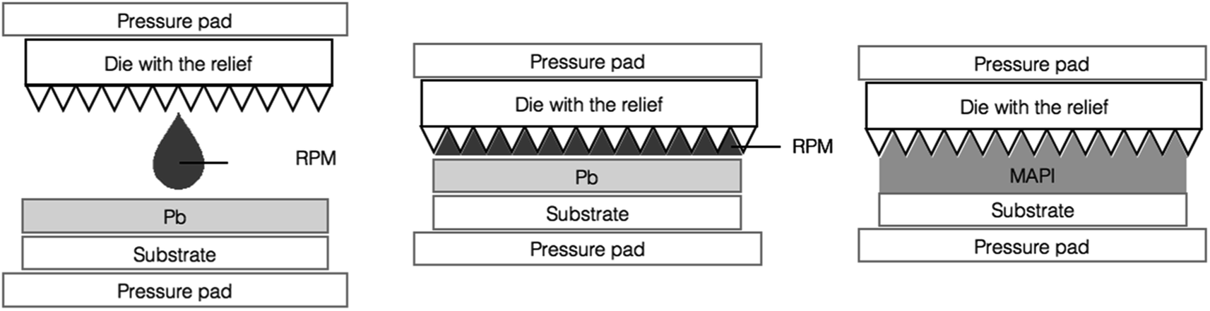 | ||
| Fig. 1 The scheme of the fabrication of the perovskite thin films using the space-confined conversion of metallic lead with RPM. | ||
When a die is brought into physical contact with the metallic lead film, the RPM is immediately distributed over the whole substrate. In this implementation RPM/Pb reagent ratio is determined by the volume of the RPM between the die with a relief and the substrate. Because of the large difference in molar volumes of CH3NH3PbI3 and Pb, the interface between the growing perovskite film and the die develops tangentially to the surface. Once the perovskite crystallization front reaches the surface of the die, its vertical growth gets blocked and the lateral growth starts. This ensures full coverage of the substrate and exact replication of the die relief by the as-formed perovskite film. Moreover, at the stage of lateral growth, the excess of RPM is pushed away from the space between the die and the perovskite film by the growing perovskite grains. By optimizing the exposure time of the metallic lead film to RPM before pressing the die against it, we obtained single-phase perovskite films (Fig. 2d) with a thickness of ∼800 nm. The typical morphology of the perovskite films fabricated under space-confined conditions is shown in Fig. 2a–c. One can see that this film consists of ∼300–1000 nm size perovskite grains which completely cover the substrate. The relief of the perovskite film obtained by this method replicates the die which demonstrates that an arbitrary relief can be transfered to the final perovskite film.
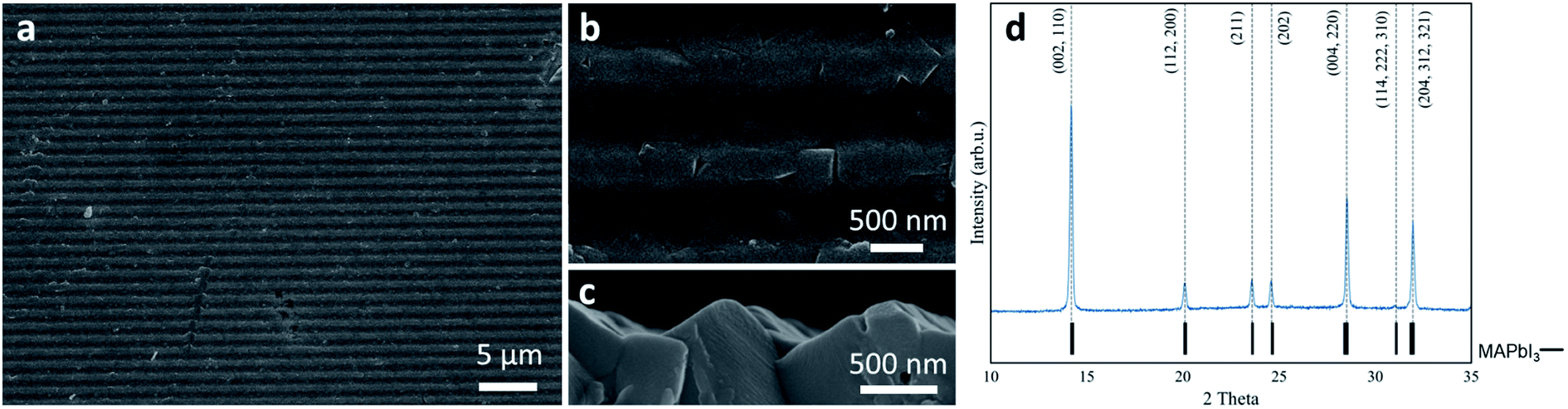 | ||
| Fig. 2 SEM images (a–c) and XRD (d) of the film obtained by space-confined growth method. | ||
Moreover, we discovered that the high concentration of the RPM components and high recrystallization ability of the MAI-I2 system allows modification of the surface relief of the perovskite films obtained by other methods. In order to exemplify this approach, we obtained a perovskite film using conversion of metallic lead by RPM under free growth conditions with consequent rinsing with isopropyl alcohol (Fig. 3a). Then we pressed the die with the relief with a thin layer of RPM on it against the as-prepared perovskite film, waited for 10 minutes, washed an excess of RPM with isopropyl alcohol and disassembled the reaction pair. The morphology of the film adopted the morphology of the die and appeared to be exactly the same as the one obtained using space-confined growth (Fig. 3b).
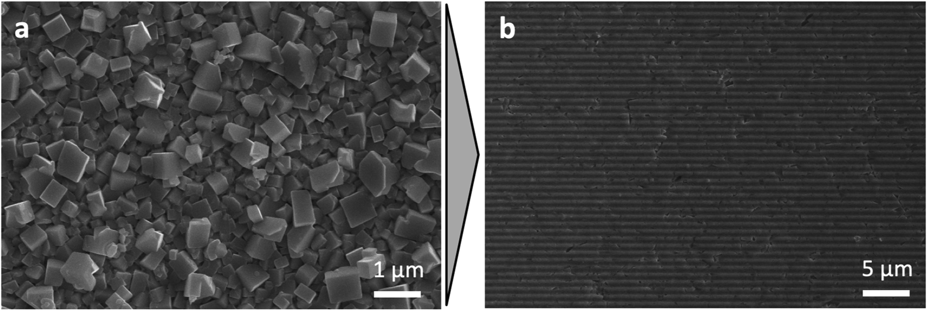 | ||
| Fig. 3 SEM images of the perovskite film before (a) and after (b) recrystallization in the confined space launched by pressing the die with a relief with a thin layer of RPM on it against that film. | ||
Thus, high concentration of the components in the RPM allows for the vertically confined growth and ensures high recrystallization ability of the RPM which make it possible to transfer the relief of the die to the perovskite film. The preparation of a single-phase perovskite in the form of large-crystalline film with a surface relief using the novel confined growth approach makes it possible to scale up the process of solar perovskite production and allows for new techniques that add recently unavailable flexibility to the process of fabrication of solar cells. In addition, further applications of artificial reliefs would allow to develop texturing procedures due to the effect of graphoepitaxy20 and also have a potential of providing higher efficiency of light harvesting by lower reflectivity on patterned light absorbing surfaces.
Experimental part
Thin metallic lead films (35–100 nm) were deposited by means of thermal evaporation in vacuum (10−5 torr). Reactive polyiodide melts were prepared by mixing powders of CH3NH3I and I2 (1:2 mol) at room temperature. In order to convert thin films of metallic lead into perovskite films, a droplet of the as-prepared melt was deposited onto the surface of the die with a striped relief (PET diffraction grating with 1000 lines per cm was used as a die) that was squeezed against thin film of metallic lead. Die was held in contact with the substrate for 5–10 minutes to ensure the complete conversion. Excess of the melt was washed away from the exterior of the reaction cell by excessive amount of isopropyl alcohol.
X-ray powder diffraction data was obtained on Bruker D8 Advance, morphology of thin films was examined by means of Zeiss Supra 40 scanning electron microscope.
Conflicts of interest
There are no conflicts to declare.Acknowledgements
Authors are grateful to the Development Program of Lomonosov Moscow State University.References
- A. Kojima, K. Teshima, Y. Shirai and T. Miyasaka, J. Am. Chem. Soc., 2009, 131, 6050–6051 CrossRef CAS PubMed.
- Best Research-Cell Efficiencies (NREL), accessed Oct 29, 2019.
- K. X. Wang, Z. Yu, V. Liu, Y. Cui and S. Fan, Nano Lett., 2012, 12, 1616–1619 CrossRef CAS PubMed.
- G. Nogay, F. Sahli, J. Werner, R. Monnard, M. Boccard, M. Despeisse, F.-J. Haug, Q. Jeangros, A. Ingenito and C. Ballif, ACS Energy Lett., 2019, 4, 844–845 CrossRef CAS.
- M. Jošt, E. Köhnen, A. B. Morales-Vilches, B. Lipovšek, K. Jäger, B. Macco, A. Al-Ashouri, J. Krč, L. Korte, B. Rech, R. Schlatmann, M. Topič, B. Stannowski and S. Albrecht, Energy Environ. Sci., 2018, 11, 3511–3523 RSC.
- H. Kanda, N. Shibayama, A. Uzum, T. Umeyama, H. Imahori, K. Ibi and S. Ito, ACS Appl. Mater. Interfaces, 2018, 10, 35016–35024 CrossRef CAS PubMed.
- Z. Xie, S. Sun, W. Wang, L. Qin, Y. Yan, R. Hou and G. G. Qin, Opt. Commun., 2018, 410, 117–122 CrossRef CAS.
- J. van Deelen, Y. Tezsevin and M. Barink, MRS Adv., 2017, 2, 3091–3098 CrossRef CAS.
- W. E. I. Sha, X. Ren, L. Chen and W. C. H. Choy, Appl. Phys. Lett., 2015, 106, 221104 CrossRef.
- Z. Xie, S. Sun, X. Xie, R. Hou, W. Xu, Y. Li and G. G. Qin, Semicond. Sci. Technol., 2018, 33, 015011 CrossRef.
- X. Yang, J. Wu, T. Liu and R. Zhu, Small Methods, 2018, 2, 1800110 CrossRef.
- F. Wang, Y. Zhang, M. Yang, L. Fan, L. Yang, Y. Sui, J. Yang and X. Zhang, Nano Energy, 2019, 60, 198–204 CrossRef CAS.
- D. I. Kim, S.-H. Nam, K.-H. Hwang, Y.-M. Lee and J.-H. Boo, Funct. Mater. Lett., 2016, 09, 1642011 CrossRef CAS.
- R. T. Ginting, E.-B. Jeon, J.-M. Kim, W.-Y. Jin and J.-W. Kang, ACS Appl. Mater. Interfaces, 2018, 10, 31291–31299 CrossRef CAS PubMed.
- M. E. Kamminga, H. H. Fang, M. A. Loi, G. H. Ten Brink, G. R. Blake, T. T. M. Palstra and J. E. Ten Elshof, ACS Appl. Mater. Interfaces, 2018, 10, 12878–12885 CrossRef CAS PubMed.
- H. Wang, R. Haroldson, B. Balachandran, A. Zakhidov, S. Sohal, J. Y. Chan, A. Zakhidov and W. Hu, ACS Nano, 2016, 10, 10921–10928 CrossRef CAS PubMed.
- A. A. Petrov, N. A. Belich, A. Y. Grishko, N. M. Stepanov, S. G. Dorofeev, E. G. Maksimov, A. V. Shevelkov, S. M. Zakeeruddin, M. Graetzel, A. B. Tarasov and E. A. Goodilin, Mater. Horiz., 2017, 4, 625–632 RSC.
- I. Turkevych, S. Kazaoui, N. A. Belich, A. Y. Grishko, S. A. Fateev, A. A. Petrov, T. Urano, S. Aramaki, S. Kosar, M. Kondo, E. A. Goodilin, M. Graetzel and A. B. Tarasov, Nat. Nanotechnol., 2019, 14, 57–63 CrossRef CAS PubMed.
- D. Liu, M. K. Gangishetty and T. L. Kelly, J. Mater. Chem. A, 2014, 2, 19873–19881 RSC.
- E. A. Goodilin, E. S. Reddy, J. G. Noudem, M. Tarka and G. J. Schmitz, Phys. C, 2002, 372–376, 842–845 CrossRef CAS.
| This journal is © The Royal Society of Chemistry 2019 |