
 Open Access Article
 This Open Access Article is licensed under a
 Creative Commons Attribution 3.0 Unported Licence
Fluorine ion induced phase evolution of tin-based perovskite thin films: structure and properties†
Junsheng Wu ab,
Fang Fanga,
Zhuo Zhaoab,
Tong Liab,
Rizwan Ullahc,
Zhe Lvb,
Yanwen Zhou*a and
David Sawtell*d
ab,
Fang Fanga,
Zhuo Zhaoab,
Tong Liab,
Rizwan Ullahc,
Zhe Lvb,
Yanwen Zhou*a and
David Sawtell*d
aSchool of Chemical Engineering, University of Science and Technology Liaoning, 114051 Liaoning, Anshan, China
bInstitute of Surface Engineering, University of Science and Technology Liaoning, Anshan, 114051 Liaoning, China. E-mail: zhouyanwen@ustl.edu.cn
cDepartment of Physics, Beijing Normal University, 100875 Beijing, China
dSurface Engineering Group, Manchester Metropolitan University, Manchester M1 5GD, England, UK. E-mail: d.sawtell@mmu.ac.uk
First published on 13th November 2019
Abstract
To study the effect of fluorine ions on the phase transformation of a tin-based perovskite, CsSnI3−x(F)x films were deposited by using thermal vacuum evaporation from a mixed powder of SnI2, SnF2 and CsI, followed by rapid vacuum annealing. The color evolution, structure, and properties of CsSnI3−xFx films aged in air were observed and analyzed. The results showed that the colors of the films changed from black to yellow, and finally presented as black again over time; the unstable B-γ-CsSnI3−xFx phase transformed into the Y-CsSnI3−xFx phase, which is then recombined into the Cs2SnI6−xFx phase with the generation of SnO2 in air. Fluorine dopant inhibited the oxidation process. The postponement of the phase transformation is due to the stronger bonds between F and Sn than that between I and Sn. The color changing process of the CsSnI3−xFx films slowed that the hole concentrations increased and the resistivities decreased with the increase of the F dopant ratio. With the addition of SnF2, light harvesting within the visible light region was significantly enhanced. Comparison of the optical and electrical properties of the fresh annealed CsSnI3−xFx films showed that the band gaps of the aged films widened, the hole concentrations kept the same order, the hole mobilities reduced and therefore, the resistivities increased. The double layer Cs2SnI6−xFx phase also showed ‘p’ type semi-conductor properties, which might be due to the incomplete transition of Sn2+ to Sn4+, i.e. Sn2+ provides holes as the acceptor.
1. Introduction
Within the past decade, inorganic–organic hybrid perovskite solar cells have drawn researchers' attention for their enhanced efficiencies due to their superior long diffusion length, with a conversion efficiency of approximately 3.8% in 2009![[thin space (1/6-em)]](https://www.rsc.org/images/entities/char_2009.gif) 1 to greater than 23.32% today.2 Since the early reports of lead (Pb)3 and tin (Sn)4 based perovskite solar cells, the efficiencies of Pb based perovskite solar cells have increased to nearly 22%, which exceeds those of poly-silicon solar cells.5 Although most studies are focused on MAPbX3 perovskite materials, tin-based perovskite has attracted more and more attention due to the low toxicity of tin.6 So far, the literature7,8 has reported that both Sn doped and the entirely Sn based perovskite solar cells (ASnX3) are not as efficient as Pb-based perovskite solar cells due to two primary reasons: (1) tin is easily oxidized from Sn2+ to Sn4+ oxidation states whilst exposed to air.9,10 The diffusion length of the photogenic carriers is limited because of too many p-type carriers produced by the self-doping effect within the tin-based perovskite materials; (2) SnI2 and MAI (CH3NH3I−) reacts quickly and rapidly crystallizes during spin-coating process9,11 and therefore, it is difficult to control the crystallinity of perovskite, lead to poor coverage and uniformity of the film. To combat this stable and defect free ASnX3films are required.
1 to greater than 23.32% today.2 Since the early reports of lead (Pb)3 and tin (Sn)4 based perovskite solar cells, the efficiencies of Pb based perovskite solar cells have increased to nearly 22%, which exceeds those of poly-silicon solar cells.5 Although most studies are focused on MAPbX3 perovskite materials, tin-based perovskite has attracted more and more attention due to the low toxicity of tin.6 So far, the literature7,8 has reported that both Sn doped and the entirely Sn based perovskite solar cells (ASnX3) are not as efficient as Pb-based perovskite solar cells due to two primary reasons: (1) tin is easily oxidized from Sn2+ to Sn4+ oxidation states whilst exposed to air.9,10 The diffusion length of the photogenic carriers is limited because of too many p-type carriers produced by the self-doping effect within the tin-based perovskite materials; (2) SnI2 and MAI (CH3NH3I−) reacts quickly and rapidly crystallizes during spin-coating process9,11 and therefore, it is difficult to control the crystallinity of perovskite, lead to poor coverage and uniformity of the film. To combat this stable and defect free ASnX3films are required.
Inorganic materials generally have higher stability than organic materials. For this reason, the studies on inorganic perovskite materials have been proposed. As the standard ASnX3 perovskite, the schematic crystal structure of B-γ-CsSnI3, Y-CsSnI3 and Cs2SnI6 are shown in Fig. 1, in which the B-γ-CsSnI3 phase is black with a three dimensional perovskite structure,12 the Y-CsSnI3 phase is yellow with a one-dimensional double-chain structure,13 and Cs2SnI6 is black with double layer perovskite structure. The unstable B-γ-CsSnI3 phase promptly transforms to the Y-CsSnI3 phase, then forms into the Cs2SnI6 phase in air, accompanied with the formation of SnO2. The compound of Cs2SnI6 exhibits its stability in damp air due to the stable Sn4+ state. The ‘vacancy ordered’ double layer perovskite structure is formed by the missing half of the Sn atoms located in the center of octahedral, and then reconstitutes to the discontinuous regular octahedral structure (SnI6).2–14
 | ||
| Fig. 1 Polyhedral model of (a) B-γ-CsSnI3. (b) Y-CsSnI3. (c) Cs2SnI6 and (d) CsSnF3. SnI6 octahedra are in gray, Cs is in green, Sn is in gray, the I anions are purple, and F is blue. | ||
ASnX3 perovskite structure (A = metal or NH4 and X = halogen family) generally consists of (SnX3)− and M+, in which Sn2+ is unstable. Vilminot originally discussed evolution of the ionic-conductivity of the MSnF3 phases (M = Na, K, Rb, Cs, NH4, Tl) in 1985.15 For example, CsSnF3 exhibits a crystal structure consisting of isolated (SnF3)− anionic polyhedral,16 shown in Fig. 1d. Each Sn2+ cation in CsSnF3 is bonded to three fluorine atoms in a distorted triangular pyramidal coordination environment, i.e. the lone pair of 5s electrons of tin(II) and three pairs of electrons, shared unequally with the fluorine ions, occupied on the most stable configuration sp3 hybridization orbits.17
Researchers and experiments have shown that the tolerance factors of the stable perovskite materials should be between 0.78–1.05,18 in which the tolerance factor, t = (RA + RX)/√2(RB + RX). In the formula, RA is the radius of monovalent cation, RB, the radius of divalent metal cations and RX, the radius of the halide ion. If there are multiple ions in the A and/or B positions, the average radius should be taken. The perovskite structure tends to be stable when t is close to 1. By calculation, the ‘t’ of CsSnI3−xFx is within 0.8734–0.9587, and t gets larger as the F ratio increases. That means that the perovskite structure of CsSnF3 is more stable than that of CsSnI3, and F doped in CsSnI3 may delay the phase transformation of CsSnI3.
The crystal parameters of the CsSnI(F)3 phases are shown in Table 1. The Sn–I bond length is stretched whilst the B-γ-CsSnI3 phase transformed into Y-CsSnI3, and then shortened along with the initial formation of the stable Cs2SnI6 during the process of tin oxidization. There are many factors affecting bond length and bond energy, such as atomic radius, distance between nuclei, repulsive force between lone pair electrons, feedback bond and so on. In ionic compound, ion radius is the main contributor to bond length. Therefore, the Sn–F bond length in CsSnF3 is less than the bond length of Sn–I in CsSnI3, the difference between them is 1.1321 Å due to the much smaller ionic radii of F (1.33 Å) compared to I (2.20 Å). Generally, the order of stability of the halide complexes of tin(II) is F > Cl > Br > I,17 tin(II) preferentially bonds with fluoride ion. Hence, SnF2 was introduced as the doping source to improve the stability of tin-based perovskite materials. Meanwhile, as an antioxidant, fluoride ion inhibits the oxidation process of Sn2+,10,19 the fluorine also reduces the densities of the materials, which improves their performance when used as a photovoltaic material.20
| Sample | Type | Bond length (Å) | Lattice constant (Å per °) | Ref. | |||
|---|---|---|---|---|---|---|---|
| B-γ-CsSnI3 | Cs–I | 4.09495 | a | 8.6885 | α = β = γ | 90 | 38 |
| b | 12.3775 | ||||||
| Sn–I | 3.1685 | c | 8.6384 | ||||
| Y-CsSnI3 | Cs–I | 4.0680 | a | 10.350 | α = β = γ | 90 | 38 |
| Sn–I | 3.2475 | b | 4.7632 | ||||
| c | 17.684 | ||||||
| Cs2SnI6 | Cs–I | 4.2671 | a = b = c | 11.6276 | α = β = γ | 90 | 6 |
| Sn–I | 2.9107 | ||||||
| CsSnF3 | Cs–F | 3.06629 | a = b | 7.18763 | α = β | 90 | 43 |
| Sn–F | 2.11543 | c | 16.08594 | γ | 120 | ||
| CsSnI3−xFx (non-optimized) | Cs–I | 4.0215 | a | 8.688 | α = β = γ | 90 | |
| Sn–I | 3.1143 | b | 12.378 | ||||
| Cs–F | 3.3794 | c | 8.6430 | ||||
| Sn–F | 3.2934 | ||||||
Even though the main method to prepare CsSnI3 films is still the one-step solution based process, it is difficult to produce dense, pinhole free film due to the rapid crystallization of tin-based perovskite.9,20–22 The films prepared by this method are very sensitive to film formation conditions, such as annealing temperature,23,24 solution concentration,25,26 precursor solution composition27,28 and solvent selection.29–31 Due to the evaporation of the solvent and the volatilization of the materials during the process of annealing, the crystal tends to easily aggregate and shrink, and the morphology of the films are mainly cluster-like and needle-like, so it is easy to cause the devices' efficiencies to be uneven. The thermal vacuum evaporation technique is an effective approach to prepare high coverage homogeneous thin films and has been widely used in lead-based perovskites.32,33 Therefore, tin-based perovskite films should be possible to be prepared by this technique.10,34 Here, the mixture powder of SnI2 and CsI were evaporated onto the glass slide substrates by thermal vacuum evaporation method to form fully covered, dense, pinhole free CsSnI3 perovskite film. Also, by adding SnF2 powder into the mixture, the CsSnI3−xFx films were prepared as well. The evolution of the color, structure and properties of the annealed freshly and annealed aged CsSnI3−xFx films over time was observed, measured and analyzed to explore the effect of F doping.
2. Experimental details
2.1. Sample preparation
Cesium iodide (99.9% CsI), tin(II) fluoride (99.99% SnF2) and tin iodide (99.9% SnI2) were produced by Ying Kou You Xuan Trade Co., Ltd. China. Acetone (99.7%) and ethanol (99.7%) were purchased from Sinopharm Chemical Reagent Co., Ltd. China. Deionized water was filtered in the laboratory. All the reagents were of analytical grade and used as received.The process of sample preparation was shown in Fig. S1.† Weighted SnI2, SnF2 and CsI powder was mixed in a mortar and placed in a tungsten boat of size 50 × 15 × 2 mm, refer to Table 2. The AC power (50 Hz frequency) was applied to the tungsten boat through two connected electrodes, the glass slides, CAT. no. 7101 with a size of 25.4 × 76.2 mm, were ultrasonically cleaned in acetone for 900 s, diluted by deionized water and ethanol before being loaded into the DM 450C vacuum chamber. The glass slide was held above the tungsten boat at a separation of 150 mm. The chamber was pumped down to 2 × 10⁻³ Pa and the SnI2, SnF2 and CsI was evaporated at a voltage of 70 V and current of 140 A. The evaporation process referred to Tong.35 The films were finally annealed at 210 °C for 4 min in argon gas by the Rapid Thermal Processor of RTP-500V.
| Sample | CsI (mol) | SnI2 (mol) | SnF2 (mol) | Proportion |
|---|---|---|---|---|
| CsSnI3 | 0.0025 | 0.0025 | 0 | 100:100:0 |
| CsSnI2.88F0.11 | 0.0025 | 0.0024 | 0.000094 | 100:96.25:3.75 |
| CsSnI2.78F0.22 | 0.0025 | 0.0023 | 0.000190 | 100:92.5:7.5 |
| CsSnI2.67F0.33 | 0.0025 | 0.0022 | 0.000280 | 100:88.75:11.25 |
2.2. Measurement techniques
The thicknesses of the films were measured by using a KLA-Tencor Alpha-step D-100 type profilometer on a step created on the films by masking the glass substrates. The phases of the CsSnI3−xFx films were measured by X'Pert powder X-ray diffractometer (XRD) in glancing angle scanning mode at 0.5° incident angle with Cu Kα X-ray from 10° to 80°, and analyzed by High-Score software.36 The electrical and optical properties of the CsSnI3−xFx films were measured by a HALL 8800 Hall Effect Measurement device and a CARY 5000 UV-Vis-NIR spectrometer over the wavelength range of 300 to 1000 nm, respectively. AFM tests were performed in ambient conditions at room temperature with scanning probe microscopy (Bruker, Multimode 8 with controller V). A Pt/Ir-coated tip on a Si cantilever (tip radius of 20 nm, force constant of 2.8 Nm−1 and a resonant frequency of 75 kHz) was used to characterize the topography of the films. The typical tip-scanning velocity was 2 μm s−1.3. Results & discussion
3.1. Morphological structure
To demonstrate the macro-evolution process of the fluorine doped cesium tin iodine (CsSnI3−xFx) films, photographs of the colors of the freshly annealed and aged CsSnI3−xFx films exposed to ambient air were shown in Fig. 2a. With increasing time, the colors of the films changed from black to yellow, and finally presented as black again. These colors served as a good indication of the oxidation progress of B-γ/Y-CsSnI3 to Cs2SnI6 in air.37 It is evident from a comparison of the photographs in Fig. 2a that doping F slowed down the transformation process of the perovskite phases, since the color of F doped films were predominantly yellow after six hours exposure in air, whereas that of the CsSnI3 film without fluorine dopant had almost completely blackened. The morphologies of the corresponding CsSnI3−xFx films were examined by AFM, respectively (see Fig. 2b–e). Strikingly, no pinhole appeared in entire scope in the CsSnI3−xFx films. Furthermore, the grain sizes became finer as the amount of doped fluorine increased.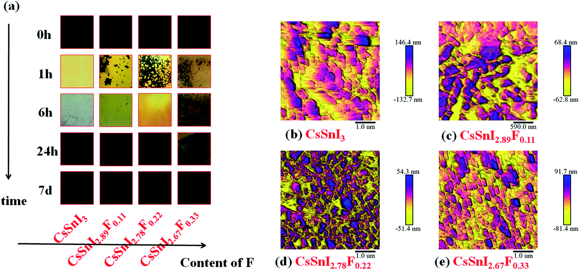 | ||
| Fig. 2 (a) Macroscopic images of the evolution in the cesium tin iodine doped fluorine (CsSnI3−xFx) films. (b–e) AFM images of the cesium tin iodine doped fluorine (CsSnI3−xFx) with different fluorine content, (b–e) correspond to CsSnI3, CsSnI2.89F0.11, CsSnI2.78F0.22, CsSnI2.67F0.33, respectively. | ||
3.2. Phase structure
Corroborating evidence for the process of phase transition in CsSnI3−xFx films \exposed in air was provided by X-ray diffraction (XRD), shown in Fig. 3a and b, which were consistent with the variations in morphology. Firstly, for the annealed CsSnI3−xFx films (see Fig. 3a), the peaks at 25.11°, 29.08° and 41.45° were attributed to B-γ-CsSnI3 phase (022), (220) and (224) planes (Ref.Code: 01-043-1162), respectively. Meanwhile, the well-matched peaks of 27.61° and 39.44°, assigned to CsI phase (110) and (200) planes (Ref.Code: 01-077-2185), were observed. However, the annealed XRD patterns also showed Y-CsSnI3 phase (111) and (121) planes (Ref.Code: 01-071-1898). The B-γ-CsSnI3 peaks of the annealed CsSnI3−xFx films became more distinct with the increase of F dopant ratios whilst the Y-CsSnI3 peaks became weaker. Although stoichiometric ratios were strictly controlled, the sharp and high intensity peaks of CsI also appeared in the XRD patterns, this can be attributed to incomplete reaction with SnI2, because SnI2 (vaporization point 993.15 K in ambient air) is easier to evaporate and decompose (unstable Sn2+) than CsI (vaporization point 1553 K in ambient air) in the process of thermal evaporation. The variations of the XRD patterns show that fluorine doping obstructed the transformation from B-γ-CsSnI3 to Y-CsSnI3 perovskite phases.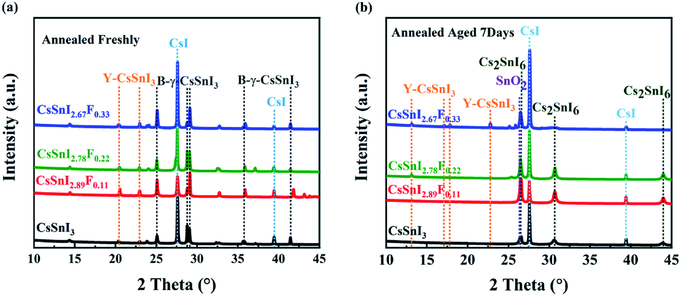 | ||
| Fig. 3 Evolution of XRD patterns of CsSnI3−xFx films with time. (a) XRD patterns of the CsSnI3−xFx films annealed freshly, (b) XRD patterns of the annealed CsSnI3−xFx films exposed in air for 7 days. | ||
After aging seven days in air, the films returned to a light black color. This phenomenon is consistent with the trend of Qiu's experiment.37 The new diffraction peaks (see Fig. 3b) at 26.44°, 30.61°, and 43.91° were attributed to the (222), (004) and (044) orientations of Cs2SnI6 phase (Ref.Code: 00-051-0466). However, the aged XRD patterns showed (120), (121), (130) and (210) planes of the Y-CsSnI3 phase. Furthermore, several diffraction peaks at 27.57°, 39.41°, and 26.58° assigned to CsI and SnO2 (Ref.Code: 00-077-0448) were observed as well. Again, the Y-CsSnI3 phase was much obvious with the increase of F dopant ratios, which meant F doping delayed the phase transformation, and Y phase existed in the highly F doped films even after aging for seven days.
Based on these findings via the above XRD data, partial CsI, SnI2, and SnO2 peaks were observed during the evolution process of the CsSnI3−xFx films, the chemical reactions involved may be as follows:

Therefore, it is clear that this process was due to oxidation of Sn in the compounds.6 Sn2+ ions are quite sensitive to external oxygen, especially in humid environments, which can be oxidized to more stable Sn4+ analogues. This oxidation process may fundamentally destroy the charge neutrality of the CsSnI3 perovskite structure and lead to phase transition. The Sn–F bonds form when fluorine replaces iodide in the lattice. The Sn–F bond length is shorter than that of Sn–I, resulting in a more stable crystal structure and weakening the role of oxygen, refer to Fig. S2.† In short, doping with fluorine slowed down the oxidation progress of the Sn2+ in CsSnI3 into Sn4+. The B-γ-CsSnI3−x(F)x phase eventually transferred into Cs2SnI6−x(F)x and was accompanied by the formation of SnO2 over time, but the formation processes are delayed by the additional F dopant. The remnant Y-CsSnI3 phase proved not only to delay the phase transition, but also the existence of Sn2+. The hybrid of Sn4+with Sn2+ resulted in the Cs2SnI6−x(F)x films showing their p type property.
3.3. Electrical properties of CsSnI3−xFx films
The electrical properties and thickness of the CsSnI3−xFx films at room temperature were measured by a HALL 8800 Hall Effect Measurement device and KLA-Tencor Alpha-step D-100 type profilometer respectively. The results were shown in Table 3 for the freshly annealed and Table 4 for those aged seven days after annealing. In this case, the thicknesses of the films were used to calculate the resistivity of the films. Both the annealed and aged CsSnI3−xFx films were p type semiconductors with the holes provided by the Sn vacancies. Intrinsic defects such as Sn vacancies in the ternary Cs–Sn–I system gave rise to p-type conductivity20 and DFT calculations have shown that the formation energy of VSn defects was the lowest among all defects.38 In Table 3, the freshly annealed CsSnI3 film exhibited the carrier densities of ∼1014 cm−3, and the carrier density of CsSnI3−xFx films increased to ∼1016 cm−3 with the increase of SnF2 content. It's also worth noting that the resistivities of CsSnI3−xFx films were 1–2 orders of magnitude smaller than that of undoped film. The reduction of the Sn vacancy concentrations can be attributed to the strong bonding energy between F and Sn.| Sample | Rs (Ω □−1) | ρ (Ω cm) | N/P (cm−3) | μ (cm2 V−1 s−1) | Thickness (nm) | Type |
|---|---|---|---|---|---|---|
| CsSnI3 | 2.14 × 10⁵ | 22.71 | 6.12 × 10¹⁴ | 449.31 | 1060 | P |
| CsSnI2.88F0.11 | 1.93 × 10⁴ | 4.65 | 5.84 × 10¹⁵ | 229.55 | 2410 | P |
| CsSnI2.78F0.22 | 4.99 × 10³ | 1.44 | 6.01 × 10¹⁶ | 226.67 | 2880 | P |
| CsSnI2.67F0.33 | 1.49 × 10³ | 0.394 | 7.29 × 10¹⁶ | 217.34 | 2650 | P |
| Sample | Rs (Ω □−1) | ρ (Ω cm) | N/P (cm−3) | μ (cm2 V−1 s−1) | Thickness (nm) | Type |
|---|---|---|---|---|---|---|
| CsSnI3 | 3.62 × 10⁵ | 38.75 | 1.42 × 10¹⁵ | 114.96 | 1060 | P |
| CsSnI2.88F0.11 | 4.07 × 10⁴ | 9.79 | 8.55 × 10¹⁵ | 74.55 | 2410 | P |
| CsSnI2.78F0.22 | 1.44 × 10⁴ | 4.16 | 6.21 × 10¹⁵ | 241.46 | 2880 | P |
| CsSnI2.67F0.33 | 3.54 × 10⁵ | 93.75 | 1.45 × 10¹⁶ | 4.59 | 2650 | P |
After aging in air for seven days, the electrical properties of the CsSnI3−xFx films kept the same order. As described in Section 3.2 Phase structure, the main composition of the CsSnI3−xFx films was Cs2SnI6. This is accompanied by the generation of a mass of Sn vacancies. The carrier densities of the aged CsSnI3−xFx films were almost at the same level in comparison to those of the annealed CsSnI3−xFx films. The resistivities of CsSnI3−xFx films were still relatively small. After aging for seven days, the phase transformation occurred, the oxidation of tin was completed, and the double layer ‘vacancy ordered’ phase Cs2SnI6−xFx formed. As the results, the Sn vacancies of the aged films were high, and their carrier density increased sharply. However, the rate of increase of the charge carriers of the aged films decreased with the increase of SnF2 content. The phases were stable due to F doping, the creation processes of the Sn vacancies were delayed and therefore, the changes of the electrical properties were slower. This fully illustrates SnF2 hindering the oxidation process of Sn2+, which blocked the formation of Cs2SnI6.
Since the carrier (hole or electron) concentration of semiconductor depends on the inherent defect concentration, the control of carrier concentration is a necessary condition to optimize the performance of solar cells. It works better as the hole-transport material (HTM) when hole concentration and conductivity are high, but it may work better as the light absorber material (LAM) when hole concentration and conductivity are moderate.39 From the data of electrical properties, by tuning the F doping amount, hole concentration and conductivity can be controlled, so that the film can be selectively arranged as HTM and LAM.
3.4. Optical properties
The absorptive spectra of the annealed and aged CsSnI3−xFx films within the range of 400–1400 nm were presented in Fig. 4a and c, respectively. Within the UV range, the absorptivity of the films was almost the same. The absorption edges of the annealed and aged CsSnI3−xFx films exhibited obvious differences. With the addition of SnF2, the light harvesting in the visible light region of the solar spectrum of the CsSnI3−xFx films was significantly enhanced. These differences indicate the difference of the band gap between samples. The spectra of the absorption via optical band gaps of the annealed and aged films were shown in Fig. 4b and d, which were calculated by the formula of αhθ = A(hθ − Eg)1/2. The Tauc plot40 is used to evaluate the optical energy gap. The bandgaps of all the CsSnI3−xFx films are between 1.25 eV and 1.3 eV as shown in Fig. 4b which was consistent with those previously reported.41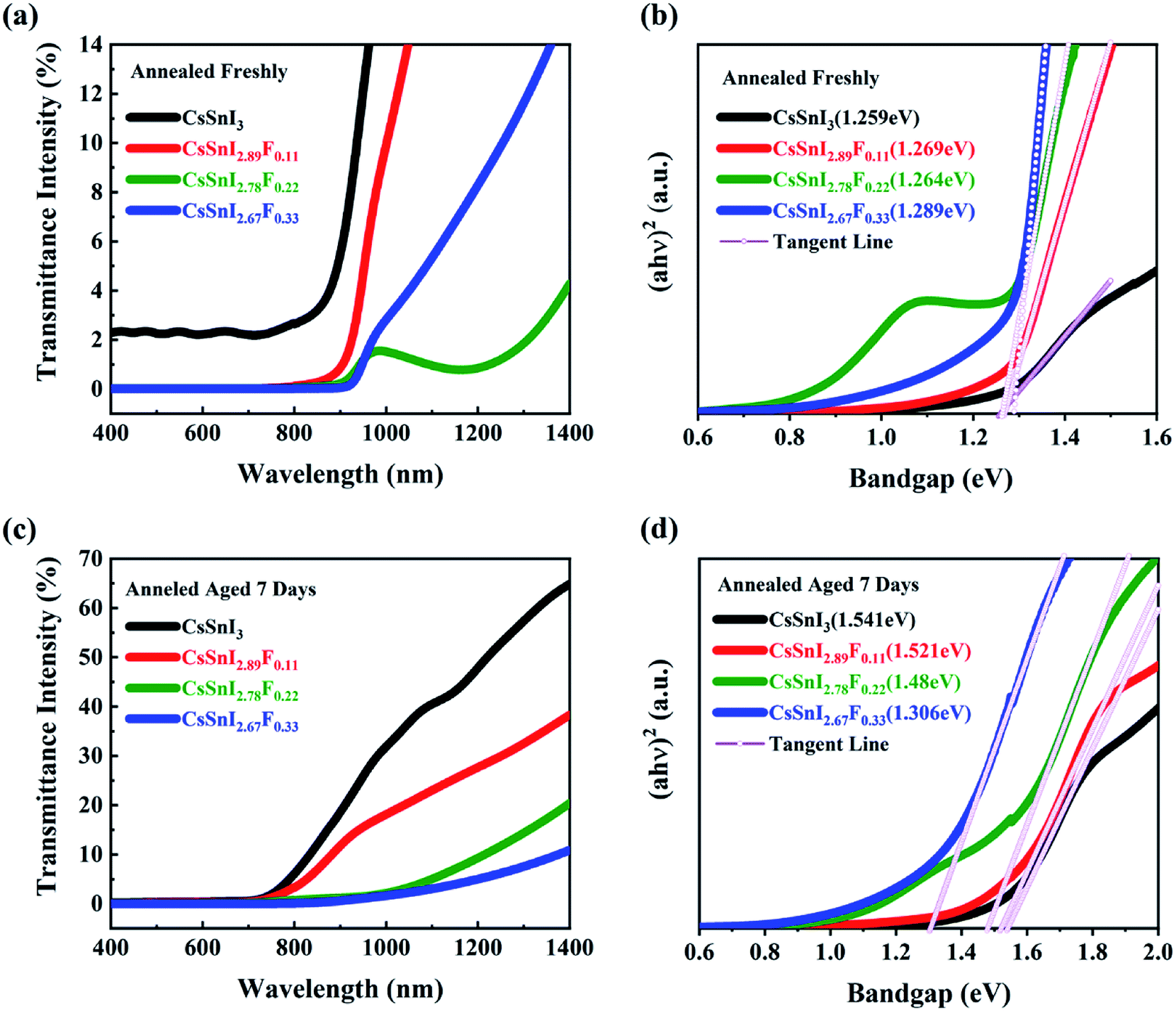 | ||
| Fig. 4 Optical spectra of CsSnI3−xFx films:(a and b) annealed freshly; (c and d) under exposure to ambient air for 7 days. | ||
The optical spectra of CsSnI3−xFx films under exposure to ambient air for seven days are shown in Fig. 4c and d. The absorption edges of all the CsSnI3−xFx films exhibited blue shift. All the bandgaps for the F doped films got smaller, and was close to 1.48 eV derived in Qiu's report.37 This is a result of SnF2 eliminating the formation of weak unidentified reflections due to the Y-CsSnI3 phase.42 After the CsSnI3−xFx films under exposure to ambient air for seven days, the Y-CsSnI3 phase only was shown in the highly F doped films, which the fully illustrates the role of SnF2. The transmittance of the Cs2SnI(F)6 films within visible wavelength were strongly affected by doping F ions due to the decomposition of CsSnI3−xFx. It was further shown that SnF2 blocked the formation of Cs2SnI6 by the changes of bandgap. Note that the sunlight absorption in the red and near-infrared regions has been a challenge for solar cells, and the excellent optical properties of CsSnI3−xFx films made up for this defect.
4. Conclusion
CsSnI3 transformed into stable double layer perovskite Cs2SnI6 phase in air was investigated for potential solar cell applications. By conducting a series of experiments, it was determined that the phase transformation in air can be slowed down by doping F ions into CsSnI3. The mechanism of phase transition delay is that Sn2+ preferentially bonds with F−, and thus the process of Sn2+ in CsSnI3 to be oxidized into Sn4+ was slowed down. The B-γ-CsSnI(F)3 phase eventually formed Cs2SnI(F)6 accompanied by the formation of the SnO2 phase over time, but the transition processes are delayed by the additional F dopant.Furthermore, SnF2 improved the carrier concentration and conductivity of the film, in which the resistivities of CsSnI3−xFx films were less than 10 Ω cm except CsSnI2.67F0.33. The CsSnI3−xFx films also absorbed more visible and infrared light with increased F doping than the pure CsSnI3 film. It was further shown that SnF2 blocked the formation of Cs2SnI6 by comparing the changes of bandgaps. The usage of CsSnI3−xFx films as HTM or LAM in solar cells is envisioned to be a promising method of improving efficiency.
Conflicts of interest
There are no conflicts to declare.Acknowledgements
The work at University of Science and Technology Liaoning is supported by National Natural Science Foundation of China (No. 51672119, 51774180, 51972155) and Royal Society International Exchanges 2017(IEC\NSFC\170535). Acknowledges go to the support from the Project of Young Teachers in the Higher Education Institutions of USTL (No. 2017QN13) and the Innovation Team Project of USTL (No. 2017TD01). Thanks go to the colleagues at Manchester Metropolitan University for their co-operation in this study.References
- A. Kojima, K. Teshima, Y. Shirai and T. Miyasaka, J. Am. Chem. Soc., 2009, 131, 6050–6051 CrossRef CAS PubMed.
- Q. Jiang, Y. Zhao, X. Zhang, X. Yang, Y. Chen, Z. Chu, Q. Ye, X. Li, Z. Yin and J. You, Nat. Photonics, 2019, 13, 460–466 CrossRef CAS.
- J. H. Im, H. S. Kim and N. G. Park, APL Mater., 2014, 2, 591–713 Search PubMed.
- I. Chung, B. Lee, J. He, R. P. Chang and M. G. Kanatzidis, Nature, 2012, 485, 486–489 CrossRef CAS PubMed.
- N. R. E. Laboratory, Best Research-Cell Efficiencies chart, http://www.nrel.gov/ncpv/images/efficiency_chart.jpg.
- C. C. Stoumpos, C. D. Malliakas and M. G. Kanatzidis, Inorg. Chem., 2013, 52, 9019–9038 CrossRef CAS PubMed.
- P. P. Boix, S. Agarwala, T. M. Koh, N. Mathews and S. G. Mhaisalkar, J. Phys. Chem. Lett., 2015, 6, 898–907 CrossRef CAS PubMed.
- P. Pyykko, Chem. Rev., 1988, 88, 563–594 CrossRef CAS.
- N. K. Noel, S. D. Stranks, A. Abate, C. Wehrenfennig, S. Guarnera, A. A. Haghighirad, A. Sadhanala, G. E. Eperon, S. K. Pathak and M. B. Johnston, Energy Environ. Sci., 2014, 7, 3061–3068 RSC.
- D. Moghe, L. Wang, C. J. Traverse, A. Redoute, M. Sponseller, P. R. Brown, V. Bulović and R. R. Lunt, Nano Energy, 2016, 28, 469–474 CrossRef CAS.
- L. Glasser, Inorg. Chem., 2012, 51, 2420 CrossRef CAS PubMed.
- K. Yamada, S. Funabiki, H. Horimoto, T. Matsui, T. Okuda and S. Ichiba, Chem. Lett., 1991, 20, 801–804 CrossRef.
- P. Mauersberger and F. Huber, Acta Crystallogr., Sect. B: Struct. Crystallogr. Cryst. Chem., 1980, 36, 683–684 CrossRef.
- A. E. Maughan, A. M. Ganose, M. M. Bordelon, E. M. Miller, D. O. Scanlon and J. R. Neilson, J. Am. Chem. Soc., 2016, 138, 8453–8464 CrossRef CAS PubMed.
- S. Vilminot, W. Granier, A. Soufiane, L. Cot, J. M. Letoffe and P. Claudy, Rev. Chim. Miner., 1985, 22, 125–133 CAS.
- T. Thao Tran and P. Shiv Halasyamani, J. Solid State Chem., 2014, 210, 213–218 CrossRef.
- W. B. Schaap, J. A. Davis and W. H. Nebergall, J. Am. Chem. Soc., 1954, 76, 5226–5229 CrossRef CAS.
- C. A. Randall, A. S. Bhalla, T. R. Shrout and L. E. Cross, J. Mater. Res., 1990, 5, 829–834 CrossRef CAS.
- T. M. Koh, T. Krishnamoorthy, N. Yantara, C. Shi, W. L. Leong, P. P. Boix, A. C. Grimsdale, S. G. Mhaisalkar and N. Mathews, J. Mater. Chem. A, 2015, 3, 14996–15000 RSC.
- M. H. Kumar, S. Dharani, W. L. Leong, P. P. Boix, R. R. Prabhakar, T. Baikie, C. Shi, H. Ding, R. Ramesh and M. Asta, Adv. Mater., 2014, 26, 7122–7127 CrossRef CAS PubMed.
- F. Hao, C. C. Stoumpos, P. Guo, N. Zhou, T. J. Marks, R. P. H. Chang and M. G. Kanatzidis, J. Am. Chem. Soc., 2015, 137, 11445–11452 CrossRef CAS PubMed.
- S. J. Lee, S. S. Shin, Y. C. Kim, D. Kim, T. K. Ahn, J. H. Noh, J. Seo and S. I. Seok, J. Am. Chem. Soc., 2016, 138, 3974–3977 CrossRef CAS PubMed.
- A. Dualeh, N. Tétreault, T. Moehl, P. Gao, M. K. Nazeeruddin and M. Grätzel, Adv. Funct. Mater., 2014, 24, 3250–3258 CrossRef CAS.
- G. E. Eperon, V. M. Burlakov, P. Docampo, A. Goriely and H. J. Snaith, Adv. Funct. Mater., 2014, 24, 151–157 CrossRef CAS.
- T. Leijtens, B. Lauber, G. E. Eperon, S. D. Stranks and H. J. Snaith, J. Phys. Chem. Lett., 2014, 5, 1096–1102 CrossRef CAS PubMed.
- W. Qi, Y. Shao, Q. Dong, Z. Xiao, Y. Yuan and J. Huang, Energy Environ. Sci., 2014, 7, 2359–2365 RSC.
- L. Po-Wei, L. Chien-Yi, C. Chu-Chen, Z. Fan, S. T. Williams, X. Xu-Kai, L. Jiangjen and J. K.-Y. Alex, Adv. Mater., 2014, 26, 3748–3754 CrossRef PubMed.
- Y. Zhao and K. Zhu, J. Phys. Chem. C, 2014, 118 Search PubMed.
- D. Shen, X. Yu, X. Cai, M. Peng, Y. Ma, X. Su, L. Xiao and D. Zou, J. Mater. Chem. A, 2014, 2, 20454–20461 RSC.
- S. Paek, N. Cho, H. Choi, H. Jeong, S. L. Jin, J. Y. Hwang, J. K. Lee and J. Ko, J. Phys. Chem. C, 2014, 118, 25899–25905 CrossRef CAS.
- K. Hak-Beom, C. Hyosung, J. Jaeki, K. Seongbeom, W. Bright, S. Seyeong and K. J. Young, Nanoscale, 2014, 6, 6679–6683 RSC.
- M. Liu, M. B. Johnston and H. J. Snaith, Nature, 2013, 501, 395 CrossRef CAS PubMed.
- Q. Chen, H. Zhou, Z. Hong, S. Luo, H. S. Duan, H. H. Wang, Y. Liu, G. Li and Y. Yang, J. Am. Chem. Soc., 2014, 136, 622–625 CrossRef CAS PubMed.
- B. Wu, Y. Zhou, G. Xing, Q. Xu, H. F. Garces, A. Solanki, T. W. Goh, N. P. Padture and T. C. Sum, Adv. Funct. Mater., 2017, 27, 1604818 CrossRef.
- X. R. Tong, Z. Zhao, J. S. Wu, Y. W. Zhou, P. Kelly and P. Gao, Nanosci. Nanotechnol. Lett., 2018, 10, 329–336 CrossRef.
- T. Degen, M. Sadki, E. Bron, U. Konig and G. Nenert, Powder Diffr., 2014, 29, S13–S18 CrossRef CAS.
- X. Qiu, B. Cao, Y. Shuai, X. Chen, Z. Qiu, Y. Jiang, Y. Qian, H. Wang, H. Zeng and L. Jian, Sol. Energy Mater. Sol. Cells, 2017, 159, 227–234 CrossRef CAS.
- I. Chung, J.-H. Song, J. Im, J. Androulakis, C. D. Malliakas, H. Li, A. J. Freeman, J. T. Kenney and M. G. Kanatzidis, J. Am. Chem. Soc., 2012, 134, 8579–8587 CrossRef CAS PubMed.
- Z. Xiao, Y. Zhou, H. Hosono and T. Kamiya, Phys. Chem. Chem. Phys., 2015, 17, 18900–18903 RSC.
- J. D. Neufville and H. Rockstad, 1974.
- L. Byunghong, C. C. Stoumpos, Z. Nanjia, H. Feng, M. Christos, Y. Chen-Yu, T. J. Marks, M. G. Kanatzidis and R. P. H. Chang, J. Am. Chem. Soc., 2014, 136, 15379–15385 CrossRef PubMed.
- Y. Zhou, H. F. Garces, B. S. Senturk, A. L. Ortiz and N. P. Padture, Mater. Lett., 2013, 110, 127–129 CrossRef CAS.
- S. Körbel, M. A. L. Marques and S. Botti, J. Mater. Chem. C, 2016, 4, 3157–3167 RSC.
Footnote |
| † Electronic supplementary information (ESI) available. See DOI: 10.1039/c9ra07415e |
| This journal is © The Royal Society of Chemistry 2019 |