DOI:
10.1039/C9RA07391D
(Paper)
RSC Adv., 2019,
9, 40792-40799
Nanopatterned silk fibroin films with high transparency and high haze for optical applications
Received
13th September 2019
, Accepted 30th November 2019
First published on
9th December 2019
Abstract
Simultaneous high transparency and high haze are necessary for high-efficiency optical, photonic, and optoelectronic applications. However, a typical highly transparent film lacks high optical haze or vice versa. Here, we report a silk fibroin-based optical film that exhibits both ultrahigh optical transparency (>93%) and ultrahigh optical transmission haze (>65%). Also, in combination with the soft lithography method, different nanostructured silk fibroin films are presented and their optical properties are characterized as well. To demonstrate its exceptional performance in both high transmission and high optical haze, we combine the silk fibroin with the silicon photodiode and show that the efficiency can be increased by 6.96% with the silk fibroin film without patterns and 14.9% with the nanopatterned silk fibroin film. Silk provides excellent mechanical, optical, and electrical properties, and the reported high-performance silk fibroin can enable the development of next-generation biocompatible eco-friendly flexible electronic and optical devices.
Introduction
Silk fibroin has excellent mechanical robustness, flexibility, optical transparency, bio-sustainability, biodegradability and environmental benignity, and is naturally abundant.1–6 In addition, silk fibroin provides solution processability and is compatible with the state-of-the-art nanomanufacturing technologies to create two dimensional or three-dimensional nanostructures, add new functionalities, and open new opportunities.7–12 Therefore, it is not surprising that silk fibroin has emerged as an attractive candidate for versatile applications.13–23
Substrate choice is increasingly crucial for optoelectronic systems. Currently, the optoelectronic industry mainly uses glass or plastic substrates for flexible electronic devices for their mechanical strength, optical transparency, and desirable processing temperature. However, with the mass production of electronic devices and their wide usage in our daily routine, they also generate a large amount of electronic waste containing toxic and nondegradable materials. To overcome this limitation, recently, silk fibroin has emerged as a promising alternative to existing plastic and glass substrates due to their environmental sustainability.24 Most existing applications of silk fibroin for flexible optical and electronic devices are focused on bio-integrated electronics, biodegradable electronics, biosensing, and so on.
Interestingly, in terms of optical properties, most of the aforementioned applications exploit the high transparency of the silk fibroin films. However, for photovoltaics, besides the high optical transparency, the high optical haze is equivalently essential. Optical haze is defined as the percentage of the forwarding transmitted light, diffusely scattering. The increased scattering can effectively improve solar cell efficiency, and it is desirable for photovoltaic applications.25–30 Therefore, optical films possessing both high transparency and high optical haze simultaneously are preferable for solar cell applications.
Consider that the β-sheet structures in silk fibroin can form nanofibers with a length about nanometers, which are widely distributed throughout the thin optical film. These fibril structures can effectively scatter light and supposedly increase the optical haze, while maintaining the high transparency. Therefore, in this study, we investigate the optical haze effect of the silk fibroin films and examine if the silk fibroin films exhibit both high optical transparency and high optical haze. In addition, since the silk fibroin can be patterned into different nanostructures via the standard soft lithography. The nanopatterned silk film provides us an excellent opportunity to engineer the optical response in terms of optical transmittance and optical haze by designing light-management silk fibroin-based nanostructures. Finally, to prove the concept, we integrate our engineered optical silk fibroin films with photodiodes by simply encapsulating them with the PDMS onto the photodiodes and demonstrate that they indeed can increase the power conversion efficiency due to the simultaneous high optical transmittance and high optical haze.
Results and discussion
Effect of degumming time
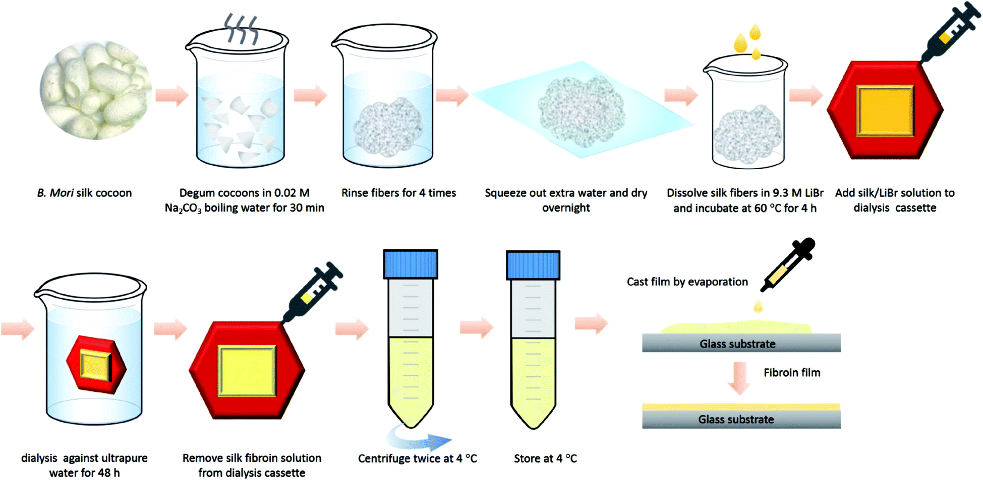
Here, we prepared silk fibroin proteins using the standard purification protocols (Fig. 1).31 In this process, degumming time is the key to prepare for the functional optical film. So first, we investigated the effect of degumming time on the peptide chain of silk fibroin. It is recognized that silk fibroin extracted from B. mori cocoons is composed of six heavy chains (around 390 kDa), six light chains (around 26 kDa), and a P25 chain (around 25 kDa).32–34 Different degumming time in the 0.02 M Na2CO3 solutions results in different molecular weight distribution of silk fibroin.2 Here, we chose 30 minutes for degumming since for optical applications presented here, we need to preserve the heavy chains as many as possible. However, if the degumming time is too short, the viscosity of the solution will be too high to fabricate the thin optical film. In addition, a longer degumming duration is necessary to remove sericin from raw silk to leave the pure silk fibroin for further processing.
 |
| | Fig. 1 The schematics of the silk fibroin extraction procedure. | |
FTIR-ATR molecular structure characterization of silk fibroin films
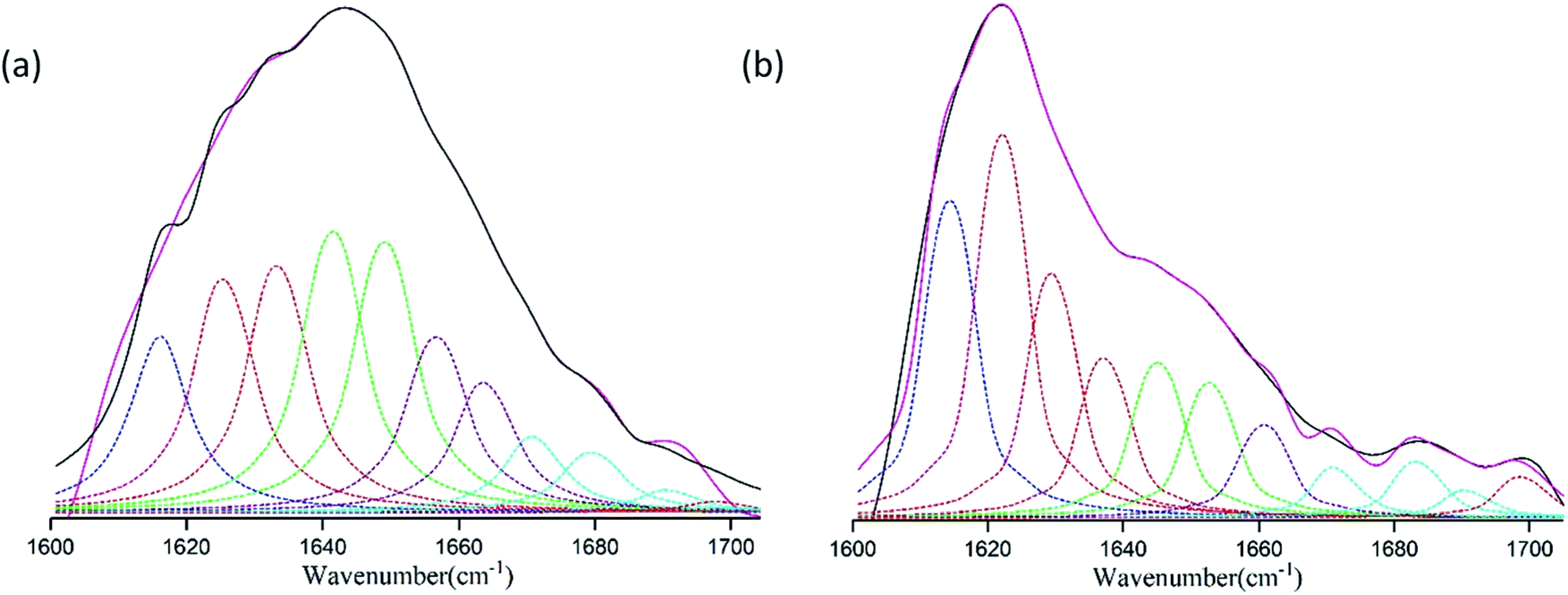
We used the Fourier Transform Infrared Spectroscopy (FTIR)-Attenuated Total Reflectance (ATR) to examine the molecular and crystalline structures of the fabricated silk fibroin optical film (Fig. 2). In Fig. 2, we show the FTIR-ATR for both untreated (a) and water-annealed (b) silk fibroin films. Here our focus is on amide I region from 1600 to 1708 cm−1.35 For this region, the vibrational band assignments are given in Table 1.
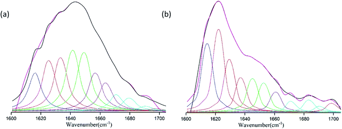 |
| | Fig. 2 The deconvolution of FTIR-ATR spectra for the amide I band for (a) untreated and (b) water-annealed silk fibroin films. | |
Table 1 Vibrational band assignments for the amide I region of silk fibroin36–38
| Wavenumber range (cm−1) |
Secondary structure assignment |
| 1605–1615 |
Side chains |
| 1616–1627 |
β-sheet |
| 1628–1637 |
β-sheet |
| 1638–1646 |
Random coils |
| 1647–1655 |
Random coils |
| 1656–1662 |
α-helix |
| 1663–1672 |
Turns |
| 1673–1685 |
Turns |
| 1686–1695 |
Turns |
| 1697–1703 |
β-sheet (weak) |
To estimate the conformation contents of each secondary structure, we deconvolved the FTIR spectra and integrated the area underneath each deconvolved peaks.37 Briefly, here we used the secondary-derivative analysis to find the peak positions.39 The deconvoluted peak shapes are assumed to be Lorentzian.36,40 The percentages of corresponding silk fibroin secondary structures are listed in Table 2. Table 2 shows that water annealing can significantly increase the β-sheet percentage and make β-sheet a predominance of the secondary structure.41,42
Table 2 The relative ratio of secondary structures in the regenerated silk fibroin film
| Silk secondary structure |
Untreated (% content) |
Water-annealed (% content) |
| Side chains |
9.6 |
18.6 |
| β-sheet |
29.1 |
49.8 |
| Random coils |
33.6 |
17.9 |
| α-helix |
18.5 |
5.8 |
| Turns |
9.2 |
7.9 |
Nanopatterned silk fibroin films
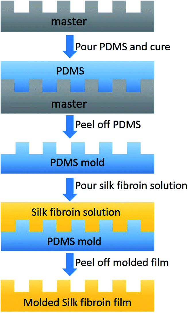
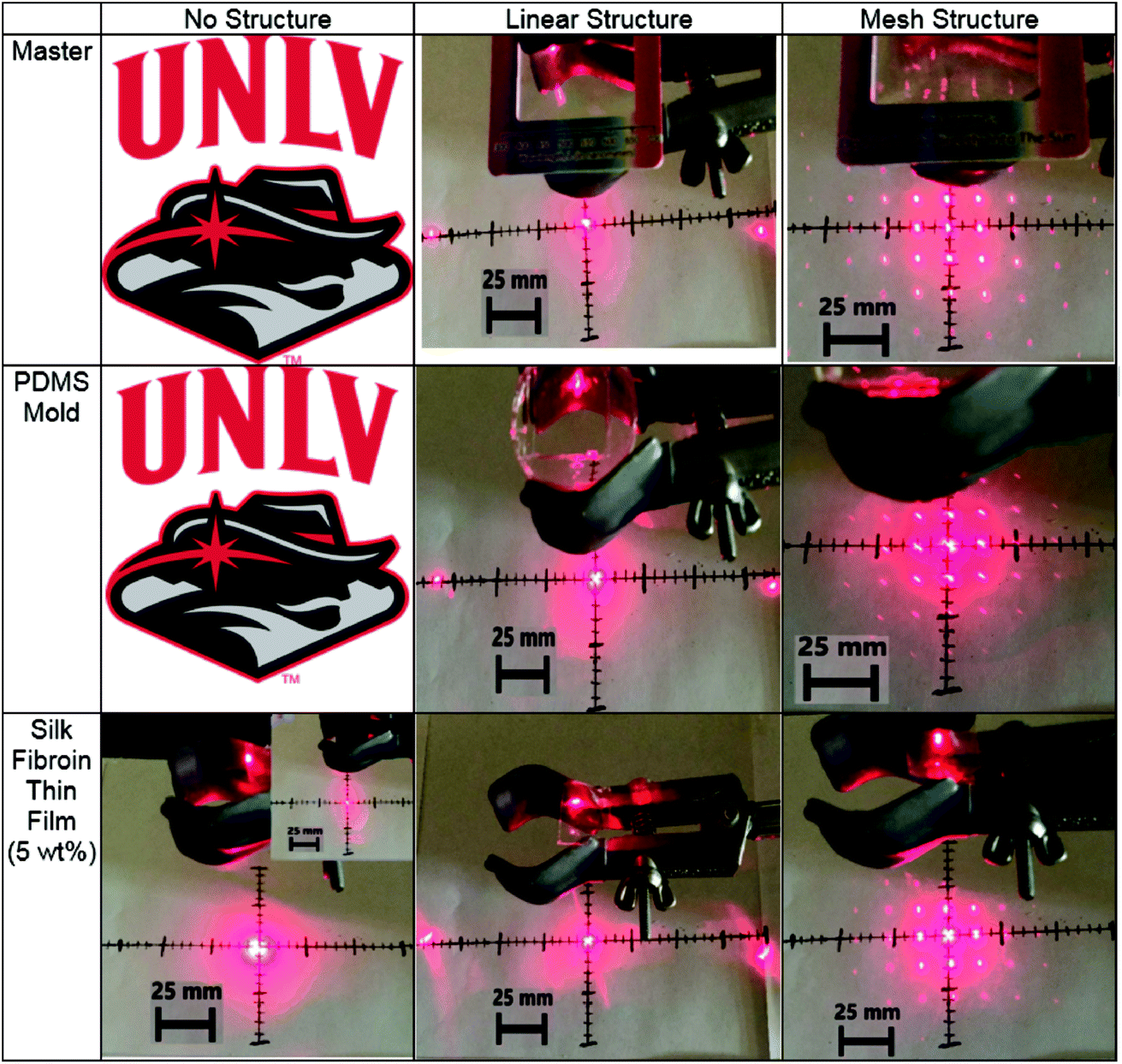
We used the standard soft lithography43 to pattern nanostructures made from silk fibroin (Fig. 3). The diffraction grating with a linear structure of 1000 lines per mm and a mesh structure of 13![[thin space (1/6-em)]](https://www.rsc.org/images/entities/char_2009.gif) 500 lines per inch were used for replication. We first used the soft lithography to create the PDMS molds by replicating them from the patterns. Then, the regenerated silk fibroin solution can be casted into the PDMS molds and the final nanostructured silk fibroin films were fabricated. Fig. 4 shows the light scattering effects by the laser with a wavelength of 650 nm for no structures, linear structures, and mesh structures from the masters, the PDMS molds, and the silk fibroin films. The light was passed through the samples 10 cm above a target with minor axis tick marks of 5 mm and major axis tick marks of 25 mm to help estimate the optical transmission haze effect. The same behavior of the light scattering of the samples from the masters, the PDMS molds, and the regenerated silk fibroin films suggests that the structures were well replicated onto silk fibroin films.
500 lines per inch were used for replication. We first used the soft lithography to create the PDMS molds by replicating them from the patterns. Then, the regenerated silk fibroin solution can be casted into the PDMS molds and the final nanostructured silk fibroin films were fabricated. Fig. 4 shows the light scattering effects by the laser with a wavelength of 650 nm for no structures, linear structures, and mesh structures from the masters, the PDMS molds, and the silk fibroin films. The light was passed through the samples 10 cm above a target with minor axis tick marks of 5 mm and major axis tick marks of 25 mm to help estimate the optical transmission haze effect. The same behavior of the light scattering of the samples from the masters, the PDMS molds, and the regenerated silk fibroin films suggests that the structures were well replicated onto silk fibroin films.
 |
| | Fig. 3 The schematics of the fabrication procedure to pattern nanostructures onto the silk fibroin film. | |
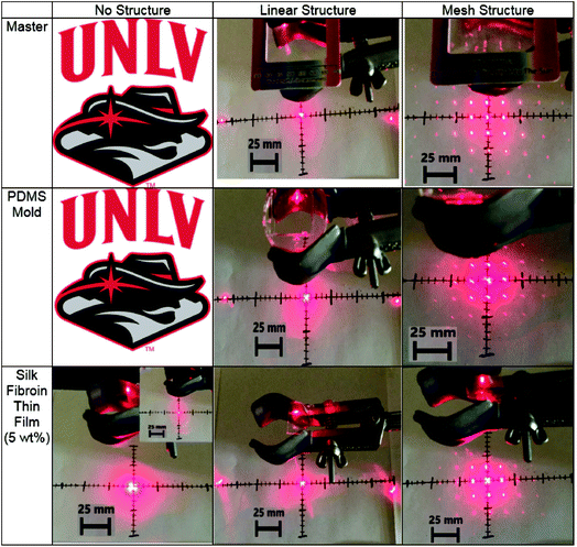 |
| | Fig. 4 The light scattering of the master, PDMS mold, and the patterned silk fibroin film with the laser light test. | |
Optical characterization
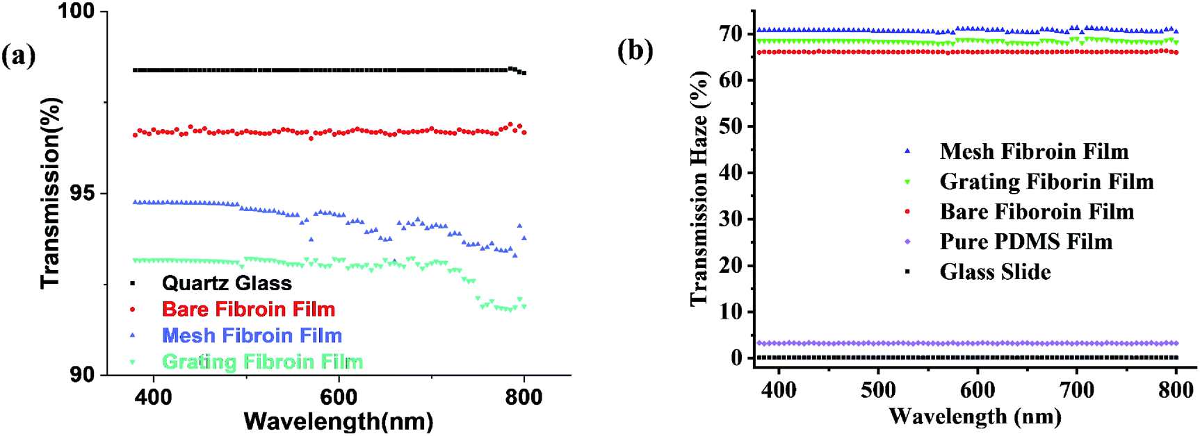
Optical thin films with high transmission and high transmission haze can find important applications in optoelectronic devices. The optical transmittance and the optical haze were measured by the Jasco V670 with the integrated sphere. To quantify optical properties, Fig. 5 plots the transmittance and transmission optical haze as a function of the wavelength for the glass (the reference), the flat PDMS, the flat silk fibroin film without patterns, the linear structured silk fibroin film, and the one with the mesh structure. All the regenerated silk fibroin films exhibit a transmittance higher than 93% where the flat silk fibroin film has the highest transmittance above 96%. The silk fibroin films also simultaneously demonstrate the high optical transmission haze (>65%) in which the one with the mesh structure has the highest (∼70%). The optical haze can also be visualized by the laser. In Fig. 4 (the lower left), the laser light displays a hazy circular cloud surrounding the point of about 25 mm radius as it is transmitted through the film. With the laser point by itself in the corner of the bottom left photo of Fig. 4, it can be seen the light is within a circle of a 5 mm radius. The increase of the illumination area is attributed to the high optical transmission haze. The high optical haze can be attributed to the secondary structures of regenerated silk fibroin including β-sheet and random coils which consist of about 67.7% of the silk fibroin secondary structures.44–46 Fig. 6 shows the SEM images of the random arrangement of silk nanofibrils in the silk fibroin film. The random distribution of these fiber-like network structures can effectively scatter light to achieve high optical haze.47,48
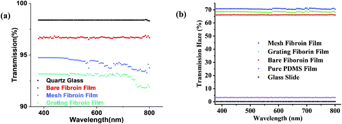 |
| | Fig. 5 The transmittance (a) and the optical transmission haze (b) as a function of the wavelength for various films. | |
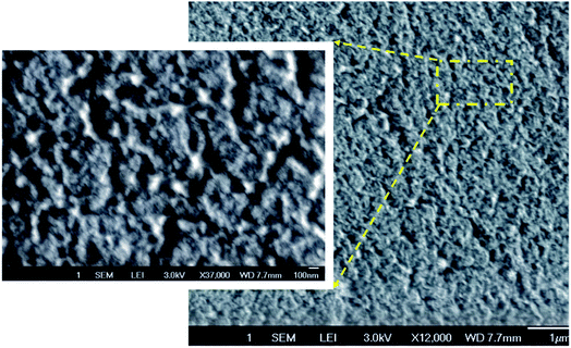 |
| | Fig. 6 The SEM images of random arrangement of silk nanofibrils in the silk fibroin film. | |
Applications in silicon photodiodes
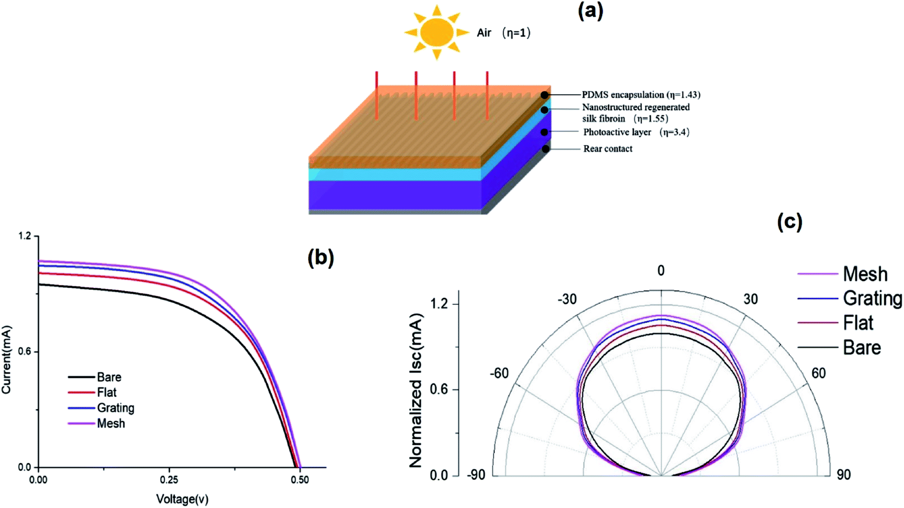
Regenerated silk fibroin films with high transmittance and high optical transmission haze can find important applications in optoelectronic devices. Particularly, they can increase the path of light traveling by front scattering to enhance light absorption. To prove this concept, we encapsulated the regenerated silk fibroin films with the PDMS onto amorphous silicon photodiodes (Fig. 7a). We recorded the I–V curves of the silicon photodiodes without and with the flat silk fibroin film, the silk fibroin film with the linear and mesh structures under the solar simulator with 1 Sun AM 1.5 G illumination. Fig. 7b suggests that our fabricated mesh-structure silk fibroin films can enhance the efficiency of photodiodes by 14.9% with the flat silk fibroin film increasing the efficiency by 6.96% mainly via decreasing the reflection and increasing the light scattering due to the combination of high transmittance and high optical transmission haze effect. Interestingly, the refractive index of silk fibroin is 1.55 at the wavelength of 500 nm.5,49 The refractive index of the PDMS is 1.43 at the wavelength of 400 nm. A gradual increase of the refractive index from the air to the silicon layer can minimize the reflection loss (Fig. 7a).50,51 In other words, beside the high haze effect, the gradual change of the refractive index by silk fibroin helps to improve the photodiode efficiency as well.
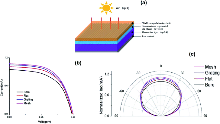 |
| | Fig. 7 (a) The schematics of the photodiode coated with the silk fibroin film; (b) The I–V curves of silicon photodiodes without (the black solid line) and with the encapsulated silk fibroin films; (c) the angular dependence of a normalized photocurrent without (the black solid line) and with encapsulated silk fibroin films, showing omnidirectional optical properties. | |
In addition, we measured the angular dependence of the photocurrent response by rotating the device gradually to generate various incident angles (Fig. 7c). Here, the incident angle refers to the one between the incident light and the normal direction of the encapsulated film. To better demonstrate the enhancement, we normalized the photocurrent of the one without the silk fibroin film with a zero-incident angle. Fig. 7c indicates that a larger enhancement of the photocurrent was achieved over a wide range of incident angles. The omnidirectional photocurrent improvement can be attributed to the broadened angular distribution of the scattered incident light by the silk fibroin film. The photocurrent enhancement at various incident angles suggests that the regenerated silk fibroin films can further improve the performance of the optoelectronic devices, by effectively collecting the ambient light more efficiently. This omnidirectional property is particularly attractive for photovoltaic applications where sun light is needed to be collected from all different directions throughout the day.
Conclusions
Here we fabricated the regenerated silk fibroin films from B. mori cocoons and patterned them into different nanostructures via the soft lithography. We characterized the optical properties of the flat regenerated silk fibroin film without patterns, the one with the linear structure, and the one with the mesh structure. They all demonstrated high optical transmittance and high optical transmission haze simultaneously though the optical properties can be tuned by designed structures. High transmission and high optical haze can find important applications in photoelectronic devices i.e. photovoltaics and photodiodes where broadband and omnidirectional light trapping is desirable. In fact, by encapsulating the silk fibroin films onto the silicon photodiodes, the power conversion efficiency can be increased by over 14.94% for the mesh structure. Showcasing the optical capability of the nanopatterned regenerated silk fibroin films opens new paths for research regarding this protein and new applications that have previously not been considered. This abundant and environmentally benign biomaterial can revolutionize the relevant optoelectronic fields as it is a smarter material option for the environment and it is applicable to many optical applications.
Finally, we need to emphasize that here we chose photodiodes as a proof of concept to show that patterned silk fibroin films can find applications in optoelectronics. But for the more useful applications and broader impacts, it is more interesting to integrate patterned silk fibroin films with biodegradable solar cells to provide power source for next-generation biomedical devices for active diagnostic or therapeutic function. Recent studies showed that biodegradable monocrystalline silicon photovoltaic microcells can be power supplies for transient biomedical implants52 and organic photovoltaics can be integrated to power cardiac signal detection.53 Silk fibroin films are compatible with these biodegradable photovoltaic systems and may improve their efficiency, which is beyond the scope of this work but deserves further attentions.
Materials and methods
Preparation of the silk fibroin aqueous solution
Silk fibroin solution was prepared as previously reported.31 Briefly, B. mori cocoons were cut into small pieces and rinsed with ultra-purified water with a specific resistivity of 18.2 MΩ cm (PURELAB Classic, ELGA LabWater, LLC). After drying, 2.5 gram cocoons were added to 1 L of boiling 0.02 M sodium carbonate (Na2CO3) (Sigma Aldrich) for degumming 15 min, 30 min, and 60 min, respectively to examine the effect of the degumming time. After degumming, the remaining fibroin bundle was rinsed with ultra-purified water thoroughly and dried overnight. The dried fibroin bundle was then dissolved in a 9.3 M lithium bromide (LiBr) solution with a ratio of 1 to 4. Then we put them in a water bath at 60 °C for at least 4 hours. After being fully dissolved, the solution was then dialyzed against 1 L of ultra-purified water (water was changed after 1, 4, 8, 12, 24, 36, and 40 hours) with a 3–12 mL dialysis cassette (3500 MWCO). The solution was then centrifuged to remove insoluble impurities and the final purified silk fibroin solution was stored at 4 °C for further usage.
Fourier transform infrared (FTIR)/Attenuated total reflectance (ATR)
All FTIR measurements were performed using a BIO-RAD FTS-7000 spectrometer with a germanium horizontal attenuated total reflectance attachment attached to the UMA 600 microscope in the rapid scan mode (Bio-Rad). The parameters utilized included a frequency of 2.5 kHz, a filter setting of 1.2, and a UDR setting of 2 for all samples. Each sample was scanned 64 times with a resolution setting of 4 cm−1 or 8 cm−1 and averaged to produce each spectrum. All samples were examined using multiple points of contact to ensure consistency. The data was not subjected to any smoothing.
Silk fibroin films
We dropped the regenerated silk fibroin solution onto the top of the substrate and let it dry to form a thin film. To improve the film's mechanical and chemical properties, we used the water annealing method.14,36,54 Briefly, the dry film was placed into a vacuum desiccator filled with water in the bottom and the pump was turned on to extract the air out. This exposes the film to an extremely high humidity environment and promotes β-sheet crystal structure. The film was kept like this for at least a day. Upon removing the film from the vacuum desiccator chamber, the film is extremely soft, flexible, and stretchable.
Nanostructured silk fibroin films
Here we used the soft lithography to pattern nanostructures onto the regenerated silk fibroin films. We chose a polyester film (PET film) featuring a linear structure (1000 lines per mm) and a mesh structure (13500 lines per inch) as masters for replication. First, we used the standard soft lithography to create the PDMS mold. Here PDMS was mixed at a 10:1 ratio with the curing agent. Then, the PDMS solution was cast onto the PET film, which can then be set in an oven to cure at 80 °C for 3 hours. Then the PET film can be removed, and the PDMS mold with the featured structures was replicated.
To create the patterned regenerated silk fibroin film, the silk fibroin solution was cast onto the PDMS mold. The solution was left on the mold for about 3–4 hours at room temperature until fully dried. Then the PDMS mold can be removed. Finally, the patterned silk fibroin films were placed into the vacuum desiccator for water annealing treatment.
Photoelectronic characterization
Silicon photodiodes were purchased from OSRA-SMT DOL. Photodiodes were pinned into a thick PDMS substrate to coat the silk fibroin film. We sprayed ethanol on the photodiode's surface to assure that the regenerated silk fibroin film was fully attached. Next, the PDMS solution was poured on the film to encapsulate the photodiodes. The photodiodes with and without the regenerated silk fibroin films were tested with the Newport Sun simulator (940X1 Oriel instrument) with the AM 1.5 G sunlight spectrum filter by using OSRAM XBO 1000 watt/HS OFR. The current–voltage curves of the devices were measured under these conditions by applying two multimeters (Agilent 34405A and Keithley 6514 system) by adjusting the resistance gradually. The data were accurate to four decimal places.
Conflicts of interest
There are no conflicts to declare.
References
- L. D. Koh, Y. Cheng, C. P. Teng, Y. W. Khin, X. J. Loh, S. Y. Tee, M. Low, E. Ye, H. D. Yu, Y. W. Zhang and M. Y. Han, Prog. Polym. Sci., 2015, 46, 86–110 CrossRef CAS.
- B. P. Partlow, A. P. Tabatabai, G. G. Leisk, P. Cebe, D. L. Blair and D. L. Kaplan, Macromol. Biosci., 2016, 16, 666–675 CrossRef CAS PubMed.
- T. Asakura, K. Okushita and M. P. Williamson, Macromolecules, 2015, 48, 2345–2357 CrossRef CAS.
- Y. Cao and B. Wang, Int. J. Mol. Sci., 2009, 10, 1514–1524 CrossRef CAS PubMed.
- G. Perotto, Y. Zhang, D. Naskar, N. Patel, D. L. Kaplan, S. C. Kundu and F. G. Omenetto, Appl. Phys. Lett., 2017, 111, 103702 CrossRef.
- L. S. Wray, X. Hu, J. Gallego, I. Georgakoudi, F. G. Omenetto, D. Schmidt and D. L. Kaplan, J. Biomed. Mater. Res., Part B, 2011, 99, 89–101 CrossRef PubMed.
- H. Perry, A. Gopinath, D. L. Kaplan, L. D. Negro and F. G. Omenetto, Adv. Mater., 2008, 20, 3070–3072 CrossRef CAS.
- J. J. Amsden, P. Domachuk, A. Gopinath, R. D. White, L. D. Negro, D. L. Kaplan and F. G. Omenetto, Adv. Mater., 2010, 22, 1746–1749 CrossRef CAS PubMed.
- J. J. Amsden, H. Perry, S. V Boriskina, A. Gopinath, D. L. Kaplan, L. Dal Negro and F. G. Omenetto, Opt. Express, 2009, 17, 21271 CrossRef CAS PubMed.
- B. D. Lawrence, M. Cronin-Golomb, I. Georgakoudi, D. L. Kaplan and F. G. Omenetto, Biomacromolecules, 2008, 9, 1214–1220 CrossRef CAS PubMed.
- S. Kim, B. Marelli, M. A. Brenckle, A. N. Mitropoulos, E. S. Gil, K. Tsioris, H. Tao, D. L. Kaplan and F. G. Omenetto, Nat. Nanotechnol., 2014, 9, 306–310 CrossRef CAS PubMed.
- J. Zhong, M. Ma, J. Zhou, D. Wei, Z. Yan and D. He, ACS Appl. Mater. Interfaces, 2013, 5, 737–746 CrossRef CAS PubMed.
- C. Y. Zhang, J. Gao and Z. Wang, Adv. Mater., 2018, 1803618 CrossRef PubMed.
- D. J. Hines and D. L. Kaplan, Biomacromolecules, 2011, 12, 804–812 CrossRef CAS PubMed.
- O. Etienne, A. Schneider, J. A. Kluge, C. Bellemin-Laponnaz, C. Polidori, G. G. Leisk, D. L. Kaplan, J. A. Garlick and C. Egles, J. Periodontol., 2009, 80, 1852–1858 CrossRef PubMed.
- X. Wang, H. J. Kim, P. Xu, A. Matsumoto and D. L. Kaplan, Langmuir, 2005, 21, 11335–11341 CrossRef CAS PubMed.
- H. Tao, B. Marelli, M. Yang, B. An, M. S. Onses, J. A. Rogers, D. L. Kaplan and F. G. Omenetto, Adv. Mater., 2015, 27, 4273–4279 CrossRef CAS PubMed.
- H. J. Jin, J. Park, R. Valluzzi, P. Cebe and D. L. Kaplan, Biomacromolecules, 2004, 5, 711–717 CrossRef CAS PubMed.
- R. Nazarov, H.-J. Jin and D. L. Kaplan, Biomacromolecules, 2004, 5, 718–726 CrossRef CAS PubMed.
- S. H. Kim, Y. S. Nam, T. S. Lee and W. H. Park, Polym. J., 2003, 35, 185–190 CrossRef CAS.
- T. Yucel, M. L. Lovett and D. L. Kaplan, J. Controlled Release, 2014, 190, 381–397 CrossRef CAS PubMed.
- Y. S. Zhang and A. Khademhosseini, Science, 2017, 356 CAS.
- Y. Huang, K. Bailey, S. Wang and X. Feng, React. Funct. Polym., 2017, 116, 57–68 CrossRef CAS.
- H. Tao, D. L. Kaplan and F. G. Omenetto, Adv. Mater., 2012, 24, 2824–2837 CrossRef CAS PubMed.
- M. A. Tsai, P. Yu and H. C. Kuo, Conf. Rec. IEEE Photovoltaic Spec. Conf., 2011, 000683–000685 Search PubMed.
- M. Petrov, K. Lovchinov, M. Mews, C. Leendertz and D. Dimova-Malinovska, J. Phys.: Conf. Ser., 2014, 559, 12018 CrossRef.
- Z. Fang, H. Zhu, Y. Yuan, D. Ha, S. Zhu, C. Preston, Q. Chen, Y. Li, X. Han, S. Lee, G. Chen, T. Li, J. Munday, J. Huang and L. Hu, Nano Lett., 2014, 14, 765–773 CrossRef CAS PubMed.
- G. Kang, K. Bae, M. Nam, D. H. Ko, K. Kim and W. J. Padilla, Energy Environ. Sci., 2015, 8, 2650–2656 RSC.
- I. Hwang, D. Choi, S. Lee, J. H. Seo, K. H. Kim, I. Yoon and K. Seo, ACS Appl. Mater. Interfaces, 2017, 9, 21276–21282 CrossRef CAS PubMed.
- S. Zhai, Y. Zhao and H. Zhao, ACS Appl. Mater. Interfaces, 2019, 11, 12978–12985 CrossRef CAS PubMed.
- D. D. N. Rockwood, R. R. C. Preda, T. Yücel, X. Wang, M. L. Lovett and D. L. Kaplan, Nat. Protoc., 2011, 6, 1–43 CrossRef PubMed.
- C. Z. Zhou, F. Confalonieri, M. Jacquet, R. Perasso, Z. G. Li and J. Janin, Proteins: Struct., Funct., Genet., 2001, 44, 119–122 CrossRef CAS PubMed.
- S. Inoue, K. Tanaka, F. Arisaka, S. Kimura, K. Ohtomo and S. Mizuno, J. Biol. Chem., 2000, 275, 40517–40528 CrossRef CAS PubMed.
- C. Vepari and D. L. Kaplan, Prog. Polym. Sci., 2007, 32, 991–1007 CrossRef CAS PubMed.
- D. M. Byler, H. Susi and E. Regional, Biopolymers, 1986, 25, 469–487 CrossRef CAS PubMed.
- X. Hu, D. Kaplan and P. Cebe, Macromolecules, 2006, 39, 6161–6170 CrossRef CAS.
- B. D. Lawrence, F. Omenetto, K. Chui and D. L. Kaplan, J. Mater. Sci., 2008, 43, 6967–6985 CrossRef CAS.
- Q. Lu, X. Hu, X. Wang, J. A. Kluge, S. Lu, P. Cebe and D. L. Kaplan, Acta Biomater., 2010, 6, 1380–1387 CrossRef CAS PubMed.
- H. Yang, S. Yang, J. Kong, A. Dong and S. Yu, Nat. Protoc., 2015, 10, 382–396 CrossRef CAS PubMed.
- O. N. Tretinnikov and Y. Tamada, Langmuir, 2001, 17, 7406–7413 CrossRef CAS.
- H. J. Jin, J. Park, V. Karageorgiou, U. J. Kim, R. Valluzzi, P. Cebe and D. L. Kaplan, Adv. Funct. Mater., 2005, 15, 1241–1247 CrossRef CAS.
- H. J. Jin and D. L. Kaplan, Nature, 2003, 424, 1057–1061 CrossRef CAS PubMed.
- Y. Xia and G. M. Whitesides, Annu. Rev. Mater. Sci., 1998, 28, 153–184 CrossRef CAS.
- Z. Liu, F. Zhang, J. Ming, S. Bie, J. Li and B. Zuo, J. Appl. Polym. Sci., 2014, 132, 1–7 Search PubMed.
- F. Zhang, Q. Lu, J. Ming, H. Dou, Z. Liu, B. Zuo, M. Qin, F. Li, D. L. Kaplan and X. Zhang, J. Mater. Chem. B, 2014, 2, 3879–3885 RSC.
- F. Zhang, X. You, H. Dou, Z. Liu, B. Zuo and X. Zhang, ACS Appl. Mater. Interfaces, 2015, 7, 3352–3361 CrossRef CAS PubMed.
- Z. Fang, H. Zhu, C. Preston, X. Han, Y. Li, S. Lee, X. Chai, G. Chen and L. Hu, J. Mater. Chem. C, 2013, 1, 6191–6197 RSC.
- H. Zhu, Z. Fang, Z. Wang, J. Dai, Y. Yao, F. Shen, C. Preston, W. Wu, P. Peng, N. Jang, Q. Yu, Z. Yu and L. Hu, ACS Nano, 2016, 10, 1369–1377 CrossRef CAS PubMed.
- E. Colusso, G. Perotto, Y. Wang, M. Sturaro, F. Omenetto and A. Martucci, J. Mater. Chem. C, 2017, 5, 3924–3931 RSC.
- E. Baquedano, L. Torné, P. Caño and P. A. Postigo, Nanomaterials, 2017, 7, 437 CrossRef PubMed.
- S. B. Khan, S. Irfan, Z. Zhuanghao and S. L. Lee, Materials, 2019, 12, 1483 CrossRef PubMed.
- L. Lu, Z. Yang, K. Meacham, C. Cvetkovic, E. A. Corbin, A. Vázquez-Guardado, M. Xue, L. Yin, J. Boroumand, G. Pakeltis, T. Sang, K. J. Yu, D. Chanda, R. Bashir, R. W. Gereau, X. Sheng and J. A. Rogers, Adv. Energy Mater., 2018, 8, 1703035 CrossRef.
- S. Park, S. W. Heo, W. Lee, D. Inoue, Z. Jiang, K. Yu, H. Jinno, D. Hashizume, M. Sekino, T. Yokota, K. Fukuda, K. Tajima and T. Someya, Nature, 2018, 561, 516–521 CrossRef CAS PubMed.
- Z. Zhou, Z. Shi, X. Cai, S. Zhang, S. G. Corder, X. Li, Y. Zhang, G. Zhang, L. Chen, M. Liu, D. L. Kaplan, F. G. Omenetto, Y. Mao, Z. Tao and T. H. Tao, Adv. Mater., 2017, 29, 1–7 Search PubMed.
Footnote |
| † Both authors contributed equally to this work. |
|
| This journal is © The Royal Society of Chemistry 2019 |
Click here to see how this site uses Cookies. View our privacy policy here. 
 Open Access Article
 This Open Access Article is licensed under a Creative Commons Attribution-Non Commercial 3.0 Unported Licence
 *a
*a