
 Open Access Article
 This Open Access Article is licensed under a Creative Commons Attribution-Non Commercial 3.0 Unported Licence
Interface chemistry and leakage current mechanism of HfGdON/Ge gate stack modulated by ALD-driven interlayer
Gang He *ab,
Die Wanga,
Rui Mac,
Mao Liu*c and
Jingbiao Cuid
*ab,
Die Wanga,
Rui Mac,
Mao Liu*c and
Jingbiao Cuid
aSchool of Physics and Materials Science, Radiation Detection Materials & Devices Lab, Anhui University, Hefei 230601, P. R. China. E-mail: hegang@ahu.edu.cn
bInstitute of Physical Science and Information Technology, Anhui University, Hefei 230601, P. R. China
cKey Laboratory of Materials Physics, Anhui Key Laboratory of Nanomaterials and Nanostructures, Institute of Solid State Physics, Chinese Academy of Sciences, Hefei 230031, P. R. China. E-mail: mliu@issp.ac.cn
dDepartment of Physics, University of North Texas, Denton, TX76203, USA
First published on 21st October 2019
Abstract
In current manuscript, a Ge metal-oxide-semiconductor (MOS) capacitor based on HfGdON/Ge gate stacks with an ALD-driven passivation layer has been fabricated, and its interfacial and electrical properties are compared with those of its counterparts that have not undergone passivation treatment. Electrical analyses revealed that the HfGdON/Al2O3/Ge MOS device exhibits improved performance, including larger permittivity, negligible hysteresis, reduced flat band voltage, good capacitance–voltage behavior, and lower interface state and border trapped oxide charge density. All of these improvements can be ascribed to the suppressed growth of unstable Ge oxides, thus reducing the defective states at or near the HfGdON/Ge interface and improving the interface quality. In addition, detailed analyses of the current conduction mechanisms (CCMs) for Ge MOS capacitors with different passivation treatment were investigated systematically.
1. Introduction
Germanium (Ge) has been attracting increasing attention as a channel material in metal-oxide-semiconductor field-effect transistors (MOSFETs), owing to its high carrier mobility, resulting in a large drive current, and small band gap for supply voltage scaling, as compared to the conventional Si channel material.1–3 However, the absence of a high-quality MOS interface, such as the SiO2/Si interface, has inhibited the development of Ge-based MOSFET devices, due to the volatility of GeOx species.3,4 One important challenge associated with Ge-MOSFETs is the formation of native oxide on the Ge surface, resulting in an extremely high density of interface states (Dit) and Fermi-level pinning at the high-k/Ge interface. Therefore, achieving a high-quality and thermodynamically stable insulator on Ge needs to be realized for the successful application of Ge-based MOSFETs.To address this issue, the use of different surface-passivation techniques on Ge substrates upon gate stack formation has been intensively explored to prevent the performance degradation of Ge-based MOSFETs, such as surface nitridation,5 sulfur passivation,6 high-quality epitaxial layer growth,7 and the adoption of various passivation layers, e.g. GeO2, SiO2, and rare earth oxides.8–10 However, nitridation treatment usually requires high temperatures, which limits the thermal budget. For sulfur passivation, the formation of large surface states in the Ge energy band gap renders elemental S passivation less desirable for high-performance MOSFET devices.11 The adoption of low-k passivation layers, such as a few nanometer-thick GeO2 and SiO2, deteriorates device performance by increasing the equivalent oxide thickness (EOT). As a result, it can be concluded that although these processes have shown improvements in device performance, the Dit levels are still too high to make Ge channels a viable alternative to Si in the short term. The development of an alternative passivation process for the Ge surface is therefore required. In previous studies, a native-oxide-free interface has been detected in an atomic-layer-deposited (ALD) passivation layer,12,13 which proves this method to be effective in guaranteeing good interface properties without increasing the EOT.
Due to their good thermal stability, suppressed formation of oxygen vacancies and suitable band offsets, HfGdON high-k gate dielectric materials have been attracting increasing attention for Ge-based MOSFETs.14 Similar to other high-k gate dielectrics, a HfGdON gate dielectric layer directly deposited on Ge also exhibits anomalous characteristics with larger frequency dispersion, hysteresis, and also low effective mobility, originating from interface pinning induced by native oxides.13 Therefore, pretreatment and the passivation of the Ge substrate prior to the Hf-based high-k gate dielectric deposition to minimize oxide formation and eliminate the Fermi level pinning effect is still necessary. The electrical properties of a HfGdON/Ge gate stack with an interface passivation layer have been previously reported.14 However, observations of the evolution of the interface chemistry of Ge/HfGdON gate stacks, as well as the band alignment and electrical properties of Ge/HfGdON originating from an ALD-derived self-cleaning passivation layer, have not been fully identified yet. In the current work, the effect of an ALD-derived ultrathin Al2O3 and AlON passivation layer on the interfacial properties of HfGdON/Ge gate stacks was investigated systematically. For comparison, the evolution of the interfacial properties of a HfGdON/Ge gate stack without a passivation layer was also demonstrated. As a result, improved electrical properties have been achieved with a small gate leakage current, low interface state density, and high device reliability for the Ge-based MOS device.
2. Experimental
N-type Ge (100) wafers were cleaned in acetone for 5 min at 75 °C to remove organic contamination, followed by ethanol solution. They were then washed with a mixed solution (NH3·H2O![[thin space (1/6-em)]](https://www.rsc.org/images/entities/char_2009.gif) :H2O2:H2O = 2:1:7) for 5 min at room temperature. Then, the Ge wafers were dipped in 1% buffered HF solution to remove any native oxide on the surface and other impurity ions that had adhered to the surfaces of the wafers. After N2 drying, the wafers were immediately transferred to an ALD system. Al2O3 and AlON ultrathin passivation layers of about 1 nm thick were deposited on the surface of the as-cleaned Ge substrates using a TMA precursor with a purity of 99.999%. Finally, HfGdON thin films were deposited on Ge wafers covered with different passivation layers by sputtering a HfGdO target (99.99%) in Ar/N2 under ambient conditions. The film composition and chemical bonding states were investigated by X-ray photoelectron spectroscopy (XPS) measurements using an ESCALAB 250Xi system, equipped with an Al Kα radiation source (1487.6 eV), and all the collected data were corrected using the binding energy of the C 1s peak of 284.8 eV. To explore the electrical properties, Al/HfGdON/Al2O3(AlON)/Al MOS capacitors were fabricated by patterning the sputtering-driven Al-capped top electrode with a diameter of 300 μm via a shadow mask method, and a low-resistance ohmic contact was formed by sputtering Al on the backside of the wafer, followed by forming gas (H2 5% + N2 95%) annealing (FGA). An Agilent B1500A semiconductor parameter analyzer combined with Cascade Probe Station was used to measure the high-frequency (1 MHz) capacitance–voltage (C–V) and gate leakage current density vs. gate voltage (Jg–Vg) curves of the samples. All the electrical tests were carried out in a dark box at room temperature.
:H2O2:H2O = 2:1:7) for 5 min at room temperature. Then, the Ge wafers were dipped in 1% buffered HF solution to remove any native oxide on the surface and other impurity ions that had adhered to the surfaces of the wafers. After N2 drying, the wafers were immediately transferred to an ALD system. Al2O3 and AlON ultrathin passivation layers of about 1 nm thick were deposited on the surface of the as-cleaned Ge substrates using a TMA precursor with a purity of 99.999%. Finally, HfGdON thin films were deposited on Ge wafers covered with different passivation layers by sputtering a HfGdO target (99.99%) in Ar/N2 under ambient conditions. The film composition and chemical bonding states were investigated by X-ray photoelectron spectroscopy (XPS) measurements using an ESCALAB 250Xi system, equipped with an Al Kα radiation source (1487.6 eV), and all the collected data were corrected using the binding energy of the C 1s peak of 284.8 eV. To explore the electrical properties, Al/HfGdON/Al2O3(AlON)/Al MOS capacitors were fabricated by patterning the sputtering-driven Al-capped top electrode with a diameter of 300 μm via a shadow mask method, and a low-resistance ohmic contact was formed by sputtering Al on the backside of the wafer, followed by forming gas (H2 5% + N2 95%) annealing (FGA). An Agilent B1500A semiconductor parameter analyzer combined with Cascade Probe Station was used to measure the high-frequency (1 MHz) capacitance–voltage (C–V) and gate leakage current density vs. gate voltage (Jg–Vg) curves of the samples. All the electrical tests were carried out in a dark box at room temperature.
3. Results and discussion
To investigate the effect of the passivation layers on the interfacial properties of the HfGdON thin films, XPS measurements were carried out to examine the interfacial chemical state of the HfGdON/Ge stacks. As shown in Fig. 1a, for the sample with the Al2O3 passivation layer, two fitted peaks for Al 2p are located at binding energies of 74.8 and 74.4 eV, attributed to Al–O and Hf–Al–O bonding states.15 When using the AlON passivation layer, another peak located at 73.6 eV was detected, which corresponds to the Al–N bonds at the interfacial layer. The emergence of the Al–N bonds may be caused by passivation layer formation. It should be noted that no obvious Al–N bond formation between the HfGdON and Al2O3 layers was observed. Fig. 1b displays the evolution of Hf 4f spectra as a function of different passivation layers. Compared with the reported values of 16.2 and 17.8 eV for the Hf 4f7/2 and Hf 4f5/2 peaks of HfO2, the binding energies corresponding to Hf 4f spectra demonstrate a slight shift towards higher values, indicating the formation of HfGdON films.16 After passivation, the binding energies for the Hf 4f spectra shift towards lower values, which can be attributed to the formation of a HfAlO interfacial layer.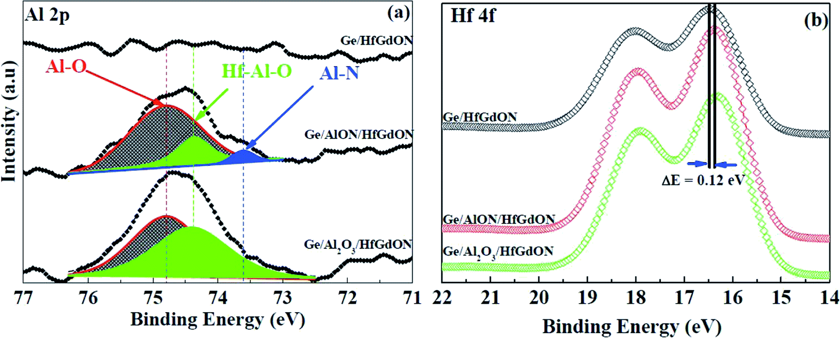 | ||
| Fig. 1 Al 2p (a) and O 1s (b) core level spectra of HfGdON/Ge gate stacks with different passivation layers. | ||
To further confirm the evolution of the interfacial chemical bonding states, much attention was paid to the Ge 3d and O 1s XPS spectra of HfGdON/Ge gate stacks with different passivation layers. In Fig. 2a, the two peaks located at the lower binding energies are attributed to the Ge substrate and the third one centered at 32.0 eV can be assigned to the GeON component.17 However, for the Ge/HfGdON gate stack without a passivation layer, a new peak at 32.50 eV was observed, which is due to the Ge–O bond states, indicating that a GeO2 interfacial layer is formed between the HfGdON sample and the Ge substrate.17,18 After applying the AlON passivation layer, the intensity of the Ge–O bond decreases, indicating that the GeO2 interfacial layer can be partly suppressed. It should be noted that no deleterious Ge–O bonding is detected for the sample with the Al2O3 passivation layer. The full removal of the GeO2 interfacial component can be attributed to the ALD-derived Al2O3 passivation layer with self-cleaning effect. A similar phenomenon has been observed in our previous work.19 Fig. 2b shows the O 1s core-level spectra of the HfGdON/Ge gate stack with different passivation layers. For the sample without a passivation layer, the four fitted peaks, located at binding energies of 529.7, 531.0, 531.9 and 532.4 eV, originate from the O–Hf, O–Gd, GeON and GeO2 bonding states, respectively.18,20 When inserting Al2O3 and AlON as a passivation layer, peaks located at 530.8 and 531.1 eV appear, which can be assigned to Hf–Al–O and O–Al (Gd). However, it is difficult to distinguish between the O–Gd and O–Al bonds, due to their similar binding energies (531.0 eV for Gd–O and 531.2 eV for Al–O).21 The peak located at 532.4 eV disappears when the Al2O3 passivation layer is applied, indicating that the GeO2 interfacial layer is effectively suppressed, which is in good agreement with previous Ge 3d spectra. As a result, it can be inferred that the HfGdON/Al2O3/Ge gate stack demonstrated optimized interface chemistry, and excellent CMOS device performance is expected.
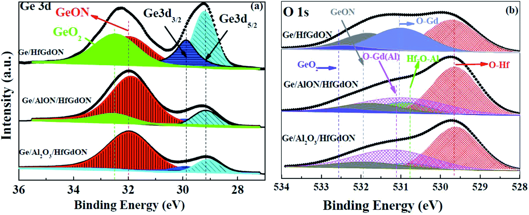 | ||
| Fig. 2 Ge 3d (a) and O 1s (b) core level spectra of HfGdON/Ge gate stacks with different passivation layers. | ||
In the application of high-k gate dielectrics to CMOS devices, the precise determination of the band offset (BO) is a major concern. It is critical to the success of a MOSFET containing a high-k gate dielectric that the BO between the high-k gate dielectric and the semiconductor is at least 1 eV. Based on the method proposed by Kraut et al.,22 the valence band alignment (ΔEv) of HfGdON/Ge gate stacks with different passivation layers could be determined by measuring the VB maximum (EVBM) difference between the high-k stacks and the Ge substrate, as expressed by the following equation:
| ΔEv = EstackVBM − EGeVBM | (1) |
The ΔEv values for the HfGdON/Ge heterojunctions with different passivation layers, shown in Fig. 3a, are calculated to be 0.86, 1.33 and 1.25 eV. The conduction band offset (ΔEc) was obtained simply subtracting the valence band offset and the energy gap of the Ge substrate and HfGdON film. Taking into account the measured energy band gap of sputtering-deposited HfGdON (5.64 eV), together with the Ge energy band gap of 0.59 eV, ΔEc of 3.72 eV was deduced for the AlON passivation layer, whereas 3.80 eV was obtained for the Al2O3 passivation layer, as demonstrated in Fig. 3b. An increase in ΔEc was detected after Al2O3 passivation, which can be attributed to reduction in the interfacial layer. Based on Fig. 3b, it can be seen that the ΔEv of the HfGdON/Ge gate stack without the passivation layer is only 0.86 eV, which cannot meet the primary requirements of high-k dielectrics. After inserting passivation layers, an increase in ΔEv and ΔEc was observed, which makes the HfGdON/Ge gate stacks with a passivation layer suitable for the fabrication of MOSFETs with a small leakage current induced by Schottky emission.23
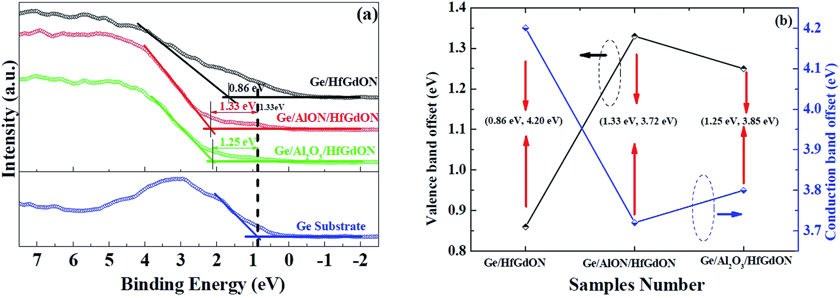 | ||
| Fig. 3 (a) Valence-band spectra of the Ge substrate and HfGdON/Ge gate stacks with different passivation layers. (b) Determination of band offsets for HfGdON/Ge gate stacks with different passivation layers. | ||
Fig. 4a shows the typical high frequency (1 MHz) C–V characteristics of Ge MOS capacitors with and without a passivation layer. For the sample without passivation treatment, the existence of a relatively large hysteresis can be attributed to the active defects near the interface or in the bulk HfGdON film.24 After passivation, negligible hysteresis was detected, implying improved interface quality and decreased interface state density in the dielectric and near or at the interface due to the reduced interface layer.25 Suppressed low-k layer formation was thus achieved, which results in high accumulation capacitance compared to directly deposited HfGdON. In addition, the extracted positive flat band voltage (VFB) indicates that the native defects/traps in the samples are negative. In contrast with the HfGdON/Ge and HfGdON/AlON/Ge samples, VFB for the HfGdON/Al2O3/Ge gate stack shifts towards the negative direction and displays a smaller positive value, indicating the less negative trapped charges, which can be attributed to the reduced defect traps in the film and near the interface.24 The effective dielectric constant (k), EOT, VFB, hysteresis (ΔVFB), and border trapped oxide charge density (Nbt) were extracted from the C–V curves and are listed in Table 1. Due to the suppressed growth of the low-k interfacial layer, HfGdON/Al2O3/Ge achieves the larger k value of 35.70. For Nbt, reduction was observed after passivation. As a result, it can be concluded that the presence of the Al2O3 passivation layer helps the formation of a high-quality interface between HfGdON and Ge by reducing interface states and border traps and thus unpinning the Fermi level. Fig. 4b shows the current density–voltage (J–V) characteristics for samples with and without a passivation layer. The larger leakage current for the HfGdON/Ge sample may originate from the interface trap-assisted tunneling, because a high density of interface states exists at the high-k/Ge interface of the unpassivated samples.24 Suppression of the gate leakage current by applying an Al2O3 passivation layer was clearly observed, which can be attributed to the suppressed interfacial layer growth, reduced oxygen-vacancy-related interface states, or the increased conduction band offset, leading to the reduced trap-assisted tunneling current.
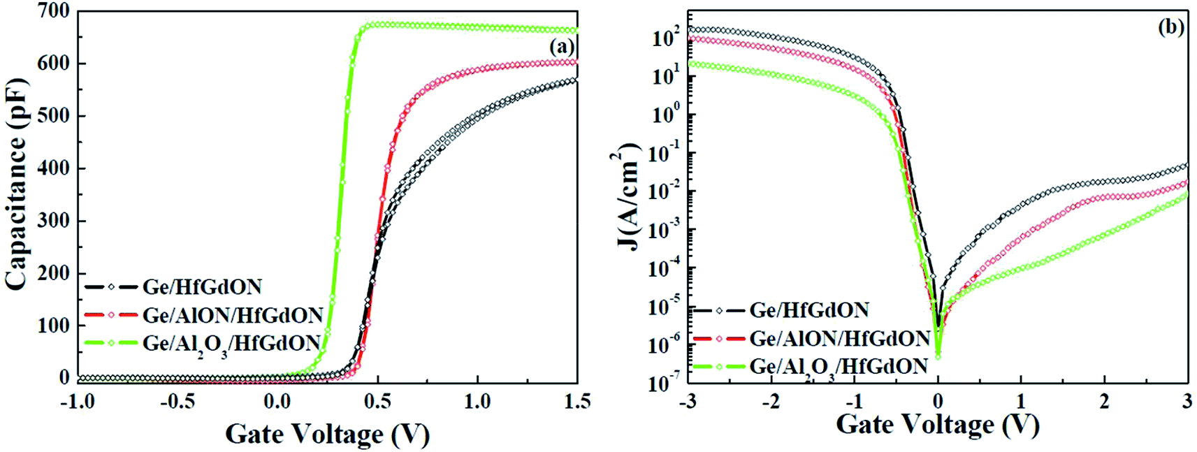 | ||
| Fig. 4 C–V and J–V characteristics of Ge-based MOS capacitors with different passivation layers. | ||
| Samples | k | EOT (nm) | VFB (V) | ΔVFB (V) | Nbt (cm−2) |
|---|---|---|---|---|---|
| HfGdON/Ge | 28.65 | 1.91 | 0.42 | 0.013 | 1.47 × 10¹¹ |
| HfGdON/AlON/Ge | 32.50 | 1.80 | 0.43 | 0.004 | 4.77 × 10¹⁰ |
| HfGdON/Al2O3/Ge | 35.70 | 1.64 | 0.24 | 0.001 | 1.32 × 10¹⁰ |
To investigate the current conduction mechanisms (CCMs) of the Ge-based MOS capacitors with and without a passivation layer, several CCMs including Fowler–Nordheim (FN) tunneling, Schottky emission (SE), and Frenkel–Poole (PF) emission were explored. As we know, various CCMs occur in various electric fields, so it is complicated to determine the exact CCM. In the current work, CCMs were only evaluated under substrate injection.
SE is carrier transportation induced by thermionic emission, in which electrons obtain enough energy after thermal excitation to pass through the metal–dielectric barrier or the dielectric–semiconductor barrier to the dielectric. Based on the SE mechanism,19 if SE is the dominant mechanism, ln(J/T2) versus the E1/2 should satisfy a linear relationship. Fig. 5a shows the good linear behavior of ln(J/T2) vs. E1/2, indicating that the dominant CCM is SE under substrate injection in a low electric field of 0.16–0.64 MV cm−1. Based on the linear fitting, the optical dielectric constant εr and the refractive index n have been calculated to be (5.78, 2.40), (3.86, 1.96) and (5.07, 2.25) for substrate injection, corresponding to HfGdON/Ge, HfGdON/AlON/Ge and HfGdON/Al2O3/Ge, respectively. All the obtained εr and n values are in good agreement with the reported results, suggesting that the SE emission dominates the CCM under substrate injection in a low electric field.26,27 Fig. 5b–d present ln(J/E) vs. E1/2 of the three samples for the substrate injection at room temperature. According to the theoretical expressions for the PF mechanism,28 ln(J/E) should be proportional to E1/2. From the slope of the linear plots, the values of the dielectric constant of the HfGdON films (εox) are determined to be 18.9, 31, and 58.85 for the unpassivated, Al2O3-passivated, and AlON-passivated samples, respectively. It should be noted that the εox value of 58.85 is far from being a reasonable value for the AlON-processed sample. As a result, it can be concluded that the PF emission is the dominant CCM for the unpassivated and Al2O3-passivated samples in a medium-strength electric field, whereas this is not the case for the AlON-passivated sample. Normally, in the high electric field regions, the dominant CCM is governed by FN tunneling, which follows the linear relation of ln(J/E2) versus 1/E.25 Fig. 5e displays ln(J/E2) vs. 1/E for the three samples at high field regions. The linear relation of ln(J/E2) vs. 1/E indicates FN tunneling through the HfGdON oxide layer under substrate injection under a high electric field of 1–1.67 MV cm−1 at room temperature. According to the previous analysis, it can be concluded that with the increases of the electric field, the dominant CCM change is from SE to FN tunneling and/or PF emission.
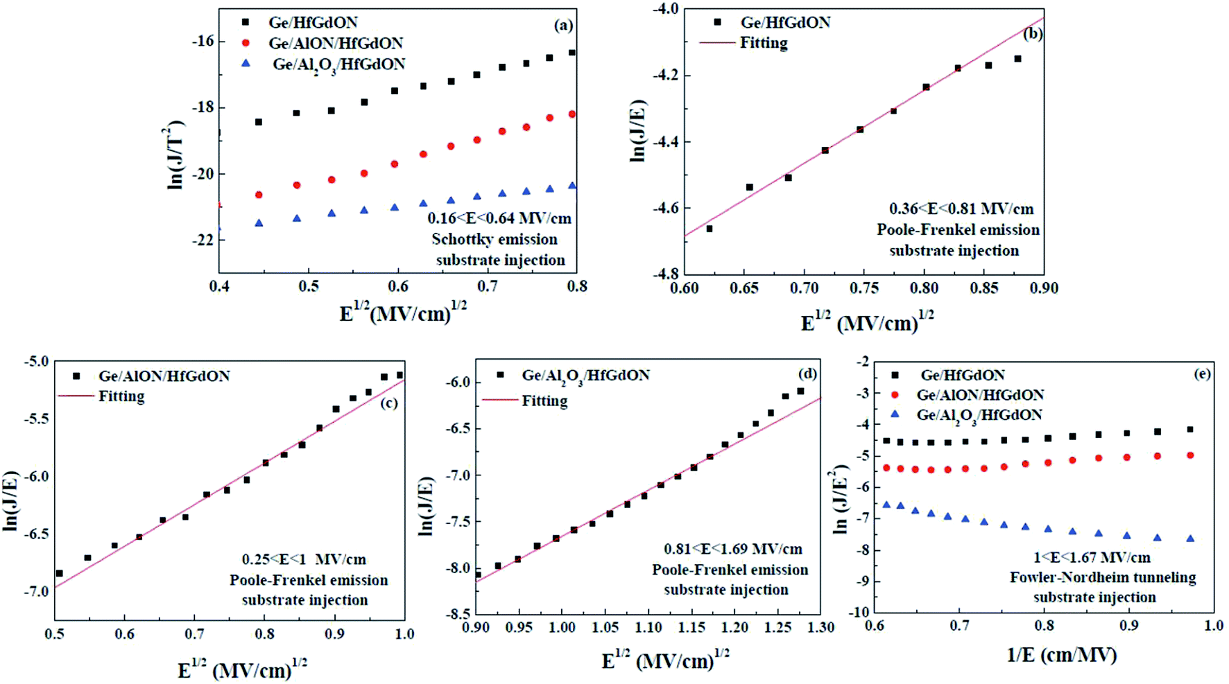 | ||
| Fig. 5 (a) SE, (b–d) PF emission, and (e) FN tunneling plots for Ge-based MOS capacitor with different passivation layers under substrate injection at room temperature. | ||
4. Conclusion
In this work, the effects of an ALD-driven passivation interlayer on the interfacial defect states and electrical properties of Ge-based MOS capacitors with a HfGdON gate dielectric have been investigated. Electrical measurements confirm that the HfGdON/Al2O3/Ge MOS device demonstrates improved performance, including the largest dielectric constant of 35.70, negligible hysteresis, and lower interface state density and border trapped oxide charge density. XPS investigations reveal that the ALD-derived Al2O3 interlayer with self-cleaning effect can effectively suppress the formation of unstable native oxides, and also reduce the oxide traps at and near the high-k/Ge interface, thus leading to the excellent electrical performance for the Ge-based MOS device. The CCM analyses, including SEs, PF emissions and FN tunneling, measured at room temperature, were discussed systematically. As a result, it can be inferred that the ALD-driven Al2O3 interlayer possesses optimized interface chemistry and improved electrical performance, highlighting its potential as a promising passivation candidate for the next generation of Ge-based MOSFET devices.Conflicts of interest
The authors declare no competing financial interest.Acknowledgements
This work is financially supported by the National Natural Science Foundation of China (11774001, 51572002), Open Fund for Discipline Construction, Institute of Physical Science and Information Technology, Anhui University (S01003101).References
- Y. Huang, J. P. Xu, L. Liu, Z. X. Cheng, P. T. Lai and W. M. Tang, Appl. Phys. Lett., 2017, 111, 053501 CrossRef.
- Z. X. Cheng, J. P. Xu, L. Liu, Y. Huang, P. T. Lai and W. M. Tang, Appl. Phys. Lett., 2016, 109, 023514 CrossRef.
- F. Ji, J. P. Xu, J. G. Liu, C. X. Li and P. T. Lai, Appl. Phys. Lett., 2011, 98, 182901 CrossRef.
- Y. Huang, J. P. Xu, L. Liu, P. T. Lai and W. M. Tang, Appl. Phys. Lett., 2017, 109, 193504 CrossRef.
- Y. Fukuda, H. Okamoto, T. Iwasaki, Y. Otani and T. Ono, Appl. Phys. Lett., 2011, 99, 132907 CrossRef.
- T. J. Seok, Y. J. Cho, H. S. Jin, D. H. Kim, D. W. Kim, S. M. Lee, J. B. Park, J. Y. Won, S. K. Kim, C. S. Hwang and T. J. Park, J. Mater. Chem. C, 2016, 4, 850 RSC.
- R. L. Chu, Y. C. Liu, W. C. Lee, T. D. Lin, M. L. Huang, T. W. Pi, J. Kwo and M. Hong, Appl. Phys. Lett., 2014, 104, 202102 CrossRef.
- D. Kuzum, T. Krishnamohan, A. J. Pethe, A. K. Okyay, Y. Oshima, Y. Sun, J. P. McVittie, P. A. Pianetta, P. C. McIntyre and K. C. Saraswat, IEEE Electron Device Lett., 2008, 29, 328 CAS.
- Y. J. Choi, H. Lim, S. Lee, S. Suh, J. R. Kim, H.-S. Jung, S. Park, J. H. Lee, S. G. Kim and C. S. Hwang, ACS Appl. Mater. Interfaces, 2014, 6, 7885 CrossRef CAS.
- G. Mavrou, S. Galata, A. Sotiropoulos, P. Tsipas, Y. Panayiotatos, A. Dimoulas, E. Evangelou, J. W. Seo and C. Dieker, Microelectron. Eng., 2007, 84, 2324 CrossRef CAS.
- Q. Xie, S. R. Deng, M. Schaekers, D. Lin, M. Caymax, A. Delabie, X. P. Qu, Y. L. Jiang, D. Deduysche and C. Detavernier, Semicond. Sci. Technol., 2012, 27, 074012 CrossRef.
- J. Gao, G. He, D. Q. Xiao, S. S. Jiang, J. G. Lv, C. Cheng and Z. Q. Sun, Mater. Res. Bull., 2017, 91, 166 CrossRef CAS.
- J. Gao, G. He, D. Q. Xiao, P. Jin, S. S. Jiang, W. D. Li, S. Liang and L. Zhu, J. Mater. Sci. Technol., 2017, 33, 901 CrossRef.
- R. Ma, M. Liu, G. He, M. Fang, G. L. Shang, G. T. Fei and L. D. Zhang, J. Appl. Phys., 2016, 119, 214103 CrossRef.
- R. Suri, C. J. Kirkpatrick, D. J. Lichtenwalner and V. Misra, Appl. Phys. Lett., 2010, 96, 042903 CrossRef.
- G. He, Z. Q. Sun, M. Liu and L. D. Zhang, Appl. Phys. Lett., 2010, 97, 192902 CrossRef.
- Y. Oshima, M. Shandalov, Y. Sun, P. Pianetta and P. Mclctyre, Appl. Phys. Lett., 2009, 94, 183102 CrossRef.
- P. Mclctyre, Y. Oshima, E. Kim and K. Saraswat, Microelectron. Eng., 2009, 86, 1536 CrossRef.
- J. Gao, G. He, S. Liang, D. Wang and B. Yang, J. Mater. Chem. C, 2018, 6, 2546 RSC.
- M. Liu, L. D. Zhang, G. He, X. J. Wang and M. Fang, J. Appl. Phys., 2010, 108, 024102 CrossRef.
- L. Y. Huang, A. D. Li, Y. Y. Fu, W. Q. Zhang, X. J. Liu and D. Wu, Microelectron. Eng., 2012, 94, 38 CrossRef CAS.
- E. A. Kraut, R. W. Grant, J. R. Waldrop and S. P. Kowalczyk, Phys. Rev. Lett., 1980, 44, 1620 CrossRef CAS.
- J. W. Liu, M. Y. Liao, M. Imura and Y. Koide, Appl. Phys. Lett., 2012, 101, 252108 CrossRef.
- H. S. Jung, I. H. Yu, H. K. Kim, S. Y. Lee, J. Lee, Y. Choi, Y. J. Chung, N. Lee, T. J. Park, J. Choi and C. S. Hwang, IEEE Trans. Electron Devices, 2012, 59, 2350 CAS.
- G. He, J. Gao, H. S. Chen, J. B. Cui, X. S. Chen and Z. Q. Sun, ACS Appl. Mater. Interfaces, 2014, 6, 22013 CrossRef CAS.
- R. Ma, M. Liu, G. He, M. Fang, G. L. Shang, J. W. Zhang, X. F. Chen, J. Gao, G. T. Fei and L. D. Zhang, J. Alloys Compd., 2015, 646, 310 CrossRef CAS.
- Y. H. Xiong, H. L. Tu, J. Du, L. G. Wang, F. Wei, X. Q. Chen, M. M. Yang, H. B. Zhao, D. P. Chen and W. W. Wang, Phys. Status Solidi B, 2014, 251, 1635 CrossRef CAS.
- R. P. Ortiz, A. Facchetti and T. J. Marks, Chem. Rev., 2010, 110, 205 CrossRef CAS.
| This journal is © The Royal Society of Chemistry 2019 |