
 Open Access Article
 This Open Access Article is licensed under a Creative Commons Attribution-Non Commercial 3.0 Unported Licence
Highly transparent copper iodide thin film thermoelectric generator on a flexible substrate
J. Coroa a,
B. M. Morais Faustino*a,
A. Marquesa,
C. Bianchia,
T. Koskinenb,
T. Juntunenb,
I. Tittonenb and
I. Ferreiraa
a,
B. M. Morais Faustino*a,
A. Marquesa,
C. Bianchia,
T. Koskinenb,
T. Juntunenb,
I. Tittonenb and
I. Ferreiraa
aCENIMAT/I3N, Departamento de Ciência dos Materiais, Faculdade de Ciências e Tecnologia, Universidade Nova de Lisboa, Caparica, 2829-516, Portugal. E-mail: bm.faustino@fct.unl.pt
bDepartment of Electronics and Nanoengineering, Aalto University, P.O. Box 13500, FI-00076, Aalto, Finland
First published on 1st November 2019
Abstract
Simultaneously transparent and flexible conductive materials are in demand to follow the current trend in flexible technology. The search for materials with compliant optoelectronic properties, while simultaneously retaining their electric conductivity at high strain deformation, comprises promising opportunities in modern nanotechnology. Copper iodide (CuI) is not only the most transparent and highly conductive p-type material, but its optimization has contributed to improved ZT values in planar thin-film thermoelectrics. In this work, the readiness of CuI thin films to transparent, flexible technology is evidenced. A maximum ZT value of 0.29 for single CuI thin films of ca. 300 nm in thickness is reported. Values of open-circuit voltage Voc, short circuit current Isc and power output of p–n thermoelectric modules of Gallium-doped zinc oxide (GZO) and CuI thin films deposited on a transparent flexible Kapton® (type CS) substrate are reported, and a prototype of a flexible transparent thermoelectric generator based on 17 p–n modules was constructed. Bending analysis of CuI thin films reveals interesting, distinct results when submitted to compression and tension analysis – a behaviour not seen in conventional semiconducting thin films under equivalent strain conditions. A plausible account for such diversity is also included.
1. Introduction
Transparent conducting oxides (TCO) have been vastly studied and applied to transparent technology. Most of the currently-in-market TCOs are n-type semiconductors, such as SnO2 and ZnO based thin films. However, as most of the semiconductor applications rely on p–n junctions (e.g. diodes, lasers, etc.), p-type semiconductors with equivalent performance are required. In general, p-type transparent conductive oxides are not simultaneously electrically conductive and transparent to enable, for instance, bipolar devices with high electrical conductivities.1 In the field of thermoelectricity, transparent p-type thermoelectric (TE) materials exhibit poor electric conductivity – often several orders of magnitudes lower than n-type TE materials. This is the case for thin films of CuAlO2 (ref. 2 and 3) and CuCrO2 (ref. 4) transparent p-type materials with TE potential and with ZT values in the order of 1 × 10⁻³. Copper iodide (CuI) thin films have been of recent interest in the field of planar TE thin films. CuI is to date the most efficient TE material that is simultaneously both transparent and conductive. A preliminary study on the growth of CuI thin films revealed that physical vapour deposition (PVD) technique is an efficient process towards the production of planar, transparent TE thin films with ZT values of up to 0.22.5 This significant improvement maximises the TE efficiency of wide-gap non-oxide p-type materials. Thermoelectric performance largely depends on the electronic composition near the valence band maximum of any material. The fact that a maximum Seebeck coefficient of 250 μV K−1 and a hole concentration up to 1020 cm−3 can be theoretically predicted based on first-principle calculations,6 means that currently studies no longer focus on the novelty of the CuI material, but rather on applying it to current technology. Whether applied to rectification layers in solar cells7 or in p–n thermoelectric modules,5 the current trend in transparent technology is towards materials that are simultaneously transparent in the visible range of the spectrum and offer some degree of bending flexibility.8,9 In this study, the first highly transparent and flexible p–n thermoelectric generator (TEG) of 17 p–n modules electrically connected in series and thermally in parallel was successfully constructed and tested at temperature gradients of up to 30 °C.2. Experimental
Copper thin films were fabricated by resistive thermal evaporation under vacuum at a rate of 0.1 nm s−1 to reach an average Cu thickness of 60 nm onto Kapton (type CS) flexible substrates of 50 μm thick – a polyimide transparent substrate as supplied by Dupont™.Afterwards, the iodination of Cu thin films was performed according to optimal conditions determined in a previous study.5 The iodination occurred in a sealed box purged with N2 prior to and post the addition of solid iodine (purity 99.9% supplied by Sigma Aldrich®) on top of Cu thin films for a period of 60 min to yield a transparent γ-CuI thin film:
| 2Cu + I2(s) → 2CuI |
To maximise the TEG power output, several p- and n- TE modules were electrically connected in series and thermally in parallel through transparent indium tin oxide (ITO) conductive electrodes. The TE modules were fabricated with masks applied to a 10 × 10 cm2 transparent flexible Kapton® substrate, used as received from DuPont™. The process required the use of 2 masks with multiple 1 × 1 cm2 square holes, carefully designed to allow the alternating deposition of p–n elements. Gallium doped zinc oxide (ca. 300 nm thick) was chosen as the n-type counterpart and this was deposited by RF magnetron sputtering using a GZO (ZnO![[thin space (1/6-em)]](https://www.rsc.org/images/entities/char_2009.gif) :Ga 95:5) target supplied by Plasmaterials for a period of 60 min using an RF power in the range of 100–150W and a working pressure between 1.2–2.0 mTorr. Conductive electrodes of indium tin oxide (ITO, ca. 300 nm thick) were also sputtered and provided 80 Ω. The ITO sputtering targets were supplied by Super Conductor Materials Inc.
:Ga 95:5) target supplied by Plasmaterials for a period of 60 min using an RF power in the range of 100–150W and a working pressure between 1.2–2.0 mTorr. Conductive electrodes of indium tin oxide (ITO, ca. 300 nm thick) were also sputtered and provided 80 Ω. The ITO sputtering targets were supplied by Super Conductor Materials Inc.
TEG bending properties and stability were studied over repeated bending cycles using a home-build setup (Fig. 1) with in situ resistance measurement as a function of the bending radius. These profiles acquired to each cycle were performed according to a widely referenced method10 which delivered the calculus of the critical bending radius for each cycle. This is defined as the bending curvature radius at which the resistance exceeds 5% or 10% of its original value. Generally, the setup consists of two grips, whereas one is attached to a non-movable arm holding the sample at one end of the substrate, and the other one is attached at a stage that moves back and forth with an accuracy and minimal step increment of ∼0.01 mm. Fig. 1 shows the substrate at the initial length L, bent to an end-to-end length of L − dL and the bending radius r at the centre of the sample, computed using eqn (1). The initial length of the sample and rate of change of the length are denoted by L and dL/L, and h is the sum of the substrate thickness, ts, and the film thickness, tf.
 | (1) |
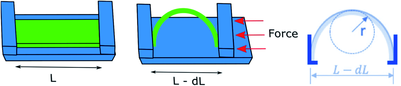 | ||
| Fig. 1 Schematics of the home made bending machine and the consequent bending radius r determined for each displacement L − dL. The resistance of the sample is measured through two conductive wires that are connected to the sample ends. | ||
3. Results and discussion
Optoelectronic and thermoelectric properties were investigated in CuI and GZO elements individually prior to their application into p–n thermoelectric modules. The properties of CuI and GZO films deposited on flexible Kapton CS® substrates were also tested with respect to changes in electrical conductivities during bending.3.1. Transparency of CuI and GZO
Copper iodide is a wide band semiconductor with very high transmittance in the visible range of the spectrum (>70%) and with significant absorption at the direct band gap (ca. 3 eV), where free excitons recombine, and copper vacancy defects dominantly contribute to the band transport. A characteristic split-off band is seen at 0.6 eV above the valence band. Such an acceptor level enhances mobility by providing electron–hole delocalization at the top of the valence band.11 Similarly, gallium-doped zinc oxide thin films are extremely transparent in the visible range (>80% transmittance) owing to its wide-gap. Fig. 2 reveals the transmittance of both GZO and CuI thin film on Kapton CS substrate using UV-VIS absorption spectroscopy.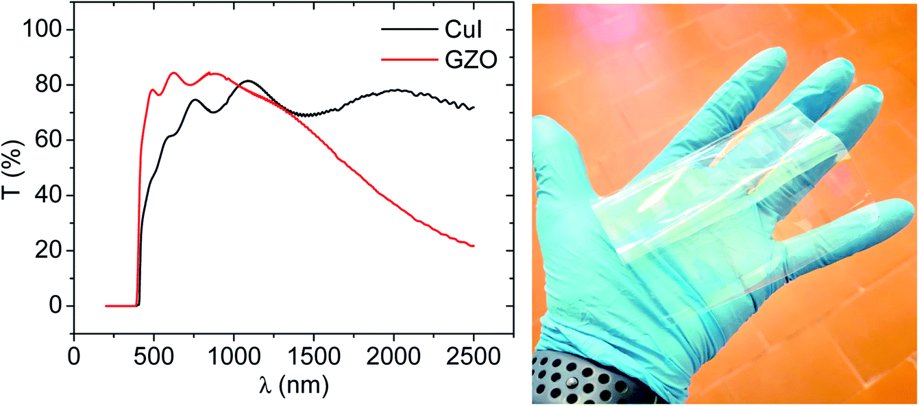 | ||
| Fig. 2 Transmittance spectra of CuI and GZO thin films on Kapton CS® substrate (Left); A 10 × 10 cm2 Kapton based prototype with alternating p–n type modules of CuI and GZO, interconnected electrically in series with ITO. | ||
3.2. Thermoelectric properties of CuI and GZO
Table 1 summarizes the thermoelectric efficiency of both p-type CuI and n-type GZO films. The effect of the iodination process and iodine exposure time on the electrical conductivity of CuI has been extensively investigated in our previous study.5 Note that, although the Seebeck coefficient of GZO is significantly lower than that of CuI, its electrical conductivity is of one order of magnitude higher than that of CuI, which leads to similar power factors. The thermal conductivity of CuI and GZO are 0.48 and 2.17 W (m2 K)−1, respectively. As a result, the ZT values of CuI and GZO are 0.29 and 0.07, respectively.| Material | Thickness (nm) | Conductivity (Ω−1m−1) | Seebeck (μV K−1) | Power factor (W m−1 K−2) | Charge carrier density (×1020 cm−3) | Hall mobility (cm2 V−1 s−1) | Thermal conductivity (W m−2 K−1) |
|---|---|---|---|---|---|---|---|
| p-type CuI | 302 | 1.1 × 10⁴ | 206.0 | 4.7 × 10⁻⁴ | 1.7 | 4.1 | 0.48 |
| n-type GZO | 306 | 1.42 × 10⁵ | −60 | 5 × 10⁻⁴ | 5.9 | 15 | 2.17 |
3.3. The flexibility of γ-CuI and GZO on Kapton CS
The bending flexibility of each semiconducting film deposited on Kapton CS substrate was separately characterized through compressive and tensile strength analysis. As illustrated in Fig. 3, the type of force applied to the thin film (compressive or tension) depends on which side of the substrate the film is deposited on. Along with the critical bending radius, that is a direct measure of the maximum radius of the bending curvature before irreversible film destruction, Fig. 4 demonstrates that the type of force applied to the film during bending is also critical in defining electrical stability.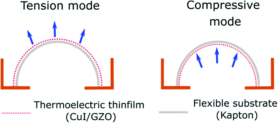 | ||
| Fig. 3 Tension and compressive forces applied to the thin film on a flexible Kapton substrate during bending analysis. | ||
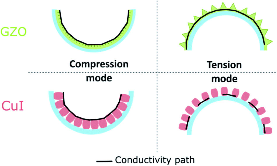 | ||
| Fig. 4 Conductivity path for GZO and CuI in tension and compression mode. | ||
A complete bending cycle involves the bending and releasing of the sample, where values of the initial (R0) and final (Rf) resistance are noted after each cycle. As previously described, the critical bending radius is defined as the curvature at which the internal film resistance (Rint) exceeds 5% or 10% of its original value. As such, it is only reasonable to comment on values of critical bending radius for samples exposed to tension forces. In this case, after the first bending cycle under tension, CuI has kept a resistance variation below 10% but with a critical bending radius of 15.5 mm assessed at values of film resistance exceeding 5% of R0. During compression mode, the resistance variation was always below 5%. Hence, in subsequent cycling tests, aiming at assessing the semiconducting films performance reliability under continuous bending, the bending radius was varied out of the critical range to values of up to 18.6 mm. Fig. 5A shows that over 100 cycles, the compressive force applied is producing an electrical resistance variation of less than 5% of the initial resistance of the film. However, Fig. 5B shows that CuI thin films subjected to a tensile force result in the electrical resistance being linearly degraded with the number of bending cycles up to 80 cycles, beyond which a plateau of change in R seems to be established. A total of 100 bending cycles produces an average variation of 9% of the initial resistance R0. However, as also shown in Fig. 5B, when CuI is subjected to compressive forces, a maximum of 3.6% of R0 is observed with 100 full bending cycles. This is explained by the imposed compressing forces on the columnar grains of CuI causing further compacting of the lattice which aids electron flow, whereas the opposite would further disrupt the lattice and ultimately results in film cracks preventing the flow of carriers. Exposing the film to compressive forces after 100 tension cycles results in a reduction of its internal resistance Rint by 7.1% with a single compressive cycle. A lower Rint value occurs after the 13th compression cycle to yield a resistance value of 0.4% change from its R0 before tension forces were applied; nonetheless, further compression produces a slight increase in Rint after 100 cycles. This is not the case for a film which did not previously undergo tension forces during the bending of the flexible substrate – Rint remains reasonably stable after 100 cycles, as demonstrated in Fig. 5A.
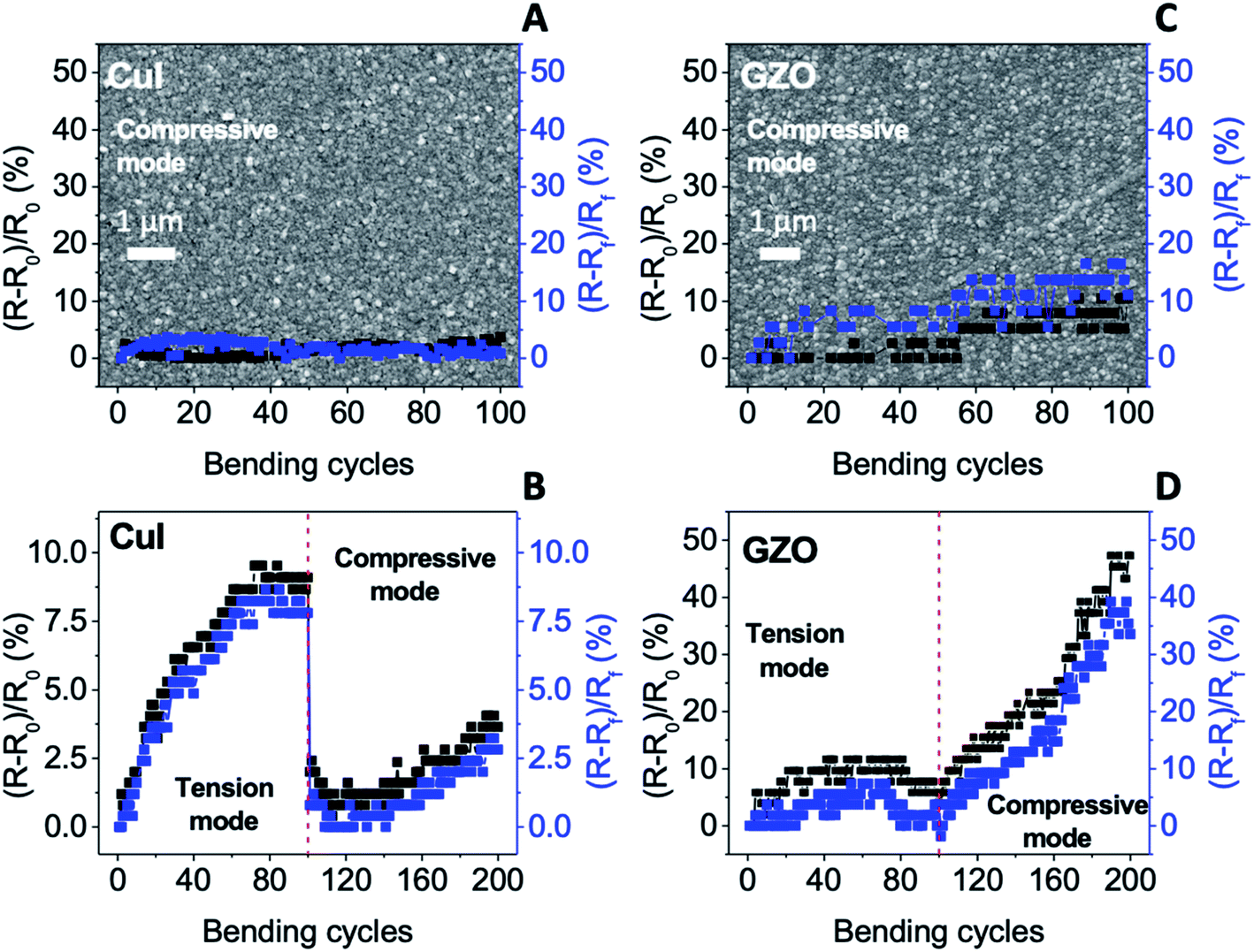 | ||
| Fig. 5 Bending properties of CuI and GZO thin films deposited on Kapton CS substrate. (A) 100 bending cycles of a single compressive mode of CuI and (C) of GZO (background – corresponding scanning electron micrograph after 100 consecutive cycles in compressive mode). (B) and (D)The effect of 100 cycles in compressive mode after 100 cycles in tension mode. | ||
In contrast to the behaviour of CuI, GZO thin films are of ceramic nature with a compact structure and thus showing a resistance variation less sensitive to tension than compression, as shown in Fig. 5C and D. During tension, an increase in resistance of GZO is attributed to the formation of rather superficial cracks in the film, but not deep enough to prevent the flow of carriers (Fig. 6B). However, posterior compression following tensile cycles will result in GZO film cracking in the opposite face of the thin film (in contact with substrate) and thus disturbing the remaining flow of carriers in depth (Fig. 6D). In some cases, GZO thin films which underwent consecutive tensile and compressive cycles revealed areas of an apparent film disintegration or pilling due to excessive cracking even if at a nanoscale.
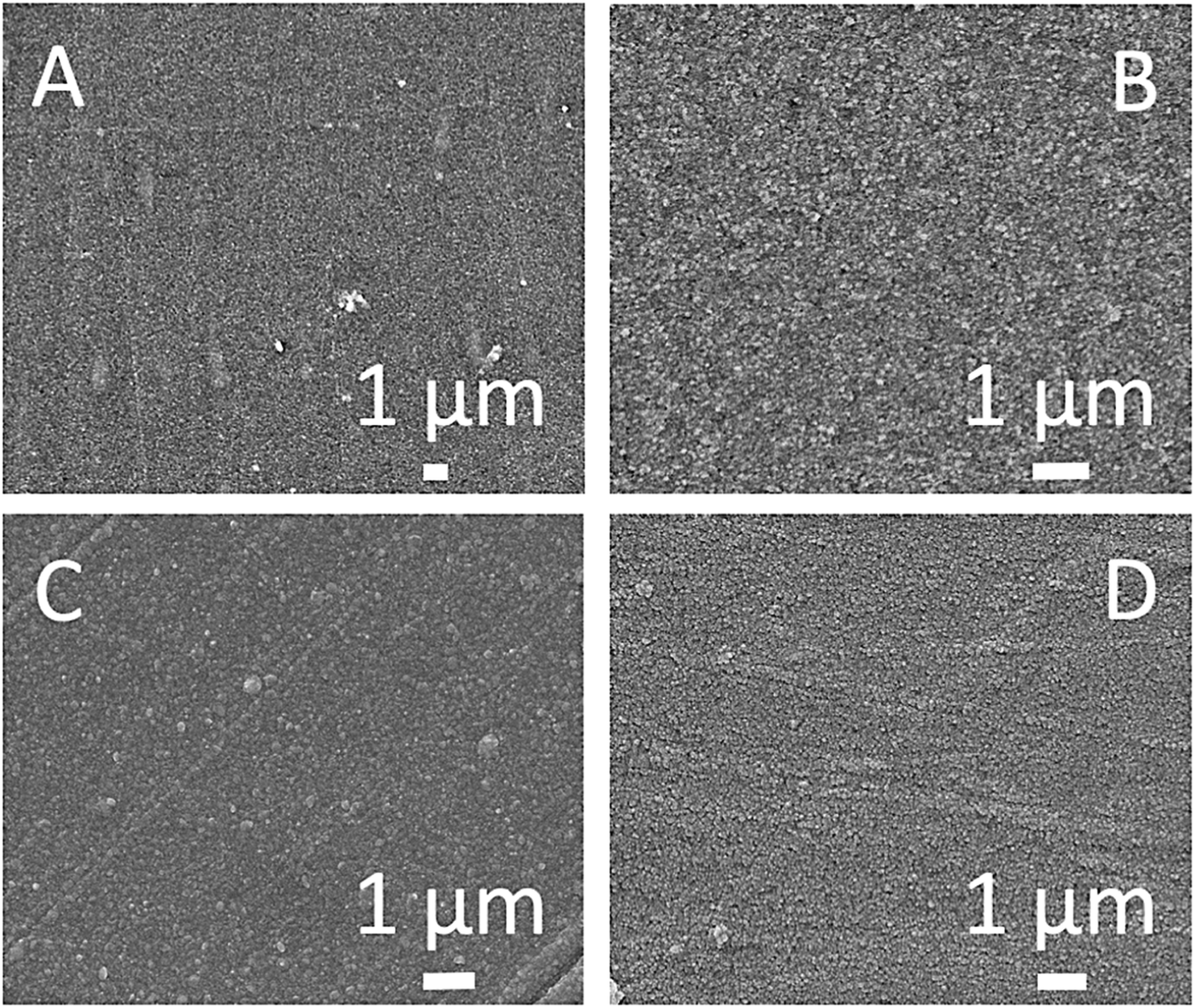 | ||
| Fig. 6 Scanning electron micrographs of CuI and GZO thin films. (A) CuI thin film on Kapton substrate after 100 tension bending cycles; (B) GZO thin film deposited on Kapton substrate after 100 tension bending cycles; (C) CuI thin film on Kapton substrate after 100 tension cycles plus 100 compression bending cycles; (D) GZO thin film on Kapton substrate after 100 tension cycles plus 100 compression bending cycles. | ||
Overall, the resistance variation over 100 bending cycles is minimal for CuI thin films deposited on transparent Kapton CS, irrespectively of the bending mode used, as it never exceeds 10%. This is a remarkable result.
3.4. A transparent and flexible thermoelectric generator
The construction of alternating p–n elements connected electrically in series and thermally in parallel increases the application versatility, such refrigeration via the Peltier effect – which requires a p–n module –, aside from generally benefitting from two different carrier types to maximise thermoelectric potential at the collection points.As illustrated in Fig. 7A, indium tin oxide electrodes are deposited at a 6 mm distance. Power output performances, current–voltage (I–V) and power–voltage (P–V) curves were recorded for pre-defined temperature gradients applied across its planar dimension as opposed to across thickness in bulk materials while varying load resistances. Those temperature gradients were established with a low-diameter ∼0.12 mm wire placed at the heat source located under the substrate and adjacent to the charge injection points (on the heated side) of the p–n module. Whilst closing the circuit at both extremities and applying a current, heat is generated in the conductive wire through the Joule heating effect. A fixed temperature gradient is obtained varying the current load. The gradient is measured with the aid of an IR FLIRA310 thermal camera in the front side of the substrate, i.e. the side of the coated TE modules as shown in the thermal map of Fig. 7B.
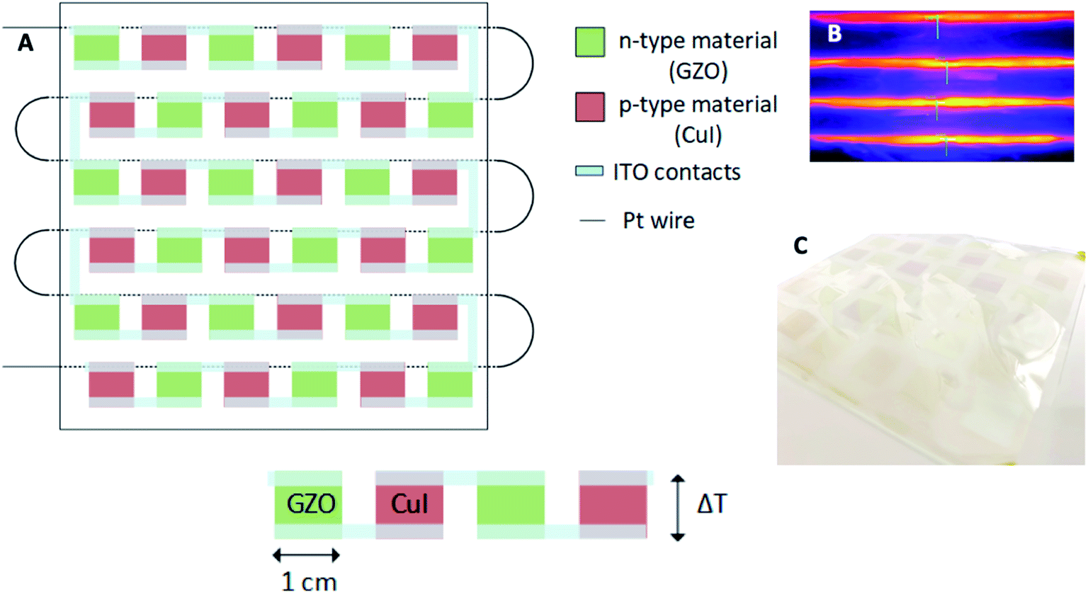 | ||
| Fig. 7 (A) Illustration of a flexible transparent thermoelectric generator with 17 p–n modules. (B) Mapping of the heat dissipation along-side the modules. The Pt wire is heating up the modules, thermally connecting them in parallel. (C) Final Prototype. | ||
In order to correctly assess the efficiency of such transparent and flexible TEG device, several configurations were tested by placing the nanovoltmeter probes at specific locations to access: single, double, triple, quadruple p–n modules, and at the total of 17 p–n modules electrically connected in series. In order to add-up contributions of each TE module, each probe is placed on the electrode at the same temperature (i.e. the potential measured is either by probing at the heat-sink or heated sides of the TEG, but never in opposing configurations).
Current–voltage (I–V) and power–voltage (P–V) characteristic curves were recorded as explained to each of the configurations mentioned above. Values of open-circuit voltage Voc, short circuit current Isc and the maximum output voltage Vout of single elements GZO and CuI increase linearly with increasing ΔT, as described by the generic equation:
| V = n(Sp − Sn) × ΔT − I × Rint | (2) |
The power output of the device is described by the following equation and adopts a non-linear dependency with ΔT:
| Pout = S × ΔT × I − I2×Rint | (3) |
At a ΔT of 5 °C, a single 1 × 1 cm2 GZO–CuI p–n module short circuit current Isc is of 0.29 μA and the maximum output voltage Vout is 0.43 mV. These values increase linearly with ΔT as described by the generic equation (eqn (2)) and observed in Fig. 8. Whilst varying load resistance, a maximum power output (Pout) of 0.51 nW is yielded at a current of 1.16 μA for a ΔT of 20 °C. The increase of power output with temperature follows (eqn (3)).
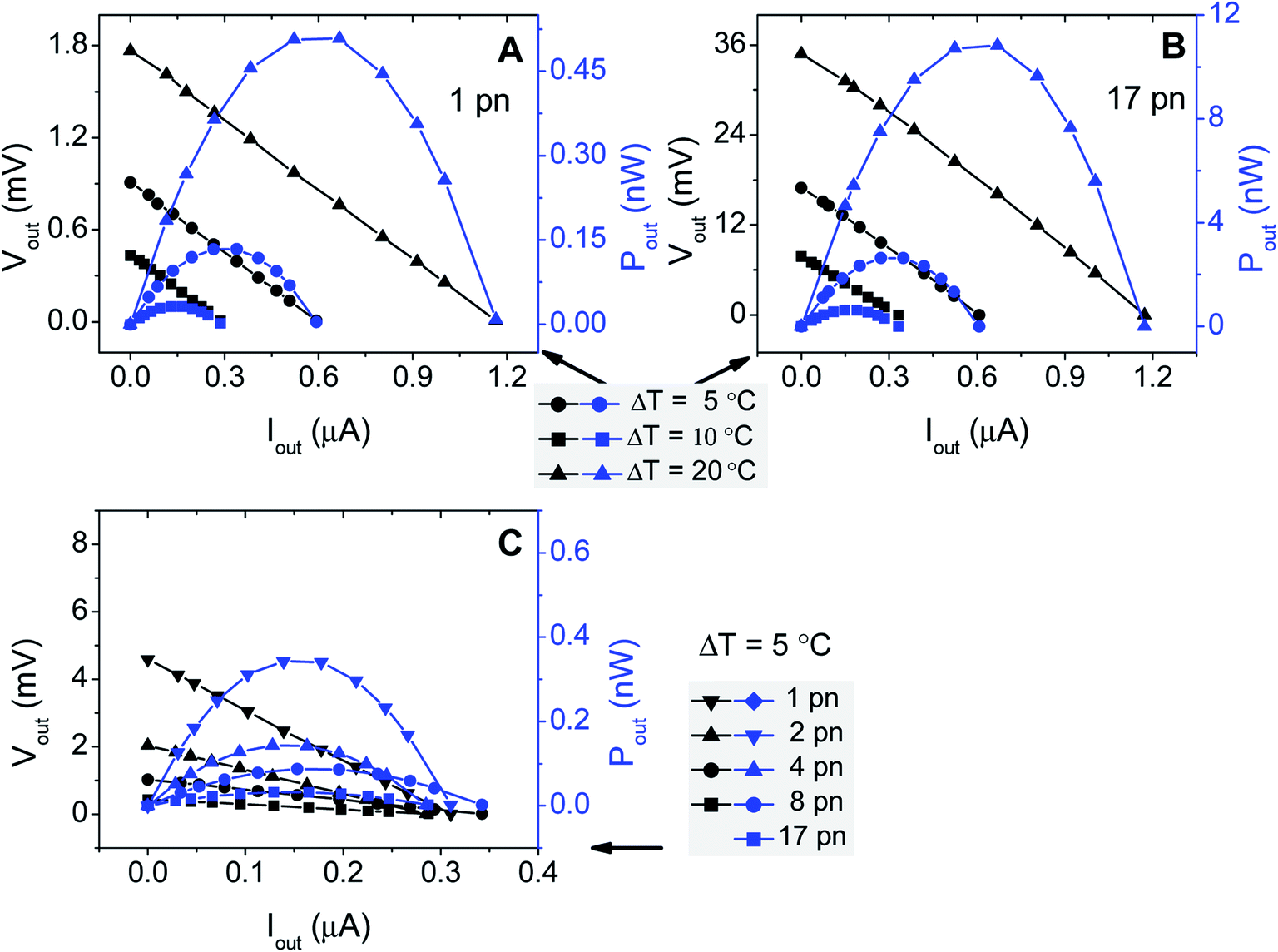 | ||
| Fig. 8 Current–voltage (I–V) and power–voltage (P–V) characteristic curves varying load resistance and temperature gradients for: (A) 1 p–n module (CuI/GZO); (B) 17 p–n modules electrically interconnected with ITO; and (C) All characterized p–n modules at a fixed gradient of 5 °C. | ||
Although a single p–n module may prove insufficient for the supply of low-power applications, multiple p–n modules electrically connected in series are certainly capable of reaching the milliwatt range of power density output. As demonstrated in Fig. 8, a total of 17 p–n modules are able to produce a maximum Pout value of 10.83 nW at 20 ΔT whilst keeping a relatively low Iout value. Nonetheless, interconnection resistance is indisputably a limiting factor on the operation of such prototypes, given the fact that CuI TE element Rint is already at the lowest conceivable as theoretically predicted6 based on the Boltzmann transport theory. As such, lowering Iout values require shortening the distance between ITO interconnections (e.g. by producing in-series-modules along with a more horizontal configuration, as opposed to vertically in series – as these require interconnecting always at the same temperature edge) is expected to influence Iout prominently.
To assess the electrical stability of CuI during heating, a sample of CuI was subjected to increasing temperatures whilst monitoring the change of Rint. Firstly, a cycle of increasing and decreasing temperature was applied (Fig. 9A) and later, a continuous increment of ΔT over time was also experimented (Fig. 9B).
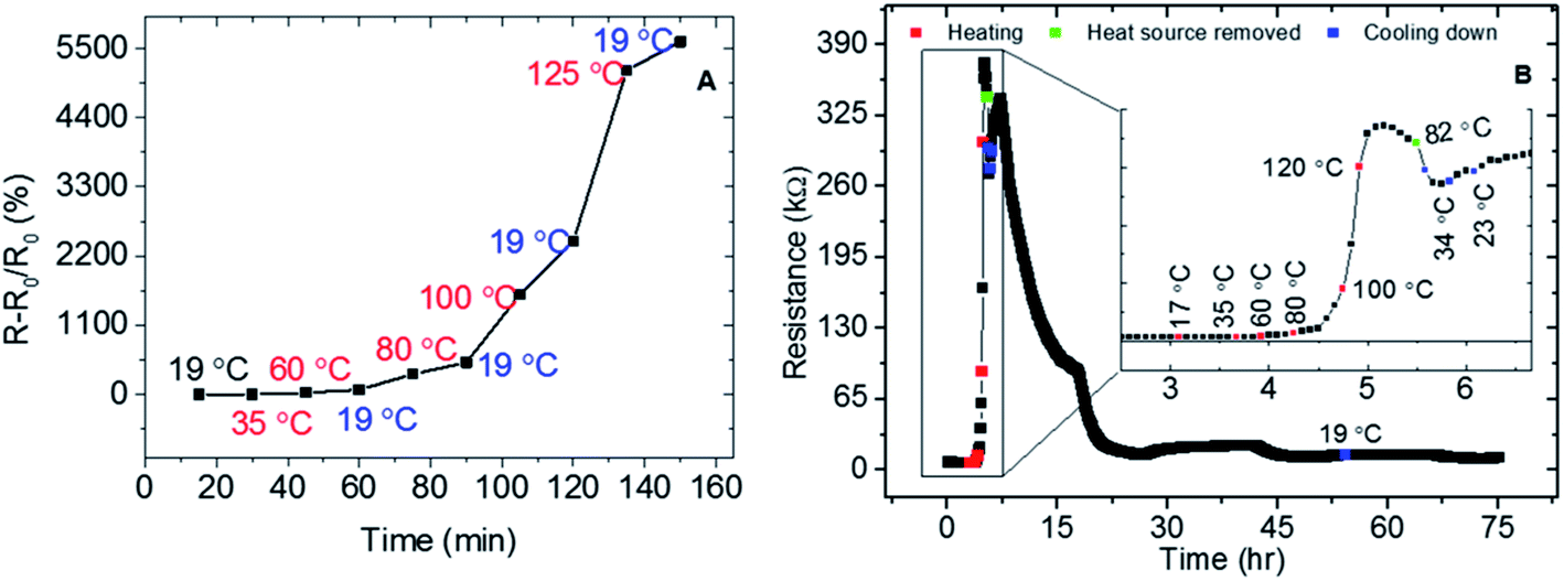 | ||
| Fig. 9 Change of internal resistance with increasing and decreasing temperature. (A) CuI is exposed to alternating heating a cooling processes at constant rate of heating/cooling; (B) CuI is exposed to constant heating up to 120 °C and then allowed to cool at room temperature. Different processes of resistance reversibility can be identified. | ||
CuI is stable in air up to 80 °C, beyond which Rint increases significantly and hinders its use in TE applications. A specific cooling time of 15 min was not enough to produce any reversibility in the process, but the rate of change of Rint was lower. Yang et al.9 found similar results where ZT values increased up to a temperature of 77 °C, beyond which a decrease in conductivity was similarly observed. However, the authors justify this change in conductivity based on iodide diffusion. Yamada et al.,7 observed simultaneously a decrease in charge carrier density (η) and an increase in mobility (μ) with increasing temperature. The authors justify CuI lattices to become stoichiometric as a result of the out-diffusion of copper vacancies during heat treatment. Here we observe the change in resistance to be reversible over a period of 48 h, as shown in Fig. 9B. Whilst copper vacancies may regenerate over time, this reversibility is comparable to the effect of water and hydroxides on oxide semiconductors.12
Nevertheless, given the ease of iodide out-diffusion, the possibility of adsorbed oxygen to deplete electron carriers during and post heat treatment in air should not be ruled out. However, the surface adsorption of water molecules is likely to be competing with oxygen and inducing the formation of an electron donor and acceptor area aiding electron conductance at top layers where porosity is greater.
CuI is a polycrystalline film with high-density grain boundaries and copper vacancies; hence, the uncommon increase in μ with increasing temperature may only be justified by a decrease in η up to a temperature of 100 °C (Fig. 10). Nonetheless, conductivity decreases significantly and this further evidence the vacancy-related conductivity of the film. Beyond 100 °C, μ slightly decreases due to film oxidation and deiodination with relatively constant η between 100 °C and 120 °C, as depicted in Fig. 10.
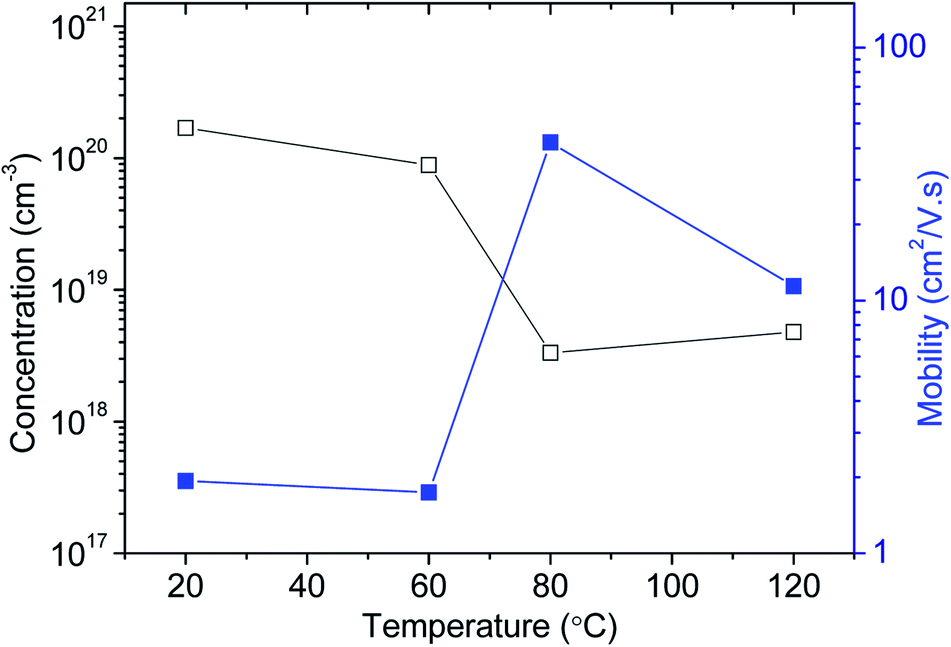 | ||
| Fig. 10 Concentration and mobility of CuI vs. temperature. | ||
4. Conclusion
Thermoelectric p–n modules of CuI-GZO thin films (ca. 300 nm) were fabricated on a flexible and transparent polyimide Kapton® CS substrate. These were successfully electrically interconnected in series and thermally in parallel to produce a maximum power output of 10.83 nW at a temperature difference of 20 °C at an Iout of 0.67 μA.Additionally, a thin film of copper iodide prepared by solid iodination of a copper thin film demonstrated to behave uniquely to different types of forces applied during bending of the flexible substrate. Under compressive forces, a total of 100 cycles at fixed bending radius results in a relatively stable resistance, whereas under tension forces the CuI thin film suffers a maximum change of resistance Rint of 9.1% after 100 bending cycles. Furthermore, the resistance recovery of a sample subjected to tension is possible when a compressive force is subsequently applied.
Moreover, CuI thin films were observed to be electrically unstable at temperatures beyond 80 °C as this stoichiometrically homogenises the film and eliminates vacancy-related electron conductance. Nevertheless, the process is mostly reversible over time, and Rint recovery is achievable with the adsorption of hydroxide molecules at the surface of the thin film – a process commonly observed in oxide semiconductors.
The results presented in here are key to define the potential future applications of CuI thin films in transparent technology, not only in the field of thermoelectrics but on a broader scale of applications requiring simultaneously transparent, flexible, electrically conductive p-type materials.
Conflicts of interest
There are no conflicts to declare.Acknowledgements
This work was mainly funded by H2020-ICT-2014-1, RIA, TransFlexTeg-645241, and ERC-CoG-2014, CapTherPV, 647596, and partially funded by FEDER funds through the COMPETE 2020 Program and National Funds through FCT – Portuguese Foundation for Science and Technology under the project UID/CTM/50025/2019.The authors would like to thank David Sousa and Ana Sofia Taborda for writing the software used for controlling the bending machine and measuring the resistance of the AZO films, and also to Doctor R. C. da Silva for developing the post-processing software, required for determining the relevant parameters per cycle: e.g. bending radius of curvature, initial and final electrical resistances as well as the critical bending radius.References
- M. Grundmann, F. Klüpfel, R. Karsthof, P. Schlupp, F.-L. Schein, D. Splith, C. Yang, S. Bitter and H. von Wenckstern, J. Phys. D: Appl. Phys., 2016, 49, 213001 CrossRef.
- H. Kawazoe, M. Yasukawa, H. Hyodo, M. Kurita, H. Yanagi and H. Hosono, Nature, 1997, 389, 939 CrossRef CAS.
- C. Ruttanapun, W. Kosalwat, C. Rudradawong, P. Jindajitawat, P. Buranasiri, D. Naenkieng, N. Boonyopakorn, A. Harnwunggmoung, W. Thowladda, W. Neeyakorn, C. Thanachayanont, A. Charoenphakdee and A. Wichainchai, Energy Procedia, 2014, 56, 65 CrossRef CAS.
- K. Hayashi, K. I. Sato, T. Nozaki and T. Kajitani, Jpn. J. Appl. Phys., 2008, 47, 59 CrossRef CAS.
- B. M. Morais Faustino, D. Gomes, J. Faria, T. Juntunen, G. Gaspar, C. Bianchi, A. Almeida, A. Marques, I. Tittonen and I. Ferreira, Sci. Rep., 2018, 8, 6867 CrossRef.
- M. K. Yadav and B. Sanyal, Mater. Res. Express, 2014, 1, 015708 CrossRef.
- N. Yamada, R. Ino, H. Tomura, Y. Kondo and Y. Ninomiya, Adv. Electron. Mater., 2017, 3, 1700298 CrossRef.
- S. Qing, A. Rezania, L. A. Rosendahl and X. Gou, Mater. Today: Proc., 2018, 5, 10338 CAS.
- C. Yang, D. Souchay, M. Kneiß, M. Bogner, H. M. Wei, M. Lorenz, O. Oeckler, G. Benstetter, Y. Q. Fu and M. Grundmann, Nat. Commun., 2017, 8, 16076 CrossRef CAS.
- S.-I. Park, J.-H. Ahn, X. Feng, S. Wang, Y. Huang and J. A. Rogers, Adv. Funct. Mater., 2008, 18, 2673 CrossRef CAS.
- M. Grundmann, F.-L. Schein, M. Lorenz, T. Böntgen, J. Lenzner and H. von Wenckstern, Phys. Status Solidi, 2013, 210, 1671 CAS.
- J.-S. Park, J. K. Jeong, H.-J. Chung, Y.-G. Mo and H. D. Kim, Appl. Phys. Lett., 2008, 92, 72104 CrossRef.
| This journal is © The Royal Society of Chemistry 2019 |