 Open Access Article
Creative Commons Attribution 3.0 Unported Licence
Structure and conductivity enhanced treble-shelled porous silicon as an anode for high-performance lithium-ion batteries
Yangfan Lin a,
Hanqing Lina,
Jingwei Jianga,
Deren Yang*a,
Ning Du*a,
Xueqin Heb,
Jianguo Renb,
Peng He
 b,
Chunlei Pangb and
Chengmao Xiaob
aState Key Lab of Silicon Materials, School of Materials Science and Engineering, Zhejiang University, Hangzhou 310027, People's Republic of China. E-mail: dna1122@zju.edu.cn; Fax: +86-571-87952322; Tel: +86-571-87953190
bBTR New Energy Materials Inc, Shenzhen 518106, P. R. China
First published on 1st November 2019
Abstract
Silicon is regarded as the next generation anode material for lithium-ion batteries because of its high specific capacity, low intercalation potential and abundant reserves. However, huge volume changes during the lithiation and delithiation processes and low electrical conductivity obstruct the practical applications of silicon anodes. In this study, a treble-shelled porous silicon (TS-P-Si) structure was synthesized via a three-step approach. The TS-P-Si anode delivered a capacity of 858.94 mA h g−1 and a capacity retention of 87.8% (753.99 mA h g−1) after being subjected to 400 cycles at a current density of 400 mA g−1. The good cycling performance was due to the unique structure of the inner silicon oxide layer, middle silver nano-particle layer and outer carbon layer, leading to a good conductivity and a decreased volume change of this silicon-based anode.
1. Introduction
Rapid development in the field of portable devices, electric vehicles and large-scale energy storage systems demands for high-performance lithium-ion batteries (LIBs) with high energy density, long cycle life, low fabrication cost and good security capability.1–3 Among all the promising next-generation anodes for LIBs, silicon (Si) exhibits the most competitive specific capacity of ∼4200 mA h g−1 (Li22Si5) and reliable safety performances (no lithium metal dendrite formation).4,5 However, its large volume expansion and contraction (∼300%) during lithiation and delithiation processes induce the pulverization of the Si structure, and in consequence leads to a poor cycling stability.6 Besides, the large volume change of Si particles increases the instability of the interface between the electrode and electrolyte, leading to the fracture and repetitive formation of a solid-electrolyte interphase (SEI) film.7 Various structures, such as nanoparticles,8,9 nanotubes,10–12 nanofibers,13,14 core–shell structures,15,16 yolk–shell structures,17,18 and porous structures,19–22 have been synthesized in an effort to buffer the volume expansion during the lithiation process. Among the above-mentioned structures, porous Si with a coating layer attracts considerable attention. Its inner porous structure has enough internal space to accommodate the volume expansion and its cover shell can limit the formation of SEI by avoiding the direct contact of Si and electrolytes.23In the last decade, many attempts have been made to synthesize these Si/carbon porous structures to be used as anode materials in LIBs. Zhang et al. report a three-dimensional bicontinuous silicon anode formed by depositing a Si film on a porous nickel metal template via a chemical vapor deposition (CVD) method. This bicontinuous 3D porous Si anode exhibits an especially high reversible capacity of 2660 mA h g−1 after 100 cycles at a current density of 0.3 C.24 A. Magasinski et al. deposited Si nanoparticles on the surface of carbon black dendritic particles, which were subsequently assembled into a porous rigid spherical granule via CVD.25 The so-called C–Si nanocomposite spherical granules delivered a reversible specific capacity of 1590 mA h g−1 with almost no capacity fading after 100 cycles at a current density of 1 C. The porous Si structure synthesized by the CVD process delivered a good electrochemical performance from the standpoint of specific capacity and cycle life; however, the fabricating cost of a porous Si structure by CVD is an insurmountable challenge for commercial applications. Recently, our group demonstrated a large-scale, low-cost and convenient preparation method of Si@C three-dimensional porous structures via simple annealing and acid pickling processes of home-build magnesium silicide (Mg2Si, ∼5$ per kg).26 These Si@C three-dimensional porous structures can accommodate large volume expansion during the lithiation process and deliver a high reversible capacity of ∼1700 mA h g−1 after 70 cycles. The production technology of porous Si from Mg2Si has a good prospect for mass production; however, the as-synthesized porous Si is subject to structural instability during the lithiation and delithiation processes. In addition, the low conductivity of porous Si is an obstruction for the application of porous Si synthesized from Mg2Si.
Herein, treble shells constituted by an inner silicon oxide layer, a silver (Ag) nanoparticle interlayer and an outermost carbon layer are compounded on the surface of porous silicon. TS-P-Si electrodes exhibit remarkable cycling stability, which can be attributed to the synergistic effect of treble shells, which limit the expansion of silicon during cycling,27,28 improve the electrical conductivity of electrodes29 and eliminate the active materials from electrolytes to prevent unwanted reactions.30
2. Experimental section
2.1. Materials
Mg2Si (purity, >97%) was synthesized through a home-built continuous preparation apparatus using Si (purity, >98%) and Mg (purity, >99%) as the sources. (3-Mercaptopropyl)triethoxysilane (MPTS, GC, >96%, Aladdin, China), HCl (AR, 36%–38%, Sinopharm Chemical Reagent Co., Ltd., China), H2SO4 (AR, 98%, Sinopharm Chemical Reagent Co., Ltd., China), H2O2 (AR, 30%, Sinopharm Chemical Reagent Co., Ltd., China), ammonium hydroxide (AR, 25–28%, Sinopharm Chemical Reagent Co., Ltd., China), polyvinylpyrrolidone (40![[thin space (1/6-em)]](https://www.rsc.org/images/entities/char_2009.gif) 000 wt, Sigma-Aldrich, America), ethylene glycol (GC, >99.5%, Aladdin, China), n-octylamine (GC, >99.5%, Aladdin, China), AgNO3 (>99%, Sigma-Aldrich, America), super P carbon black (CP, Sinopharm Chemical Reagent Co., Ltd., China), sodium carboxymethyl cellulose (∼90
000 wt, Sigma-Aldrich, America), ethylene glycol (GC, >99.5%, Aladdin, China), n-octylamine (GC, >99.5%, Aladdin, China), AgNO3 (>99%, Sigma-Aldrich, America), super P carbon black (CP, Sinopharm Chemical Reagent Co., Ltd., China), sodium carboxymethyl cellulose (∼90![[thin space (1/6-em)]](https://www.rsc.org/images/entities/char_2009.gif) 000, Sigma-Aldrich, America), and electrolyte solutions (Dongguan shanshan battery materials Co., Ltd, China) were used.
000, Sigma-Aldrich, America), and electrolyte solutions (Dongguan shanshan battery materials Co., Ltd, China) were used.
2.2. Synthesis of TS-P-Si
TS-P-Si was synthesized via a three-step approach. First, 5 g Mg2Si powder was thermally treated in air atmosphere at a temperature of 80 °C for 1 h and then the powder was washed using diluted hydrochloric acid (0.2 mol L−1) to remove MgO and any residual Mg2Si. Porous silicon was collected as a precursor after vacuum drying at the temperature of 80 °C. Second, 500 mg of the precursor porous silicon particles were oxidized with a 40 mL solution H2SO4![[thin space (1/6-em)]](https://www.rsc.org/images/entities/char_2009.gif) :
:![[thin space (1/6-em)]](https://www.rsc.org/images/entities/char_2009.gif) H2O2 = 1
H2O2 = 1![[thin space (1/6-em)]](https://www.rsc.org/images/entities/char_2009.gif) :
:![[thin space (1/6-em)]](https://www.rsc.org/images/entities/char_2009.gif) 1 in volume for 10 min to form a silicon oxide (SiOx) layer on the surface and plenty of hydroxyls were introduced on the surface of the silicon layer. Third, 100 μL MPTS and 60 μL aqueous ammonium hydroxide (25–28%) were mixed in 20 mL ethanol, then 200 mg oxidized porous silicon (O-P-Si) particles were dispersed in the above solution and stirred for 12 h at room temperature. The resulting MPTS-connected O-P-Si particles were centrifuged and washed with ethanol for several times and dried at 80 °C. The MPTS-connected O-P-Si particles (60 mg) were dispersed in 75 mL ethylene glycol with 5 mg PVP, then 25 mL AgNO3 solution was added to the MPTS-connected O-P-Si particles solution to obtain a final AgNO3 concentration of 3.5 mmol L−1, and thoroughly mixed. Octylamine (100 μL) was rapidly added in the MPTS-connected O-P-Si and AgNO3 mixed solution, and then the solution was stirred for 1 h. The Ag-coated porous silicon (P-Si/Ag) particles were collected after centrifugation, washed and dried. Finally, the P-Si/Ag particles were coated with a carbon layer via thermal decomposition of acetylene gas at a temperature of 800 °C for 1 h.
1 in volume for 10 min to form a silicon oxide (SiOx) layer on the surface and plenty of hydroxyls were introduced on the surface of the silicon layer. Third, 100 μL MPTS and 60 μL aqueous ammonium hydroxide (25–28%) were mixed in 20 mL ethanol, then 200 mg oxidized porous silicon (O-P-Si) particles were dispersed in the above solution and stirred for 12 h at room temperature. The resulting MPTS-connected O-P-Si particles were centrifuged and washed with ethanol for several times and dried at 80 °C. The MPTS-connected O-P-Si particles (60 mg) were dispersed in 75 mL ethylene glycol with 5 mg PVP, then 25 mL AgNO3 solution was added to the MPTS-connected O-P-Si particles solution to obtain a final AgNO3 concentration of 3.5 mmol L−1, and thoroughly mixed. Octylamine (100 μL) was rapidly added in the MPTS-connected O-P-Si and AgNO3 mixed solution, and then the solution was stirred for 1 h. The Ag-coated porous silicon (P-Si/Ag) particles were collected after centrifugation, washed and dried. Finally, the P-Si/Ag particles were coated with a carbon layer via thermal decomposition of acetylene gas at a temperature of 800 °C for 1 h.
2.3. Characterization
The morphology of the as-prepared samples was characterized via field emission scanning electron microscopy (FESEM, HITACH S4800) and transmission electron microscopy (TEM, PHILIPS F200). Energy dispersive spectroscopy (EDS) mapping images and line scanning images were recorded by a FEI Titan ChemiS TEM equipped with a probe-corrector and a Super-X EDS detector system. X-ray photoelectron spectroscopy (XPS) was performed by employing a Thermo ESCALAB 250Xi spectrometer with a monochromatic Al Kα line (1486.6 eV). The crystal structures of the materials were determined using a high power X-ray diffractometer (XRD) on a Rigaku D/max-ga X-ray diffractometer, where the Cu Kα radiation was 1.54 Å.2.4. Electrochemical characterization
The 2025-type cell, composed of TS-P-Si as the working electrode and lithium metal as the counter electrode, was encapsulated in a glove box (Mbraun, labstar, Germany) under argon atmosphere. The slurry casting on the Cu collector was constituted of active materials (TS-P-Si, P-Si/Ag and O-P-Si), sodium carboxymethyl cellulose (CMC) and super P carbon black, in a mass ratio of 7![[thin space (1/6-em)]](https://www.rsc.org/images/entities/char_2009.gif) :
:![[thin space (1/6-em)]](https://www.rsc.org/images/entities/char_2009.gif) 2
2![[thin space (1/6-em)]](https://www.rsc.org/images/entities/char_2009.gif) :
:![[thin space (1/6-em)]](https://www.rsc.org/images/entities/char_2009.gif) 1. The loading of active materials on the electrode was 2.4 mg cm−2. The electrolyte solution consisted of LiPF6 in dimethyl carbonate (DMC) and ethylene carbonate (EC) (1
1. The loading of active materials on the electrode was 2.4 mg cm−2. The electrolyte solution consisted of LiPF6 in dimethyl carbonate (DMC) and ethylene carbonate (EC) (1![[thin space (1/6-em)]](https://www.rsc.org/images/entities/char_2009.gif) :
:![[thin space (1/6-em)]](https://www.rsc.org/images/entities/char_2009.gif) 1 volume ratio) with 5 vol% fluoroethylene carbonate (FEC) as an additive. The cyclic voltammetry (CV) curve was recorded on a CHI660D system at a scan rate of 0.1 mV s−1. The Nyquist plot was acquired on the CHI660D system in the frequency range from 100 kHz to 100 mHz. The galvanostatic discharge–charge data was collected using a Neware CT-4008-5V50 mA system in the potential range of 0.001–1.2 V.
1 volume ratio) with 5 vol% fluoroethylene carbonate (FEC) as an additive. The cyclic voltammetry (CV) curve was recorded on a CHI660D system at a scan rate of 0.1 mV s−1. The Nyquist plot was acquired on the CHI660D system in the frequency range from 100 kHz to 100 mHz. The galvanostatic discharge–charge data was collected using a Neware CT-4008-5V50 mA system in the potential range of 0.001–1.2 V.
3. Results and discussion
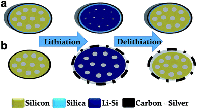
Scheme 1 shows a representation of the structural transformations of TS-P-Si (a) and bare carbon-shelled porous Si (b) during the lithiation/delithiation process. As shown in Scheme 1a, the robust treble-shelled system constituted of a silicon oxide layer, a Ag nanoparticle layer and a carbon layer, in which the silicon oxide layer has a strong constraining effect and limits the outward expansion tendency of the inner Si. Consequently, Si tends to expand inward to fill its internal porosity during the lithiation process. Due to abundant voids in the porous Si that can accommodate the expansion of Si, the whole TS-P-Si structure will remain stable and even afford no volume change during the lithiation and delithiation processes. Therefore, the silica layer can maintain structural integrity and the outmost carbon layer can ensure the isolation of the internal active material from electrolytes to prevent side reactions after long cycles.31 However, for the carbon-shelled porous silicon, as shown in Scheme 1b, the carbon layer will be destroyed without a structural support, and the freshly exposed surface of active materials will produce side reactions with the electrolyte solution and eventually lead to the repeated regeneration of the SEI film and cause electrical isolation between the active materials.TS-P-Si is synthesized via a three-step approach: first, porous Si was oxidized with a mixture of concentrated sulfuric acid and hydrogen peroxide in a ratio of 1![[thin space (1/6-em)]](https://www.rsc.org/images/entities/char_2009.gif) :
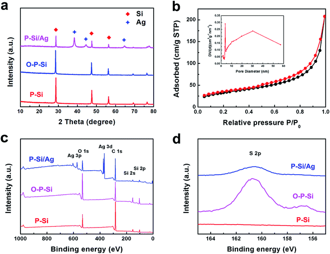
:![[thin space (1/6-em)]](https://www.rsc.org/images/entities/char_2009.gif) 1 in volume for 10 min, to form a silicon oxide layer on the surface; second, Ag nanoparticles are deposited on the surface of the silicon oxide layer through a Ag mirror reaction;32 third, the outmost carbon layer is obtained via acetylene thermal decomposition. Fig. 1a shows the XRD patterns of the products along the synthetic process. As can be seen, P-Si/Ag exhibits the typical {1 1 1}, {2 2 0}, {3 1 1} planes of crystalline Si (JCPDS no. 27-1402) and {1 1 1}, {2 0 0}, {2 2 0} planes of crystalline Ag (JCPDS no. 04-0783). In addition, no distinctive amorphous phase distinguished from the XRD patterns of O-P-Si and P-Si/Ag indicates that the thickness of the silicon oxide layer is low. Therefore, the silicon oxide layer will just consume a limited amount of lithium and has no significant influence on the first coulombic efficiency of the TS-P-Si anodes. The average size of Ag particles calculated via the Scherrer equation is 16.9 nm. BET analysis was conducted to estimate the porosity of TS-P-Si after the carbon coating process. As shown in Fig. 1b, TS-P-Si has a BET surface area of 117.05 m2 g−1 with an average Barrett–Joyner–Halenda (BJH) pore diameter of 12.4 nm, indicating that the porous structure still remained unchanged after the deposition of the carbon shell. Furthermore, XPS was employed to analyze the surface state transformation during the synthetic process of the Ag nanoparticle layer. In order to deposit the Ag nanoparticles on the surface of porous Si, a hydroxysulphonyl group was introduced on the surface of porous Si first via the coupling effect of hydroxyl groups on the surface of the silicon oxide layer and (3-mercaptopropyl) triethoxysilane. After hydroxysulphonyls collect Ag ions on the surface of porous Si, an Ag nanoparticle layer could be synthesized after the reduction of the Ag ions by n-octylamine.33 Fig. 1c shows the XPS spectra of O-P-Si, MPTS-connected O-P-Si and P-Si/Ag, indicating that the Ag nanoparticles have been deposited on the surface. Fig. 1d shows the S 2p XPS spectra of P-Si, MPTS-connected O-P-Si and P-Si–Ag. As can be seen, the sulfur element appears on the surface of O-P-Si particles after MPTS treatment and decreases after Ag nanoparticle deposition, which can demonstrate that the sulfhydryl moiety is connected on the surface of O-P-Si nanoparticles and consumed during the Ag nanoparticle deposition process.
1 in volume for 10 min, to form a silicon oxide layer on the surface; second, Ag nanoparticles are deposited on the surface of the silicon oxide layer through a Ag mirror reaction;32 third, the outmost carbon layer is obtained via acetylene thermal decomposition. Fig. 1a shows the XRD patterns of the products along the synthetic process. As can be seen, P-Si/Ag exhibits the typical {1 1 1}, {2 2 0}, {3 1 1} planes of crystalline Si (JCPDS no. 27-1402) and {1 1 1}, {2 0 0}, {2 2 0} planes of crystalline Ag (JCPDS no. 04-0783). In addition, no distinctive amorphous phase distinguished from the XRD patterns of O-P-Si and P-Si/Ag indicates that the thickness of the silicon oxide layer is low. Therefore, the silicon oxide layer will just consume a limited amount of lithium and has no significant influence on the first coulombic efficiency of the TS-P-Si anodes. The average size of Ag particles calculated via the Scherrer equation is 16.9 nm. BET analysis was conducted to estimate the porosity of TS-P-Si after the carbon coating process. As shown in Fig. 1b, TS-P-Si has a BET surface area of 117.05 m2 g−1 with an average Barrett–Joyner–Halenda (BJH) pore diameter of 12.4 nm, indicating that the porous structure still remained unchanged after the deposition of the carbon shell. Furthermore, XPS was employed to analyze the surface state transformation during the synthetic process of the Ag nanoparticle layer. In order to deposit the Ag nanoparticles on the surface of porous Si, a hydroxysulphonyl group was introduced on the surface of porous Si first via the coupling effect of hydroxyl groups on the surface of the silicon oxide layer and (3-mercaptopropyl) triethoxysilane. After hydroxysulphonyls collect Ag ions on the surface of porous Si, an Ag nanoparticle layer could be synthesized after the reduction of the Ag ions by n-octylamine.33 Fig. 1c shows the XPS spectra of O-P-Si, MPTS-connected O-P-Si and P-Si/Ag, indicating that the Ag nanoparticles have been deposited on the surface. Fig. 1d shows the S 2p XPS spectra of P-Si, MPTS-connected O-P-Si and P-Si–Ag. As can be seen, the sulfur element appears on the surface of O-P-Si particles after MPTS treatment and decreases after Ag nanoparticle deposition, which can demonstrate that the sulfhydryl moiety is connected on the surface of O-P-Si nanoparticles and consumed during the Ag nanoparticle deposition process.
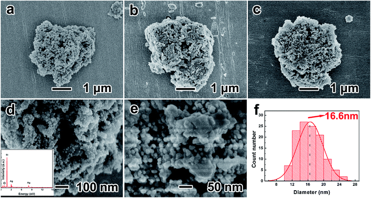
Fig. 2a–c show the low-resolution SEM images of porous silicon, O-P-Si and P-Si/Ag, suggesting that the porous structure has a diameter of ∼3 μm. Porous silicon is constituted primarily by Si nanoparticles, and the space between particles composes the porous structure. After the oxidation process, the silicon oxide layer connects the adjacent nanoparticles on their surfaces and the resulting O-P-Si has higher structural integrity. Fig. 2c shows the morphology of the uniform deposition of a Ag layer on the surface of porous silicon. The high-resolution SEM image of P-Si/Ag demonstrates that the Ag nanoparticles are compactly attached on the surface of porous silicon (Fig. 2d). The EDS spectra in the inset of Fig. 2d show that the elemental composition of Si, Ag and O are 59.36%, 21.34% and 19.31%, respectively. Fig. 2f shows the diameter statistical distribution diagram for Ag nanoparticles on the surface of the P-Si/Ag from Fig. 2e. It can be seen that the average diameter of Ag nanoparticles is ∼16.6 nm, which corresponds to the calculated result via the Scherrer equation.
The EDS elemental mapping of Ag nanoparticle-coated porous Si (Fig. 3a and b) was conducted to estimate the distribution of major elements (Si, Ag and O). It can be noticed that Si is distributed in the whole porous structure and elements such as Ag and O are distributed only on the surface of porous Si. Fig. 3c shows the HRTEM image of the sandwich construction contributed by inner Si, the middle silicon oxide layer and outer Ag nanoparticles. The lattice distances of ∼0.31 and ∼0.12 nm correspond to the {1 1 1} face of Si and the {2 0 2} face of Ag, respectively. Between the inner Si and Ag nanoparticle layer, the silicon oxide layer has a thickness of ∼5 nm. It should be mentioned that an appropriate thickness of the silicon oxide layer is vital for the electrochemical performance of the Si anode.34 The silicon oxide layer can maintain the structure stability of porous Si during multiple cycles; however, a thick silicon oxide layer will consume too much of the lithium source, resulting in the lowering of the initial coulombic efficiency and a poor electrical conductivity. In addition, the EDS elemental line scanning of Ag nanoparticle-coated porous Si (Fig. 3d) demonstrates that the elements of Ag and O are uniformly distributed on the surface of Si.
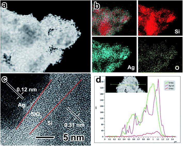 | ||
| Fig. 3 (a and b) EDX elemental mapping of P-Si/Ag; (c) high-magnification TEM image of P-Si–Ag; (d) EDX elemental line scanning of P-Si/Ag. | ||
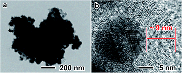
TS-P-Si was synthesized after carbon coating through acetylene thermal decomposition. Fig. 4 shows the TEM images of TS-P-Si. It can be seen that a uniform carbon layer covers the whole porous structure, as shown in Fig. 4a. The high-magnification TEM image in Fig. 4b shows that the thickness of the carbon layer is ∼9 nm.
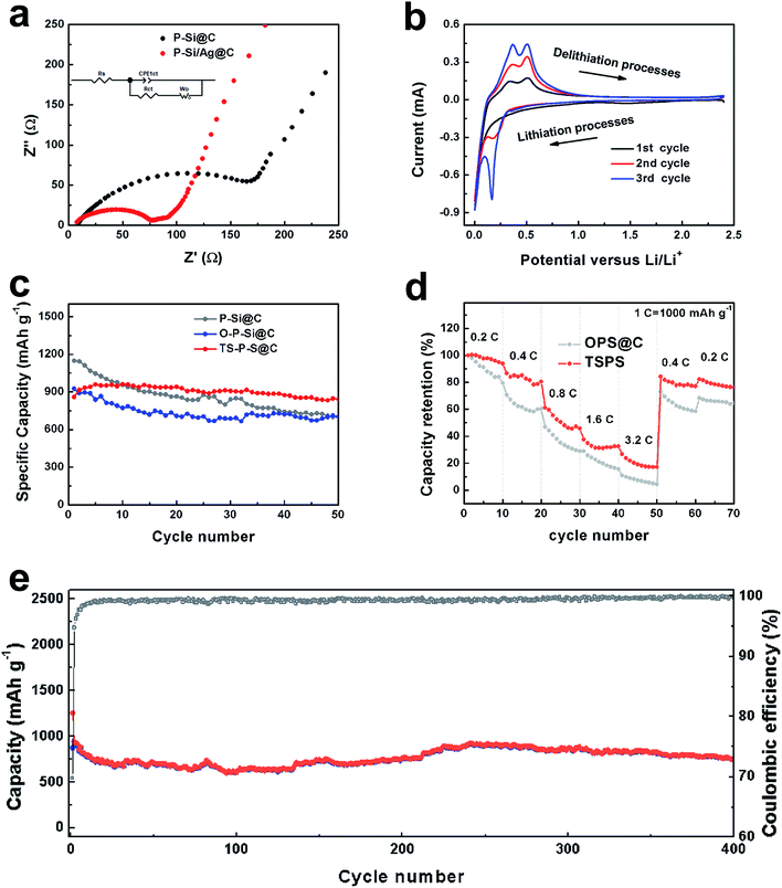
To further corroborate the stability of the TS-P-Si structure during lithiation and delithiation processes, the TS-P-Si particles were used to prepare an anode, and then evaluated their electrochemical performance in LIBs. Fig. 5a shows the Nyquist plots of bare carbon-coated porous silicon (P-Si@C) and TS-P-Si (before a cycle) obtained by applying a sinusoidal current over the frequency range of 100 kHz–0.01 Hz. The illustration insertion shows the equivalent circuit of the EIS impedance simulation. Rs represents the internal impedance of the tested LIBs, while Rct and CPEct correspond to the charge-transfer resistance and the constant phase element of the interface between electrode and electrolyte, respectively. Wo is associated with the Warburg impedance, corresponding to the Li-ion diffusion process.35 As shown in Fig. 5a, the semicircle on the medium-frequency region corresponds to the Rct and CPEct of the electrode/electrolyte interface, and the sloping line in the low-frequency region corresponds to the lithium-ion diffusion process within the electrode materials. The charge-transfer differences of P-Si@C and TS-P-Si were investigated by further modeling AC impedance spectra based on a modified equivalent circuit. The fitted Rct quantitative values for P-Si@C and TS-P-Si are 176.4 and 72.9 Ω, respectively, indicating that the Ag nanoparticle layer can act as a current collector network to improve the electrical conductivity and accelerate the electron transport during the lithiation/delithiation processes, resulting in a significant improvement in the electrochemical performance of the TS-P-Si anode.
Fig. 5b shows the typical cyclic voltammetry (CV) curve of an anode prepared by TS-P-Si, tested in the range 0.01–2.5 V versus Li/Li+ at a scanning rate of 0.1 mV s−1. In the first cycle, two cathodic peaks located at 0.01 V, and two anodic peaks located at 0.38 and 0.51 V can be observed, corresponding to the reversible lithiation/delithiation process of Si.36 In the subsequent two cycles, the current intensity of the redox peaks increases gradually and the location of redox peaks remains at the same potential value, indicating an increased speed of the lithiation/delithiation reaction.37 Fig. 5c shows a comparison of the electrochemical performances of P-Si@C, carbon-coated oxidized porous silicon (O-P-Si@C) and treble-shelled porous silicon (TS-P-Si). Table 1 counts the electrochemical performances of the above materials after 50 cycles. O-P-Si@C electrodes, with a 75.80% capacity retention, show a much better cycling performance than P-Si@C (with only 61.48% capacity retention). This can be attributed to the stable structure of the silicon oxide layer, which can buffer the volume expansion of the inner silicon structure during cycles. As a result, the O-P-Si@C structures can maintain the stability of the SEI and deliver stable cycling performance. Furthermore, the best electrochemical performance of the TS-P-Si electrodes can be attributed to the excellent electrical conductivity of Ag, which can be seen in the EIS test in Fig. 5a. Fig. 5d shows the rate performance of the O-P-Si@C and TS-P-Si electrodes. The O-P-Si@C shows 84.02%, 60.35%, 28.84%, 15.63%, 4.48%, 58.94%, 64.53% capacity retentions at the current densities of 0.2C, 0.4C, 0.8C, 1.6C, 3.2C and then back to 0.4C and 0.2C, respectively. For comparison, TS-P-Si shows 93.84%, 80.52%, 45.82%, 32.55%, 17.13%, 77.17%, 76.34% capacity retentions under the similar conditions. Eventually, TS-P-Si was subjected to tests on cycling stability over multiple cycles. As shown in Fig. 5e, TS-P-Si preserves about 753.99 mA h g−1 charge capacity (∼87.8% capacity retention to first charge) after 400 cycles, showing particularly good cycling stability.
| 1st Capacity (mA h g−1) | 50th Capacity (mA h g−1) | Capacity retention (%) | |
|---|---|---|---|
| P-Si@C | 1148.06 | 705.80 | 61.48 |
| O-P-Si@C | 925.28 | 701.40 | 75.80 |
| TS-P-Si | 858.94 | 841.64 | 97.99 |
During the lithiation and delithiation processes, the silicon oxide layer and the carbon layer can maintain the structure stability of TS-P-Si. In addition, the Ag nanoparticle layer and carbon layer can maintain the electrical conductivity of the treble-shelled porous structure. The synergistic effects of treble shells contribute to the especially stable electrochemical performance of the TS-P-Si anode. Fig. 6 shows the TEM images of TS-P-Si after 50th cycle at a current density of 400 mA h g−1. As can be seen, the integrity of treble-shelled porous structures is maintained after 50th cycle (Fig. 6a), and the Ag nanoparticles remain in their initial phase without reacting with lithium ions, as the lattice distance of ∼0.20 nm is definitely identified as the {103} face of Ag (Fig. 6b); and always act as a current collector on the surface of TS-P-Si during the charge/discharge process. TS-P-Si has a stable structure that will not be destructed by the stress induced by the volume expansion/shrinkage of inner silicon during the cycling process. Simultaneously, TS-P-Si can maintain the intact conductive network consisting of Ag nanoparticles and a carbon layer in the protection of silicon oxide layer. As a consequence, the TS-P-Si delivers an excellent electrochemical performance as anode materials for LIBs.
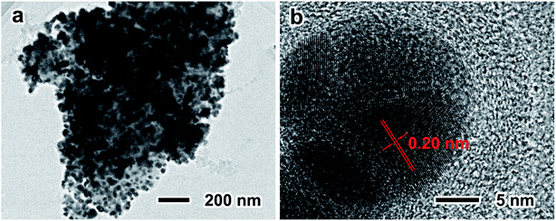 | ||
| Fig. 6 Low- (a) and high-magnification TEM (b) images of TS-P-Si after 50 cycle times at a current density of 400 mA h g−1. | ||
4. Conclusion
In summary, a novel treble-shelled porous silicon structure with structural-enhanced and electrical conductivity-enhanced layers was synthesized via a three-step approach. Due to the protection ability of an inner silicon oxide layer and an outer carbon layer, TS-P-Si can maintain structural stability during lithiation and delithiation processes. Furthermore, the middle Ag nanoparticle layer and outer carbon layer can improve the electrical conductivity of the integral structure of porous silicon. Therefore, the treble-shelled porous silicon anode delivered an ultra-stable cycling life (86.14% capacity retention after 400 cycles at a current density of 400 mA g−1) as an anode material for LIBs.Conflicts of interest
There are no conflicts to declare.Acknowledgements
The authors would like to appreciate the financial supports from the Fundamental Research Funds for the Central Universities and the Foundation for Innovative Research Groups of the National Natural Science Foundation of China (Grant No. 61721005).References
- J. M. Tarascon and M. Armand, Issues and challenges facing rechargeable lithium batteries, Nature, 2001, 414, 359–367 CrossRef CAS PubMed.
- M. Armand and J. M. Tarascon, Building better batteries, Nature, 2008, 451, 652–657 CrossRef CAS.
- B. Scrosati, J. Hassoun and Y.-K. Sun, Lithium-ion batteries. A look into the future, Energy Environ. Sci., 2001, 4, 3287–3295 RSC.
- H. Wu, G. Chan, J. W. Choi, I. Ryu, Y. Yao, M. T. McDowell, S. W. Lee, A. Jackson, Y. Yang, L. Hu and Y. Cui, Stable cycling of double-walled silicon nanotube battery anodes through solid–electrolyte interphase control, Nat. Nanotechnol., 2012, 7, 310–315 CrossRef CAS.
- X. H. Liu and J. Y. Huang, In situ TEM electrochemistry of anode materials in lithium ion batteries, Energy Environ. Sci., 2011, 4, 3844 RSC.
- M. A. Rahman, G. Song, A. I. Bhatt, Y. C. Wong and C. Wen, Nanostructured Silicon Anodes for High-Performance Lithium-Ion Batteries, Adv. Funct. Mater., 2016, 26, 647–678 CrossRef CAS.
- H. Wu and Y. Cui, Designing nanostructured Si anodes for high energy lithium ion batteries, Nano Today, 2012, 7, 414–429 CrossRef CAS.
- X. H. Liu, L. Zhong, S. Huang, S. X. Mao, T. Zhu and J. Y. Huang, Size-Dependent Fracture of Silicon Nanoparticles During Lithiation, ACS Nano, 2012, 6, 1522–1531 CrossRef CAS.
- G. Lv, B. Zhu, X. Li, C. Chen, J. Li, Y. Jin, X. Hu and J. Zhu, Simultaneous Perforation and Doping of Si Nanoparticles for Lithium-Ion Battery Anode, ACS Appl. Mater. Interfaces, 2017, 9, 44452–44457 CrossRef CAS.
- H. Wu, G. Chan, J. W. Choi, I. Ryu, Y. Yao, M. T. McDowell, S. W. Lee, A. Jackson, Y. Yang, L. Hu and Y. Cui, Stable cycling of double-walled silicon nanotube battery anodes through solid–electrolyte interphase control, Nat. Nanotechnol., 2012, 7, 310–315 CrossRef CAS.
- A. T. Tesfaye, R. Gonzalez, J. L. Coffer and T. Djenizian, Porous Silicon Nanotube Arrays as Anode Material for Li-Ion Batteries, ACS Appl. Mater. Interfaces, 2015, 7, 20495–20498 CrossRef CAS.
- Q. Xiao, Y. Fan, X. Wang, R. A. Susantyoko and Q. Zhang, A multilayer Si/CNT coaxial nanofiber LIB anode with a high areal capacity, Energy Environ. Sci., 2014, 7, 655–661 RSC.
- Y. Chen, N. Du, H. Zhang and D. Yang, Porous Si@C coaxial nanotubes: layer-by-layer assembly on ZnO nanorod templates and application to lithium-ion batteries, CrystEngComm, 2017, 19, 1220–1229 RSC.
- D. J. Lee, H. Lee, M. Ryou, G. Han, J. Lee, J. Song, J. Choi, K. Y. Cho, Y. M. Lee and J. Park, Electrospun Three-Dimensional Mesoporous Silicon Nanofibers as an Anode Material for High-Performance Lithium Secondary Batteries, ACS Appl. Mater. Interfaces, 2013, 5, 12005–12010 CrossRef CAS.
- H. Liu, Z. Shan, W. Huang, D. Wang, Z. Lin, Z. Cao, P. Chen, S. Meng and L. Chen, Self-Assembly of Silicon@Oxidized Mesocarbon Microbeads Encapsulated in Carbon as Anode Material for Lithium-Ion Batteries, ACS Appl. Mater. Interfaces, 2018, 10, 4715–4725 CrossRef CAS.
- Y. Xing, T. Shen, T. Guo, X. Wang, X. Xia, C. Gu and J. Tu, A novel durable double-conductive core-shell structure applying to the synthesis of silicon anode for lithium ion batteries, J. Power Sources, 2018, 384, 207–213 CrossRef CAS.
- N. Liu, H. Wu, M. T. McDowell, Y. Yao, C. Wang and Y. Cui, A Yolk-Shell Design for Stabilized and Scalable Li-Ion Battery Alloy Anodes, Nano Lett., 2012, 12, 3315–3321 CrossRef CAS.
- J. Jiang, H. Zhang, J. Zhu, L. Li, Y. Liu, T. Meng, L. Ma, M. Xu, J. Liu and C. M. Li, Putting Nanoarmors on Yolk–Shell Si@C Nanoparticles: A Reliable Engineering Way to Build Better Si-Based Anodes for Li-Ion Batteries, ACS Appl. Mater. Interfaces, 2018, 10, 24157–24163 CrossRef CAS.
- H. Kim, B. Han, J. Choo and J. Cho, Three-Dimensional Porous Silicon Particles for Use in High-Performance Lithium Secondary Batteries, Angew. Chem., Int. Ed., 2008, 47, 10151–10154 CrossRef CAS.
- P. Guan, J. Li, T. Lu, T. Guan, Z. Ma, Z. Peng, X. Zhu and L. Zhang, Facile and Scalable Approach to Fabricate Granadilla-like Porous-Structured Silicon-Based Anode for Lithium Ion Batteries, ACS Appl. Mater. Interfaces, 2018, 10, 34283–34290 CrossRef CAS.
- Y. Zhang, N. Du, Y. Chen, Y. Lin, J. Jiang, H. He, Y. Lei and D. Yang, Carbon dioxide as a green carbon source for the synthesis of carbon cages encapsulating porous silicon as high performance lithium-ion battery anodes, Nanoscale, 2018, 10, 5626–5633 RSC.
- Y. Chen, Y. Lin, N. Du, Y. Zhang, H. Zhang and D. Yang, A critical SiOx layer on Si porous structures to construct highly-reversible anode materials for lithium-ion batteries, Chem. Commun., 2017, 53, 6101–6104 RSC.
- H. Wu, N. Du, X. Shi and D. Yang, Rational design of three-dimensional macroporous silicon as high performance Li-ion battery anodes with long cycle life, J. Power Sources, 2016, 331, 76–81 CrossRef CAS.
- H. Zhang and P. V. Braun, Three-Dimensional Metal Scaffold Supported Bicontinuous Silicon Battery Anodes, Nano Lett., 2012, 12, 2778–2783 CrossRef CAS.
- A. Magasinski, P. Dixon, B. Hertzberg, A. Kvit, J. Ayala and G. Yushin, High-performance lithium-ion anodes using a hierarchical bottom-up approach, Nat. Mater., 2010, 9, 353–358 CrossRef CAS.
- C. Xiao, N. Du, X. Shi, H. Zhang and D. Yang, Large-scale synthesis of Si@C three-dimensional porous structures as high-performance anode materials for lithium-ion batteries, J. Mater. Chem. A, 2014, 2, 20494–20499 RSC.
- X. Fan, J. Zhao, Z. Yang and W. Zhang, A fluoride ion-mediated continuous etching–redeposition strategy to synthesize Si nanocomposites with appropriate SiO2 coating layers for Li-ion batteries, Chem. Commun., 2018, 54, 12447–12450 RSC.
- Y. Liu, L. Qin, F. Liu, Y. Fan, J. Ruan and S. Zhang, Interpenetrated 3D porous silicon as high stable anode material for Li-Ion battery, J. Power Sources, 2018, 406, 167–175 CrossRef CAS.
- Y. Yu, L. Gu, C. Zhu, S. Tsukimoto, P. A. van Aken and J. Maier, Reversible Storage of Lithium in Silver-Coated Three-Dimensional Macroporous Silicon, Adv. Mater., 2010, 22, 2247–2250 CrossRef CAS PubMed.
- B. Li, S. Li, Y. Jin, J. Zai, M. Chen, A. Nazakat, P. Zhan, Y. Huang and X. Qian, Porous Si@C ball-in-ball hollow spheres for lithium-ion capacitors with improved energy and power densities, J. Mater. Chem. A, 2018, 6, 21098–21103 RSC.
- J. Xie, H. Zhang, J. Chu, W. Shen, R. Chen and J. Yu, Critical SiO2 nanolayers for improving corrosion resistance and lithium storage performances of core-shell nano-Si/C composites, J. Alloys Compd., 2018, 769, 1072–1079 CrossRef CAS.
- C. Luo, Y. Zhang, X. Zeng, Y. Zeng and Y. Wang, The role of poly(ethylene glycol) in the formation of silver nanoparticles, J. Colloid Interface Sci., 2005, 288, 444–448 CrossRef CAS.
- J. Yang, H. Kang, H. Lee, A. Jo, S. Jeong, S. Jeon, H. Kim, H. Lee, D. H. Jeong, J. Kim and Y. Lee, Single-Step and Rapid Growth of Silver Nanoshells as SERS-Active Nanostructures for Label-Free Detection of Pesticides, ACS Appl. Mater. Interfaces, 2014, 6, 12541–12549 CrossRef CAS.
- D. Shen, C. Huang, L. Gan, J. Liu, Z. Gong and M. Long, Rational Design of Si@SiO2/C Composites Using Sustainable Cellulose as a Carbon Resource for Anodes in Lithium-Ion Batteries, ACS Appl. Mater. Interfaces, 2018, 10, 7946–7954 CrossRef CAS.
- S. S. Zhang, K. Xu and T. R. Jow, EIS study on the formation of solid electrolyte interface in Li-ion battery, Electrochim. Acta, 2006, 51, 1636–1640 CrossRef CAS.
- Y. Cen, Y. Fan, Q. Qin, R. D. Sisson, D. Apelian and J. Liang, Synthesis of Si anode with a microsized-branched structure from recovered Al scrap for use in Li-Ion batteries, J. Power Sources, 2019, 410–411, 31–37 CrossRef CAS.
- J. Shi, Y. Liang, L. Li, Y. Peng and H. Yang, Evaluation of the electrochemical characteristics of silicon/lithium titanate composite as anode material for lithium ion batteries, Electrochim. Acta, 2015, 155, 125–131 CrossRef CAS.
| This journal is © The Royal Society of Chemistry 2019 |

