
 Open Access Article
 This Open Access Article is licensed under a Creative Commons Attribution-Non Commercial 3.0 Unported Licence
A light emitter based on practicable and mass-producible polycrystalline graphene patterned directly on silicon substrates from a solid-state carbon source
Kenta Nakagawa ab,
Hidenori Takahashia,
Yui Shimuraa and
Hideyuki Maki*ac
ab,
Hidenori Takahashia,
Yui Shimuraa and
Hideyuki Maki*ac
aDepartment of Applied Physics and Physico-Informatics, Keio University, 3-14-1 Hiyoshi, Kohoku-ku, Yokohama, Kanagawa 223-8522, Japan. E-mail: maki@appi.keio.ac.jp
bKanagawa Institute of Industrial Science and Technology (KISTEC), 705-1 Shimoimaizumi, Ebina, Kanagawa 243-0435, Japan
cCenter for Spintronics Research Network, Keio University, 3-14-1 Hiyoshi, Kohoku-ku, Yokohama, Kanagawa 223-8522, Japan
First published on 21st November 2019
Abstract
We developed a procedure for direct patterning of graphene with arbitrary position, size, and shape on silicon substrates from a solid-state carbon source without dry etching processing. Our light emitting graphene devices perform on a par with those based on high crystallinity graphene obtained via mechanical exfoliation or chemical vapor deposition.
Introduction
Nano-carbon materials such as carbon nanotubes and graphene are promising candidates for next-generation optoelectronic devices such as light emitters1–8 and detectors9 owing to their unique electronic and optical properties.8,10–12 Optical interconnects and silicon photonics are two key technologies for next-generation communication, and nano-carbon materials are regarded as one of the possible candidates for integrated optoelectronic devices because they can be easily integrated on silicon chips.2,4,6,9,13,14Graphene light emitters integrated on silicon chips are being developed as an alternative to conventional light sources based on compound semiconductors.15 The thermal radiation generated by transforming an electrical current into Joule heat in graphene was firstly observed by Freitag et al.16 The emission spectra from graphene are well modelized by the formula for a grey body (Planck's law modified by the emissivity value). This suggests that graphene behaves like a grey body. Luxmoore et al. also investigated the thermal emission from chemical vapor deposition (CVD) grown graphene samples of large area.17 Their studies revealed that the light emission is determined by the distribution of the resistance owing to the spatial distribution of the charge density in the graphene. In addition, Kim et al. found that the thermal radiation efficiency of graphene was 1000 times enhanced by suspending the material.12 Moreover, encapsulating graphene with hexagonal boron nitride layers enhances the thermal radiation efficiency and the visible light emission by changing the local optical density of states.18 Recently, high-speed emitters, which can be modulated with less than 100 ps response time (10 GHz frequency), which is 107 faster than conventional incandescent lamps, have been developed. Miyoshi et al.7 revealed that such a fast modulation is possible thanks to the small heat capacity of graphene and its high heat dissipation towards the substrate due not only to classical thermal transport but also to remote quantum thermal transport via the surface polar phonons of the substrates. They have also demonstrated optical communications based on eye-pattern analysis at 1 Mbps and real-time waveform detection at 50 MHz. All these experimental and theoretical knowledge related to graphene light emitters are important steps forward to open new avenues for integrated optoelectronic devices.
A methodology for mass-production of graphene light emitters on silicon chips is highly sought after and extremely valuable for the industry. In general, graphene sheets are conventionally obtained by (i) mechanical exfoliation method19 or (ii) CVD.20–26 In the mechanical exfoliation method, graphene sheets are mechanically exfoliated from highly ordered pyrolytic graphite and transferred onto the substrates. Graphene obtained by this easy and low-cost method show high crystallinity but transfer position, size and shape, as well as the number of layers cannot be controlled. This is not compatible with practical applications and integration. In the CVD method, graphene sheets are synthesized by chemically reacting a hydrocarbon gas such as a CH4 gas and a metal catalyst substrate such as a Cu single-crystal at high temperature. Graphene sheets obtained by this method are scalable to large dimensions and uniform, but an additional processing step is required to transfer the graphene from the conductive metal catalyst substrates to silicon substrates. Since both methods require a transferring process, graphene growth methods that allow for direct formation on silicon substrates have been sought after and several attempts have been reported.27–40
In this study, we developed a procedure to grow graphene from a solid-state carbon source directly on silicon substrates. To reduce the complexity of the process, the number of steps, and the cost, we have also developed a direct patterning procedure that allows to produce graphene samples with arbitrary position, size, and shape: notably this procedure does not require any dry etching process. Our growth technique is viable for mass production, but the graphene obtained is polycrystalline. This is not a real issue, though, since we have demonstrated that our polycrystalline graphene operates in light emitting devices as well as high crystallinity graphene obtained by mechanical exfoliation method or CVD.
Results and discussions
Growing procedure of graphene directly on silicon substrates from solid-state carbon source
Fig. 1 illustrates schematically the steps of our procedure to grow graphene directly on silicon substrates from a solid-state carbon source. Single side polished Si wafers were used as substrates. SiO2 with a thickness of 300 nm was deposited on the substrates by thermal oxidation. The organic nanoparticles remaining on the surface of the substrates were incinerated by O2 plasma. Then, Ni (20 nm)/amorphous carbon (a-C) (5 nm)/Ni (5 nm) stacked films were deposited by vacuum vapor deposition (Fig. 1(a)). Ni and a-C were used as metal catalyst and solid carbon source, respectively. The a-C was deposited by the thermal evaporation of carbon fiber threads.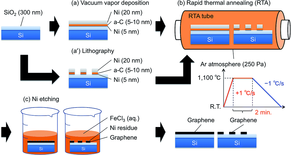 | ||
| Fig. 1 Summary of the growing procedure of graphene directly patterned on silicon substrates from solid-state carbon source. The procedure is divided into three main steps: vacuum vapor deposition (a), rapid thermal annealing (RTA) (b), and Ni etching (c). The resist patterns are designed by conventional lithography technique (a′) before the RTA process; graphene position, size, and shape are controllable. | ||
In this study, rapid thermal annealing (RTA) is utilized to synthesize graphene as an alternative to CVD. This allows for time saving thanks to the much shorter annealing times of RTA processes in comparison to CVD processes. The Ni/a-C/Ni coated substrates were loaded into an RTA furnace. The RTA tube was repeatedly purged with Ar gas for 3 times to substitute the atmosphere of the tube. Then the RTA tube was evacuated and maintained at 250 Pa. The substrates were then heated up from room temperature to 1100 °C at a heating rate of +15 °C s−1, and annealed at 1100 °C steadily for 2 min. A controlled descent back to room temperature was then performed at a cooling rate of 1 °C s−1 (Fig. 1(b)).
After the RTA process, the substrates were immersed in an acid solution FeCl3 (aq.) for about 24 hours to etch the metal catalyst Ni (Fig. 1(c)). Then, the substrates were rinsed several times in deionized water and dried with N2 gas.
Characterization of the graphene
An optical microscope image of the graphene is shown in Fig. 2(a). Large-scale graphene covers the whole area of the substrate and no obvious defects or wrinkles can be observed.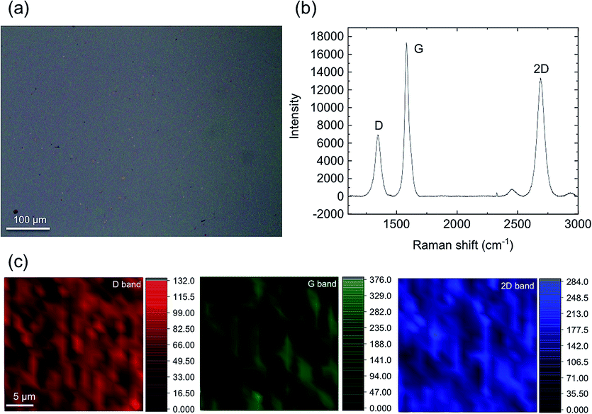 | ||
| Fig. 2 Optical microscope image (a), Raman spectrum (b) and the D, G, and 2D band Raman mapping images (c) of the graphene. | ||
The quality of the graphene was assessed using Raman spectroscopy and mapping. Fig. 2(b) shows the Raman spectrum. The three most pronounced peaks in this spectrum are the D peak at 1346 cm−1, the G peak at 1584 cm−1 and the 2D peak at 2691 cm−1. It is well-known that the intensity ratio of the 2D band to the G band (I2D/IG) becomes smaller as the number of graphene layers is increased.22,41,42 The I2D/IG intensity ratio is about 0.757 indicating that there are just a few layers of graphene. The observation of the D peak, originated by the presence of defects in the crystal lattice,43 indicates that the graphene is polycrystalline. Fig. 2(c) shows the D, G, and 2D band Raman mapping images obtained from a 26 μm × 26 μm region. The intensities of each of the Raman bands in the region are almost the same, indicating that the polycrystalline graphene is almost homogeneous.
Contrary to some previous reports,32,35 the Ni etching process is required to remove all the traces of the metal catalyst Ni. Actually, we have found no evidence supporting the idea that the Ni fully evaporates during the RTA process above 800 °C. This is also confirmed by scanning electron microscope (SEM), energy dispersive X-ray spectroscopy (EDX) and X-ray diffraction (XRD) results. SEM images of the graphene taken before and after the Ni etching process are shown in Fig. 3(a) and (c). Many round-shaped particles can be observed on the surface before the etching process. By elemental analysis with EDX, we found that these round-shaped particles contain a large amount of Ni and Ne impurities. The particles were successfully removed by the Ni etching process as shown in Fig. 3(b) and (d). The XRD results, shown in Fig. 3(e), also support the significance of the Ni etching process as the XRD peak due to Ni (111) at 2θ = 44.6 deg completely disappears after the Ni etching process.
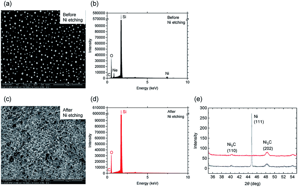 | ||
| Fig. 3 SEM (a and c), EDX (b and d) and XRD (e) results obtained before and after the Ni etching process. EDX analysis revealed that the proportion of the number of C, O, Si, and Ni atoms before (after) Ni etching process is (in percentages) 3.43 (1.93), 28.44 (28.22), 65.98 (69.81), and 1.28 (0.04), respectively. | ||
However, the nickel carbides Ni3C on the substrate, which are simultaneously produced as a byproduct, cannot be removed by the etching process, as the invariance pre and post treatment of the XRD peaks related to the Ni3C (110) and (202) at 2θ = 40.1 and 48.0 deg, respectively, demonstrates. Nevertheless, the percentage of Ni atoms after the etching process is lower than in previous report.32
Direct patterning procedure of graphene and the characterization
As said to reduce the process complexity, steps and cost for the integration on silicon chips, we also developed a direct patterning procedure that allows arbitrary positioning, dimensioning, and shaping of the graphene and that does not need dry etching. Fig. 1 summarizes this direct patterning procedure. The resist patterns were designed by conventional lithography before the RTA process, and graphene position, size, and shape are controllable. Ni (20 nm)/amorphous carbon (a-C) (10 nm)/Ni (5 nm) layers were deposited by vacuum vapor deposition one on top of the other, followed by a lift-off process aimed at the formation of the shapes designed during the lithography process (Fig. 1(a′)). As we used AZ5214E positive photoresist to design patterns, the Ni/a-C/Ni films on the photoresist were removed by washing in the acetone solution. As a result, the patterned Ni/a-C/Ni films were remained on the substrate after the lift-off procedure. It is important to notice that just a very thin film of metal catalyst Ni (5 nm) has to be deposited on the silicon substrate to strengthen the adhesion of the metal catalyst Ni and the a-C film coming from the solid carbon source to the substrate. The Ni and a-C stacked films may be separated from the substrate in the subsequent lift-off process when the very thin metal catalyst Ni film is not coated. Subsequent processes mimic the procedure just discussed.The optical microscope image of the directly patterned graphene is shown in Fig. 4(a). As shown in Fig. 4(a), graphene samples with various positions, sizes, and shapes were successfully grown. Since the position, size and shape of the graphene depend on the lithography, arbitrary shapes, such as spirals in Fig. 4(a), can be formed as well as simple square and rectangular shapes. In addition, we confirmed that the minimum line width was at least 5 um or less. The directly patterned graphene was characterized using Raman spectroscopy and mapping (Fig. 4(b) and (c)).
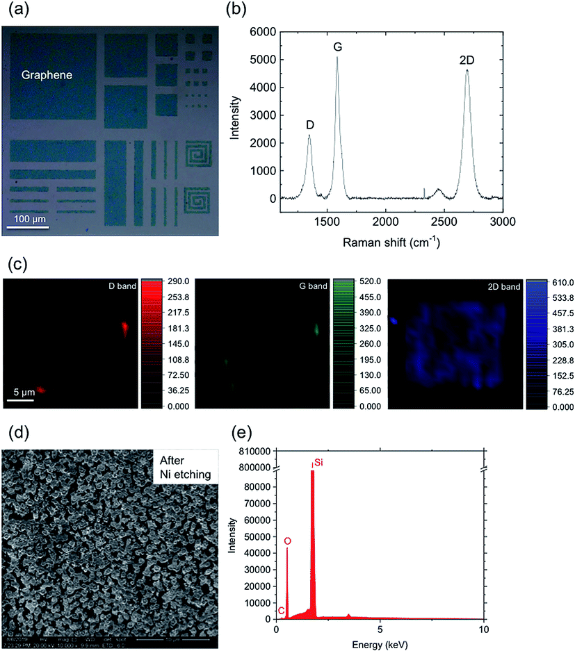 | ||
| Fig. 4 Optical microscope image (a), Raman spectrum (b) and the D, G, and 2D band Raman mapping images (c) and SEM (d) and EDX (e) results of the direct patterning graphene. EDX analysis revealed that the proportion of the number of C, O, Si, and Ni atoms of the direct patterning graphene is (in percentages) 2.44, 28.69, 68.86, and 0.02, respectively. | ||
As shown in Fig. 4(b), the three most pronounced peaks are the D peak at 1348 cm−1, the G peak at 1588 cm−1 and the 2D peak at 2695 cm−1. The I2D/IG intensity ratio is about 0.953 indicating that the graphene is bi-layered. The existence of the D band indicates that the graphene is again polycrystalline. Fig. 4(c) shows the D, G, and 2D band Raman mapping images obtained from a 20 μm × 20 μm square directly patterned graphene sample. The intensities of each of the Raman bands in the region are almost the same, indicating that the polycrystalline graphene is almost homogeneous as it happened for the sample shown in Fig. 2(c). We note that bright spots of D and G bands can be observed at the edge of the patterning graphene as shown in Fig. 4(c) (upper right and lower left edge of graphene). These bright spots in D and G bands might be caused by higher defects and higher thickness of graphene owing to sidewall and burr, and the disordered structure at the edge of the patterning graphene.44,45 In addition, SEM results (Fig. 4(d)) show that the round-shaped particles are not present in this case, and elements other than C, O, and Si were hardly observed during the EDX elemental analysis, as shown in Fig. 4(e). Thus, we found that the quality of the directly patterned graphene is nearly the same in the two cases. This graphene direct patterning procedure is advantageous in terms of reducing process complexity, steps, and cost because all the geometrical variables, position, size, and shape, are controllable by just performing the lithography process before the RTA process rather than doing a dry etch of the sample afterwards.
Light emitting applications of the direct patterning graphene
To test the viability of the directly patterned graphene for light emitting applications, Pd (145 nm)/Cr (5 nm) electrodes were deposited on the samples by vacuum vapor deposition as source and drain electrodes. The optical microscope image of the directly patterned graphene based light emitter is shown in Fig. 5(a). The size of the device graphene channels tested in this work was 5 μm length and 5 μm width.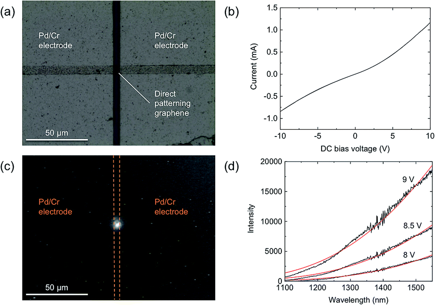 | ||
| Fig. 5 (a) Optical microscope image of the direct patterning graphene light emitter. (b) DC bias voltage (Vds) dependence of the current I (I–Vds curve). (c) IR camera image of the thermal emission at Vds = 9 V. (d) Emission spectra from the direct patterning graphene light emitter for Vds = 8–9 V with steps of 0.5 V. The red curves are the fitting results to Planck's law. | ||
The electrical and optical experiments were carried out at room temperature in a high-vacuum chamber. The DC bias voltage (Vds) dependence of the current I (I–Vds curve) was measured to evaluate the resistance characteristic (Fig. 5(b)). The I–Vds curve of the device exhibits almost Ohmic behavior in the probed Vds range and the resistivity at Vds = 9 V is 8914 Ω. The difference from perfect Ohmic behavior is believed to be caused by the metallicity of the small amount of residual Ni3C compounds on the substrate, which cannot be removed by the Ni etching process. The infrared emission was observed with an InGaAs CCD camera sensitive to wavelengths between 0.9 and 1.6 μm. Here, the emitted light was collected through the quartz optical window of the vacuum chamber and a microscope lens. A bright emission from the directly patterned graphene between the two electrodes is observed under DC bias voltage (Vds = 9 V) in vacuum. As shown in Fig. 5(c), the emission is highly localized in the graphene region. Fig. 5(d) shows the spectra of the light emitted by the graphene device. The broad spectra in the near IR region can be modelized with Planck's law,46 and the emission from the directly patterned graphene is considered blackbody radiation generated by Joule heating.7,8,11,14,16,47,48 The graphene temperatures, which are obtained by fitting Planck's law are estimated to be 748 K, 819 K and 920 K with Vds = 8 V, 8.5 V and 9 V, respectively. These findings demonstrate that a light emitting device based on direct patterning graphene operates on a par with light emitting devices based on high crystallinity graphene obtained by mechanical exfoliation method7,12,16,18 or CVD.7,11,17
Conclusions
In conclusion, we developed a growth procedure for graphene directly patterned on silicon substrates from a solid-state carbon source. In addition, we also developed a direct patterning procedure that allows us to achieve graphene samples with arbitrary position, size, and shape without the need to undergo dry etching steps. This enables a reduction of the process complexity, steps, and cost. Our procedure is divided into three main steps: lithography, rapid thermal annealing (RTA) and Ni etching. Noteworthy, during the lithography step, only a very thin film of metal catalyst Ni has to be deposited on top of the silicon substrate to strengthen the adhesion of the metal catalyst Ni and the solid carbon source a-C stacked films to the substrate. The Raman spectrum revealed that there are a few layers of polycrystalline graphene. The SEM, EDX, and XRD results revealed that the Ni etching process after the RTA process successfully removed the Ni-rich particles. Light emitting devices based on direct patterning graphene operate on a par with high crystallinity graphene based light emitting devices obtained by mechanical exfoliation method or CVD. Direct patterning graphene based light emitting devices integrated on silicon chips are expected to open new routes to the realization and commercialization of next-gen optical interconnects and silicon photonics. Moreover, applications are not limited to light emitting devices but can be extended to other optoelectronic devices such as photo-detectors and electronic device such as transistors, sensors, and circuits.Conflicts of interest
The authors declare no competing interests.Acknowledgements
The authors thank Dr E. Watanabe and Dr D. Tsuya of National Institute for Materials Science (NIMS) and Ms. S. Sugimoto of Keio University for their technical supports and fruitful discussions. This work was partially supported by a project of Kanagawa Institute of Industrial Science and Technology (KISTEC), PRESTO (Grant number JPMJPR152B) from JST, KAKENHI (Grant number 16H04355, 23686055 and 18K19025) and Core-to-Core program from JSPS, Spintronics Research Network of Japan, and NIMS Nanofabrication Platform in Nanotechnology Platform Project by MEXT.Notes and references
- J. A. Misewich, R. Martel, Ph. Avouris, J. C. Tsang, S. Heinze and J. Tersoff, Science, 2003, 300, 783 CrossRef CAS PubMed.
- S. Khasminskaya, F. Pyatkov, B. S. Flavel, W. H. Pernice and R. Krupke, Adv. Mater., 2014, 26, 3465 CrossRef CAS PubMed.
- T. Endo, J. I. Hayase and H. Maki, Appl. Phys. Lett., 2015, 106, 113106 CrossRef.
- Y. Liu, S. Wang, H. Liu and L. M. Peng, Nat. Commun., 2017, 8, 15649 CrossRef CAS PubMed.
- N. Hibino, S. Suzuki, H. Wakahara, Y. Kobayashi, T. Sato and H. Maki, ACS Nano, 2011, 5, 1215 CrossRef CAS PubMed.
- S. Khasminskaya, F. Pyatkov, K. Słowik, S. Ferrari, O. Kahl, V. Kovalyuk, P. Rath, A. Vetter, F. Hennrich, M. M. Kappes, G. Gol'tsman, A. Korneev, C. Rockstuhl, R. Krupke and W. H. P. Pernice, Nat. Photonics, 2016, 10, 727 CrossRef CAS.
- Y. Miyoshi, Y. Fukazawa, Y. Amasaka, R. Reckmann, T. Yokoi, K. Ishida, K. Kawahara, H. Ago and H. Maki, Nat. Commun., 2018, 9, 1279 CrossRef PubMed.
- T. Mori, Y. Yamauchi, S. Honda and H. Maki, Nano Lett., 2014, 14, 3277 CrossRef CAS PubMed.
- X. Gan, R. J. Shiue, Y. Gao, I. Meric, T. F. Heinz, K. Shepard, J. Hone, S. Assefa and D. Englund, Nat. Photonics, 2013, 7, 883 CrossRef CAS.
- F. Pyatkov, V. Fütterling, S. Khasminskaya, B. S. Flavel, F. Hennrich, M. M. Kappes, R. Krupke and W. H. P. Pernice, Nat. Photonics, 2016, 10, 420 CrossRef CAS.
- L. M. Lawton, N. H. Mahlmeister, I. J. Luxmoore and G. R. Nash, AIP Adv., 2014, 4, 087139 CrossRef.
- Y. D. Kim, H. Kim, Y. Cho, J. H. Ryoo, C. H. Park, P. Kim, Y. S. Kim, S. Lee, Y. Li, S. N. Park, Y. S. Yoo, D. Yoon, V. E. Dorgan, E. Pop, T. F. Heinz, J. Hone, S. H. Chun, H. Cheong, S. W. Lee, M. H. Bae and Y. D. Park, Nat. Nanotechnol., 2015, 10, 676 CrossRef CAS PubMed.
- P. Avouris, M. Freitag and V. Perebeinos, Nat. Photonics, 2008, 2, 341 CrossRef CAS.
- M. Fujiwara, D. Tsuya and H. Maki, Appl. Phys. Lett., 2013, 103, 143122 CrossRef.
- D. Liang and J. E. Bowers, Nat. Photonics, 2010, 4, 511 CrossRef CAS.
- M. Freitag, H. Y. Chiu, M. Steiner, V. Perebeinos and P. Avouris, Nat. Nanotechnol., 2010, 5, 497 CrossRef CAS PubMed.
- I. J. Luxmoore, C. Adlem, T. Poole, L. M. Lawton, N. H. Mahlmeister and G. R. Nash, Appl. Phys. Lett., 2013, 103, 131906 CrossRef.
- Y. D. Kim, Y. Gao, R. J. Shiue, L. Wang, O. B. Aslan, M. H. Bae, H. Kim, D. Seo, H. J. Choi, S. H. Kim, A. Nemilentsau, T. Low, C. Tan, D. K. Efetov, T. Taniguchi, K. Watanabe, K. L. Shepard, T. F. Heinz, D. Englund and J. Hone, Nano Lett., 2018, 18, 934 CrossRef CAS PubMed.
- K. S. Novoselov, A. K. Geim, S. V. Morozov, D. Jiang, Y. Zhang, S. V. Dubonos, I. V. Grigorieva and A. A. Firsov, Science, 2004, 306, 666 CrossRef CAS PubMed.
- Q. Yu, J. Lian, S. Siriponglert, H. Li, Y. P. Chen and S. S. Pei, Appl. Phys. Lett., 2008, 93, 113103 CrossRef.
- A. Reina, X. Jia, J. Ho, D. Nezich, H. Son, V. Bulovic, M. S. Dresselhaus and J. Kong, Nano Lett., 2009, 9, 30 CrossRef CAS PubMed.
- X. Li, W. Cai, J. An, S. Kim, J. Nah, D. Yang, R. Piner, A. Velamakanni, I. Jung, E. Tutuc, S. K. Banerjee, L. Colombo and R. S. Ruoff, Science, 2009, 324, 1312 CrossRef CAS PubMed.
- C. Mattevi, H. Kim and M. Chhowalla, J. Mater. Chem., 2011, 21, 3324 RSC.
- H. Ago, Y. Ogawa, M. Tsuji, S. Mizuno and H. Hibino, J. Phys. Chem. Lett., 2012, 3, 2228–2236 CrossRef CAS PubMed.
- Z. Sun, Z. Yan, J. Yao, E. Beitler, Y. Zhu and J. M. Tour, Nature, 2010, 468, 549 CrossRef CAS PubMed.
- J. Plutnar, M. Pumera and Z. Sofer, J. Mater. Chem. C, 2018, 6, 6082 RSC.
- J. Hofrichter, B. N. Szafranek, M. Otto, T. J. Echtermeyer, M. Baus, A. Majerus, V. Geringer, M. Ramsteiner and H. Kurz, Nano Lett., 2010, 10, 36 CrossRef CAS PubMed.
- Z. Yan, Z. Peng, Z. Sun, J. Yao, Y. Zhu, Z. Liu, P. M. Ajayan and J. M. Tour, ACS Nano, 2011, 5, 8187 CrossRef CAS PubMed.
- J. H. Chu, J. Kwak, T. Y. Kwon, S. D. Park, H. Go, S. Y. Kim, K. Park, S. Kang and S. Y. Kwon, ACS Appl. Mater. Interfaces, 2012, 4, 1777 CrossRef CAS PubMed.
- K. Banno, M. Mizuno, K. Fujita, T. Kubo, M. Miyoshi, T. Egawa and T. Soga, Appl. Phys. Lett., 2013, 103, 082112 CrossRef.
- G. Pan, B. Li, M. Heath, D. Horsell, M. L. Wears, L. A. Taan and S. Awan, Carbon, 2013, 65, 349 CrossRef CAS.
- W. Xiong, Y. S. Zhou, L. J. Jiang, A. Sarkar, M. M. Samani, Z. Q. Xie, Y. Gao, N. J. Ianno, L. Jiang and Y. F. Lu, Adv. Mater., 2013, 25, 630 CrossRef CAS PubMed.
- A. Delamoreanu, C. Rabot, C. Vallee and A. Zenasni, Carbon, 2014, 66, 48 CrossRef CAS.
- M. Miyoshi, M. Mizuno, Y. Arima, T. Kubo, T. Egawa and T. Soga, Appl. Phys. Lett., 2015, 107, 073102 CrossRef.
- W. Xiong, Y. S. Zhou, W. J. Hou, T. Guillemet, J. F. Silvain, Y. Gao, M. Lahaye, E. Lebraud, S. Xu, X. W. Wang, D. A. Cullen, K. L. More, L. Jiang and Y. F. Lu, RSC Adv., 2015, 5, 99037 RSC.
- M. Marchena, D. Janner, T. L. Chen, V. Finazzi and V. Pruneri, Opt. Mater. Express, 2016, 6, 2487 CrossRef CAS.
- J. Yamada, Y. Ueda, T. Maruyama and S. Naritsuka, Jpn. J. Appl. Phys., 2016, 55, 100302 CrossRef.
- L. Lu, J. T. M. D. Hosson and Y. Pei, Mater. Des., 2018, 144, 245 CrossRef CAS.
- R. N. Tiwari, M. Tripathi, M. Yoshimura and A. Kumar, Mater. Res. Bull., 2018, 107, 147 CrossRef CAS.
- V. P. Pham, H. S. Jang, D. Whang and J. Y. Choi, Chem. Soc. Rev., 2017, 46, 6276 RSC.
- A. C. Ferrari, J. C. Meyer, V. Scardaci, C. Casiraghi, M. Lazzeri, F. Mauri, S. Piscanec, D. Jiang, K. S. Novoselov, S. Roth and A. K. Geim, Phys. Rev. Lett., 2006, 97, 187401 CrossRef CAS PubMed.
- K. Yan, H. Peng, Y. Zhou, H. Li and Z. Liu, Nano Lett., 2011, 11, 1106 CrossRef CAS PubMed.
- M. A. Pimenta, G. Dresselhaus, M. S. Dresselhaus, L. G. Cançado, A. Jorio and R. Saito, Phys. Chem. Chem. Phys., 2007, 9, 1276 RSC.
- K. A. Jackson, Compound Semiconductor Devices Structures and Processing, Wiley-VCH, Weinheim, Germany, 1998 Search PubMed.
- C. Casiraghi, A. Hartschuh, H. Qian, S. Piscanec, C. Georgi, A. Fasoli, K. S. Novoselov, D. M. Basko and A. C. Ferrari, Nano Lett., 2009, 9, 1433 CrossRef CAS PubMed.
- M. Planck, Ann. Phys., 1901, 4, 553 CrossRef.
- H. R. Barnard, E. Zossimova, N. H. Mahlmeister, L. M. Lawton, I. J. Luxmoore and G. R. Nash, Appl. Phys. Lett., 2016, 108, 131110 CrossRef.
- M. H. Bae, Z. Y. Ong, D. Estrada and E. Pop, Nano Lett., 2010, 10, 4787 CrossRef CAS PubMed.
| This journal is © The Royal Society of Chemistry 2019 |