
 Open Access Article
 This Open Access Article is licensed under a Creative Commons Attribution-Non Commercial 3.0 Unported Licence
Formation of submicron-sized silica patterns on flexible polymer substrates based on vacuum ultraviolet photo-oxidation†
Cheng-Tse
Wu
 a,
Ahmed I. A.
Soliman
ab,
Toru
Utsunomiya
a,
Takashi
Ichii
a and
Hiroyuki
Sugimura
*a
a,
Ahmed I. A.
Soliman
ab,
Toru
Utsunomiya
a,
Takashi
Ichii
a and
Hiroyuki
Sugimura
*a
aDepartment of Materials Science and Engineering, Graduate School of Engineering, Kyoto University, Kyoto 606-8501, Japan. E-mail: sugimura.hiroyuki.7m@kyoto-u.ac.jp; Tel: +81-75-753-9131
bChemistry Department, Faculty of Science, Assiut University, Assiut 71516, Egypt
First published on 10th October 2019
Abstract
Formation of precise and high-resolution silica micropatterns on polymer substrates is of importance in surface structuring for flexible device fabrication of optics, microelectronic, and biotechnology. To achieve that, substrates modified with affinity-patterns serve as a strategy for site-selective deposition. In the present paper, vacuum ultraviolet (VUV) treatment is utilized to achieve spatially-controlled surface functionalization on a cyclo-olefin polymer (COP) substrate. An organosilane, 2,4,6,8-tetramethylcyclotetrasiloxane (TMCTS), preferentially deposits on the functionalized regions. Well-defined patterns of TMCTS are formed with a minimum feature of ∼500 nm. The secondary VUV/(O)-treatment converts TMCTS into SiOx, meanwhile etches the bare COP surface, forming patterned SiOx/COP microstructures with an average height of ∼150 nm. The resulting SiOx patterns retain a good copy of TMCTS patterns, which are also consistent with the patterns of photomask used in polymer affinity-patterning. The high quality SiOx patterns are of interests in microdevice fabrication, and the hydrophilicity contrast and adjustable heights reveal their potential application as a “stamp” for microcontact printing (μCP) techniques.
Introduction
Flexible functional devices based on polymer substrates have attracted much attention for their great potential applications.1–3 Various oxide films have been formed on polymer substrates to achieve their functionality.4–7 In particular, patterning of oxide thin films is of great significance in the development of sensor arrays,8 memory arrays,9 integrated electronics,10 solar cell,11 and so forth. In general, the formation for such oxide thin films should be conducted in mild conditions to remain the optical and mechanical properties of polymer substrate, therefore, the traditional micropatterning strategies involving erosive chemicals or high temperature conditions are no longer favoured.7,12,13Silica micron/submicron-sized patterns were reported to be fabricated on substrates for the application in patterning techniques,13,14 optics,15,16 optoelectronics,17 microelectronics,18 sensors,19 and biotechnology.20,21 A top-down approach for the silica patterning applicable to arbitrary substrates was reported, which sputtered silica films onto photoresist-patterned surface.21 Other approaches involving bottom-up techniques were reported, in which the use of photoresist was not required.20,22,23 A poly(dimethylsiloxane) (PDMS) with desired shapes was attached onto the surface to build a “microchannel”, subsequently a silica precursor was then injected into the PDMS channel and selectively deposited on the substrates.20 Although this site-selective silica treatment was applicable to various substrates, non-continuous patterns such as dotted patterns could not be achieved by this mean.
Site-selective oxide deposition was reported as a useful technique for patterning oxides on substrates, and the achievable shapes and resolution were related to the photomask. Patterns of SiOx (ref. 22) and TiO2 (ref. 24) were successfully prepared on silicon substrates via the assistance of self-assembled monolayers (SAM). SAM-covered silicon substrates were patterned by UV irradiation with a photomask, causing an affinity contrast between the UV-treated and non-treated regions. The oxide deposits could thus selectively grow guided by the affinity-patterns. In contrast, polymer substrates are commonly known as non-polar or poorly polar materials which have quite “inert” surface for the deposition of oxide layers. To achieve an affinity-pattern for site-selective deposition, several photochemical treatments could be used to tailor the surface of polymer substrates.25–27 A famous example was given, which applied a UV-activated oxidation to arbitrary polymer substrates in an ammonium persulfate (APS) solution.27 The sulfate anion groups (–OSO3−) were implanted on the outermost surface of the polymer substrates, resulting in the increase of hydrophilicity. The spatial-controlled hydrophilic treatment was successfully conducted by UV irradiation through a photomask. The affinity-patterned polymer surface was used for the selective deposition of SiOx,13 TiO2 (ref. 28) and ZnO.29 However, the affinity-patterning from this technique was conducted in liquid phase, in which the excitation UV light might be refracted to cause inconsistency, and photoexcited APS molecules in the bulk liquid might lead to a broadening of oxidized area, which constrained the achievable resolution. Moreover, the photoactive chemicals were required for such surface-tailoring techniques, which caused complexity in operation, and also generated chemical wastes. Therefore, a dry method, which does not require oxidative chemical reagents, is considered to be an alternative oxidation methodology.
VUV (λ = 172 nm, Xe2 excimer lamp) light is strongly absorbed by O2, generating active species such as ozone and atomic oxygen.30–33 VUV light and the active oxygen species (VUV/(O)) are highly oxidative to organics.7 Such VUV/(O)-treatment is widely used in photo-oxidation including the removal of organics and the surface hydrophilic treatment.25,30,31 Polar functional groups (CHO, CH2OH, COOH, etc.) could thus be decorated onto a cyclo-olefin polymer (COP) substrate.25 These Polar functional groups favoured the oxide depositions since they could participate in the condensation polymerization of sol–gel depositions.34,35 Moreover, the VUV/(O)-generated functional groups were reported to be good reaction sites for the silanization.36–38 Thin films of an organosilane – 2,4,6,8-tetramethylcyclotetrasiloxane (TMCTS) were fabricated on the VUV/(O)-treated polymer substrates.36,37 The TMCTS thin films were further converted into SiOx by the secondary VUV/(O)-irradiation.36–38 The resulting SiOx layers were flat and strongly attached on the polymer surface due to the chemical bonding. Inspired by the above studies, we expect a precise and high-resolution TMCTS patterning on the VUV/(O)-patterned COP substrate. The secondary VUV/(O)-irradiation converts the TMCTS patterns to SiOx patterns.
In this study, we demonstrated submicron-sized SiOx patterns on the COP substrates by VUV/(O)-treatments (Fig. 1). In the first part, we introduced a VUV/(O)-treatment for spatially-controlled surface modification on COP surface. In the second part, adsorption of TMCTS on the pristine or VUV/(O)-modified COP surface was investigated by Fourier transform infrared spectroscopy (FTIR). Photo-oxidation converting TMCTS into SiOx was studied by using FTIR and X-ray photoelectron spectroscopy (XPS). In the last part, site-selective deposition of TMCTS was conducted. Formation of TMCTS patterns on the affinity-patterned COP substrates was observed by scanning electron microscope (SEM). After the secondary VUV/(O)-treatment, the TMCTS patterns were converted into silica patterns.
 | ||
| Fig. 1 Schematic illustration of (a) VUV/(O)-modification on COP surface, (b) TMCTS deposition on the modified COP surface, (c) SiOx thin films formed by VUV/(O)-photo-oxidation, (d) affinity-patterning by VUV/(O)-treatment through a photomask, (e) site-selective deposition of TMCTS on the affinity-patterned COP surface, (f) SiOx microstructures on the COP substrate. | ||
Experimental
VUV/(O)-patterning on COP
VUV/(O)-treatment was conducted using VUV light (λ = 172 nm) from a Xe2 excimer lamp (UER 20–172 V, Ushio Inc.). The power of VUV light was measured as 10 mW cm−2 with N2 purging at a distance of 5 mm from the window of VUV lamp. All the VUV/(O)-treatments were carried out at this distance. A cyclo-olefin polymer (COP, ZF16-188, ZeonorFilm®, ZEON Corporation) sheet with a thickness of 0.188 mm was cut into the size of 2 cm × 2 cm for the use as a substrate. The protective films on the COP substrates were peeled off, then the newly exposed COP surface was VUV/(O)-treated under 103 Pa dried air environment for 10 min. The VUV/(O)-generated functional groups were characterized by attenuated total reflectance FTIR (ATR-FTIR).The affinity-patterning on the COP substrate was performed by VUV/(O)-treatment through a photomask. The photomask consists of a 100 nm-thick chromium coating with patterns on a 2 mm-thick quartz plate (93% transparency for light at 172 nm). After affinity-patterning, the changes in topography and phase were measured by AFM with AC-mode.
TMCTS-treatment and silica thin film formation
The procedure of TMCTS-treatment was described as below. A precursor solution was prepared by mixing 2,4,6,8-tetramethylcyclotetrasiloxane (TMCTS, 99%, Alfa-Aesar), ethanol (99.5%, Nacalai Tesque), and ultrapure water (resistivity of 18.2 MΩ cm) in the amount of 5 mL, 10 mL, 0.1 mL, respectively. The COP substrates were located with the precursor solution in a 120 cm3 perfluoroalkoxy alkane jar (PFA jar, ARAM Corporation) and heated in an oven maintaining the temperature at 80 °C for 24 hours. The physically adsorbed precursor molecules were washed away through the ultrasonic cleaning in ethanol for 1 hour. The resulting TMCTS thin films were further treated by VUV/(O) under 103 Pa dried air environment for a series of irradiation time. The characterization of TMCTS thin films before and after VUV/(O)-treatment was conducted by WCA measurement, XPS and ATR-FTIR.Site-selective TMCTS deposition on affinity-patterns
TMCTS-treatment was applied on the affinity-patterned COP substrates, which were prepared as previously described. After the TMCTS-treatment, the substrates were ultrasonically cleaned in ethanol for 1 hour to leave a TMCTS pattern. Scanning electron microscope (SEM) equipped with an energy dispersive X-ray spectroscopy (EDX) was used to study the site-selective adsorption of TMCTS. Afterwards, the TMCTS patterns were further treated by VUV/(O) to form SiOx micro arrays.Analytical techniques
XPS measurement was performed using a photoelectron spectrometer (ESCA-3400 system, Kratos Analytical) equipped with Mg Kα X-ray source (emission current 10 mA, accelerate voltage 10 kV) to investigate the chemical changes of COP surface during the VUV/(O)-treatment and TMCTS adsorption. High resolution spectra were observed at C 1s and Si 2p regions with each energy step of 0.1 eV. The obtained XPS spectra were referenced to C–C (285.0 eV) of C 1s spectra. FTIR (Excalibur FTS-3000, Digilab) was used to identify the formation of VUV/(O)-generated functional groups and the adsorption of organosilane, which could support the results of XPS. The IR measurement was conducted in ATR-mode using a germanium ATR crystal (GATR, Harrick Scientific Product) with a reflection angle of 65°. The IR spectra were received in the range of 2300–900 cm−1 with a resolution of 2 cm−1. WCA values were obtained with a static contact angle meter (DM 500, Kyowa Interface Science Co. Ltd.), where the volume of water droplet was fixed at 1.8 μL. SEM (S–3500H, Hitachi) and EDX (Delta Plus 3, Kevex/Fisons Instruments Inc.) were used for observing the TMCTS patterns and specifying the existence of silicon element. The SEM images and EDX area analysis were obtained with an electron beam acceleration voltage of 5 kV. AFM (MFP-3D, Oxford Instruments) was conducted to visualize the morphology of the TMCTS and silica micropatterns. The images of topography and phase were acquired by AC-mode using aluminium backside coated Si probes (SI-DF-40, Hitachi Hi-Tech Co. Ltd.).Results and discussion
VUV/(O)-modification on COP surface
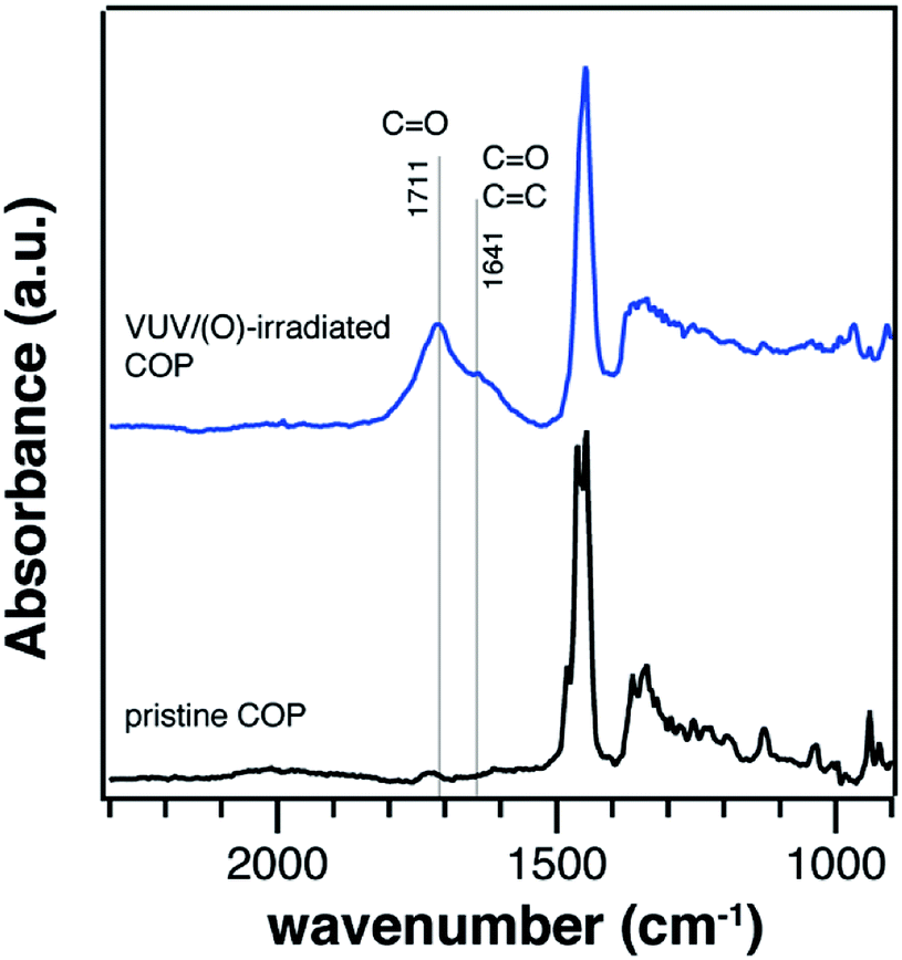
ATR-FTIR measurement were conducted to verify the surface modification on the COP substrates, as shown in Fig. 2. A band in 1500–1400 cm−1 with two split peaks at 1464 cm−1 and 1447 cm−1 could be attributed to CH2 deformation vibrations.25,26 VUV/(O)-treatment introduced absorption bands in the frequency range of 1800–1600 cm−1, which was attributed to carbonyl groups (C![[double bond, length as m-dash]](https://www.rsc.org/images/entities/char_e001.gif) O).25,26 An appearance of absorption bands at 1800–1500 cm−1 contained doublet structure, where the sharper peak was centred at 1711 cm−1 and the broad band was centred at 1641 cm−1. The sub-peak centred at 1711 cm−1 could be attributed to CO vibrations from aliphatic ketones, aldehydes, and carboxylic acid species, which were resulted from the oxidation of alkyl groups.25,31 A broad absorption band at 1641 cm−1 could be attributed to CO from unsaturated ketones and aldehydes, as well as CC of alkene structure.25 These unsaturated structures could be attributed to the ring opening reaction and dehydrogeneration.25,26 Based on these results, the generation of functional groups on COP surface was confirmed. These polar functional groups are thought to be of importance for the deposition of oxides and silanes.
O).25,26 An appearance of absorption bands at 1800–1500 cm−1 contained doublet structure, where the sharper peak was centred at 1711 cm−1 and the broad band was centred at 1641 cm−1. The sub-peak centred at 1711 cm−1 could be attributed to CO vibrations from aliphatic ketones, aldehydes, and carboxylic acid species, which were resulted from the oxidation of alkyl groups.25,31 A broad absorption band at 1641 cm−1 could be attributed to CO from unsaturated ketones and aldehydes, as well as CC of alkene structure.25 These unsaturated structures could be attributed to the ring opening reaction and dehydrogeneration.25,26 Based on these results, the generation of functional groups on COP surface was confirmed. These polar functional groups are thought to be of importance for the deposition of oxides and silanes.
 | ||
| Fig. 2 ATR-FTIR spectra of COP before and after VUV/(O)-irradiation for 10 min. | ||
In this section, we demonstrated that the photochemical modification by VUV/(O)-treatment is effective in obtaining hydrophilicity at the surface. Since the surface modification is induced by VUV/(O)-treatment, patterned surface modification could be achieved through a photomask. By this mean, we expect that the confined surface tailoring and further site-selective nano-architecture could be realized.
Affinity-patterning was performed on COP substrates by applying VUV/(O)-treatment through a photomask with circular patterns. The VUV photons penetrated through the slits and irradiated the COP surface, simultaneously the active oxygen species were generated above the irradiated regions. The dispersion of the active oxygen species was reported to affect the masked regions as well, leading to a slight broadening of oxidized area.39 Here, the changes of topography and phase during affinity-patterning were observed by AFM, as shown in Fig. 3. In the first 1 min VUV/(O)-irradiation through a photomask, the differences between VUV/(O)-irradiated regions and masked regions were clearly identified by the topographic image (Fig. 3a) and phase image (Fig. 3b). The phase image portrays the mapping of mechanical properties on the surface. The phase image (Fig. 3b) shows a distinct difference in mechanical properties between the VUV/(O)-irradiated and the masked regions. In the topographic image (Fig. 3a), the VUV/(O)-irradiated regions were found to be higher than the masked regions, most likely due to the permeation of oxygen into COP and the generation of oxygenated carbon groups. On the other hand, VUV/(O) is known to etch the irradiated region via photo-degradation of COP.26 After 10 min VUV/(O)-irradiation through a photomask, the differences in surface properties can be still observed in phase image (Fig. 3d), and the COP surface turned into topographically flat (Fig. 3c). Thus, the affinity-patterned COP substrate with little topographic difference was obtained.
 | ||
| Fig. 3 AFM topographic images of VUV/(O) affinity-patterning on COP surface for (a) 1 min and (c) 10 min, respectively. (b) and (d) are corresponding phase images. | ||
TMCTS thin films and photo-oxidation
The polar functional groups on the COP surface were reported to play a role in the organosilane adsorption since they provide chemical anchoring sites for silanization.36,37,40 In Fig. 4, the ATR-FTIR spectra portray the evolution of IR absorption bands after TMCTS-treatments on the pristine COP or VUV/(O)-modified COP substrates. No obvious change was found before (Fig. 4A) and after (Fig. 4B) the TMCTS-treatment applied on the pristine COP substrate. In comparison, several newly generated peaks were found after TMCTS-treatments applied on the VUV/(O)-modified COP substrate, which were shown in Fig. 4C and D. The COP related IR bands were also detected since the sampling depth can reach to 0.37–0.47 μm in region of 1800–1400 cm−1.41 Absorption bands at 2168 cm−1 and 1270 cm−1 corresponded to Si–H stretching vibration and Si–CH3 deformation, respectively.42–44 A broad absorption band at 1160–975 cm−1 was due to Si–O–Si asymmetric stretching vibrations. Compared with the IR spectra of TMCTS monomer (Fig. S2†), the obtained TMCTS coatings revealed a broader frequency range of Si–O–Si vibration. This broad frequency range could consist of vibrational modes from intact TMCTS rings at 1113 cm−1 and 1090 cm−1, and silica-like structure with different Si–O–Si bond angles.43–47 | ||
| Fig. 4 ATR-FTIR spectra of modified COP surfaces. (A) Pristine COP, (B) pristine COP after TMCTS-treatment, (C) 10 min VUV/(O)-modified COP, and (D) 10 min VUV/(O)-modified COP after TMCTS-treatment. | ||
Based on the IR results, two phenomenon were clarified: (1) the VUV/(O)-modification on the COP surface was crucially important for the further silanization. (2) The broader frequency range of Si–O–Si asymmetric stretching vibration suggested that the intermolecular linkages incorporated in the TMCTS layers on the COP surface, forming the primary Si–O–Si network with siloxane structures.
TMCTS thin films were known to be converted into inorganic SiOx thin films after VUV/(O)-treatments, where VUV/(O) caused the removal of the methyl terminal groups and formed the network of Si–O–Si bond chains.36,37 Our chemically adsorbed TMCTS thin films on the COP surface were treated by VUV/(O) for variant irradiation time. XPS and ATR-FTIR measurements were conducted to elucidate the changes of VUV/(O)-treated TMCTS films, as shown in Fig. 5. The XPS C 1s and Si 2p spectra were shown in Fig. 5a. The intensity of C 1s decreased with the irradiation time. After 50 min VUV/(O)-treatment, the atomic ratio of carbon decreased from 0.60 to 0.12. This remnant of carbon is commonly attributed to contaminant adsorption from the atmospheric environment.48,49 In Si 2p spectra, the peak position was gradually shifted from 103.0 eV to 103.9 eV. This chemical shift is usually attributed to the chemical conversion from organosilane to amorphous silica.36,42 The atomic concentration was also calculated based on the Si 2p and O 1s spectra. The atomic ratio of Si to O was calculated to be 1![[thin space (1/6-em)]](https://www.rsc.org/images/entities/char_2009.gif) :2.7, which is in good agreement with previously reported SiOx depositions.13,36 ATR-FTIR measurements were also performed to understand the evolution of Si-related bonds, as shown in Fig. 5b. After the first 1 min irradiation, the IR band due to stretching vibration of Si–H (∼2176 cm−1) vanished. A reduction of band related to Si–CH3 was also observed. VUV/(O)-treatment was further conducted in longer irradiation time. The peak of Si–CH3 was largely reduced. The Si–O–Si asymmetric stretching bands, which are in the range of 1160–975 cm−1, were gradually sharpen to 1070 cm−1. This vibration at 1070 cm−1 and another newly generated vibration at 1229 cm− 1 are commonly attributed to Si–O–Si vibrations in silica, which were denoted as transverse optical mode (TO)43,50 and longitudinal optical vibration mode (LO),50–52 respectively. A sub-peak at 1126 cm−1 was also observed. This peak can be attributed to Si–O–Si of caged structures, which are similar to the structures in silsesquioxane polymers.45,47 The results from XPS and ATR-FTIR indicate that the methyl groups in TMCTS layers were clearly removed, and the –Si–O–Si– chains were converted into fully relaxed silica network.
:2.7, which is in good agreement with previously reported SiOx depositions.13,36 ATR-FTIR measurements were also performed to understand the evolution of Si-related bonds, as shown in Fig. 5b. After the first 1 min irradiation, the IR band due to stretching vibration of Si–H (∼2176 cm−1) vanished. A reduction of band related to Si–CH3 was also observed. VUV/(O)-treatment was further conducted in longer irradiation time. The peak of Si–CH3 was largely reduced. The Si–O–Si asymmetric stretching bands, which are in the range of 1160–975 cm−1, were gradually sharpen to 1070 cm−1. This vibration at 1070 cm−1 and another newly generated vibration at 1229 cm− 1 are commonly attributed to Si–O–Si vibrations in silica, which were denoted as transverse optical mode (TO)43,50 and longitudinal optical vibration mode (LO),50–52 respectively. A sub-peak at 1126 cm−1 was also observed. This peak can be attributed to Si–O–Si of caged structures, which are similar to the structures in silsesquioxane polymers.45,47 The results from XPS and ATR-FTIR indicate that the methyl groups in TMCTS layers were clearly removed, and the –Si–O–Si– chains were converted into fully relaxed silica network.
 | ||
| Fig. 5 (a) XPS C1s and Si 2p spectra of TMCTS thin films before and after VUV/(O)-treatment for 1, 5, 10, 50 min. (b) ATR-FTIR spectra of TMCTS before and after VUV/(O)-treatment for 1, 5, 10, 50 min (from bottom to top). | ||
Until here, we successfully formed inorganic thin films – SiOx on the COP surface. The static water contact angles (WCA) were also measured for evaluating the surface change. WCA values of (a) pristine COP surface, (b) VUV/(O)-modified COP, adsorbed TMCTS thin films (c) before and (d) after VUV/(O)-treatment were shown in Fig. 6. After 10 min VUV/(O)-treatment on pristine COP, the WCA values decreased from 96.7° to 24.3° (Fig. 6a and b). This modified surface provided sufficient chemical affinity for silanization of TMCTS molecules, which resulted in a good coverage of organosilane thin films. The WCA value of resulting TMCTS thin films was measured to be 95.9° (Fig. 6c), which is consistent with other reported TMCTS depositions from CVD techniques.36,37,53 The increased hydrophobicity is due to the terminal CH3 groups toward the outer surface.37,42,53 By the secondary VUV/(O)-treatment, the organic moieties were eliminated, resulting in a hydrophilic inorganic surface (Fig. 6d).
 | ||
| Fig. 6 WCA images and values of (a) pristine COP, (b) VUV/(O)-modified COP, (c) TMCTS thin films and (d) VUV/(O)-treated TMCTS thin films. | ||
Site-selective silanization on affinity-patterns
The pristine COP surface was found to be chemically inert for the silanization. On the contrary, TMCTS thin films were successfully formed on the VUV/(O)-modified COP substrate due to the polar functional groups. Based on these, we expected that TMCTS molecules could selectively deposit at VUV/(O)-modified regions on COP surface. TMCTS-treatment was carried out on the COP substrates with affinity-patterns. The selective depositions were monitored by SEM-EDX (Fig. 7) and AFM (Fig. 8) analysis. | ||
| Fig. 7 SEM-EDX analysis of TMCTS patterns on COP surface. (a) SEM image illustrates the patterned regions, marked as Area 1 and Area 2. (b) Area EDX analysis of corresponding position in the SEM image. Line patterns of various features in (c) domains, which have (interval, line width) of (1 μm, 0.5 μm) and (4 μm, 0.5 μm). (d) Domains, which have (interval, line width) of (2 μm, 0.5 μm) and (2 μm, 1 μm). | ||
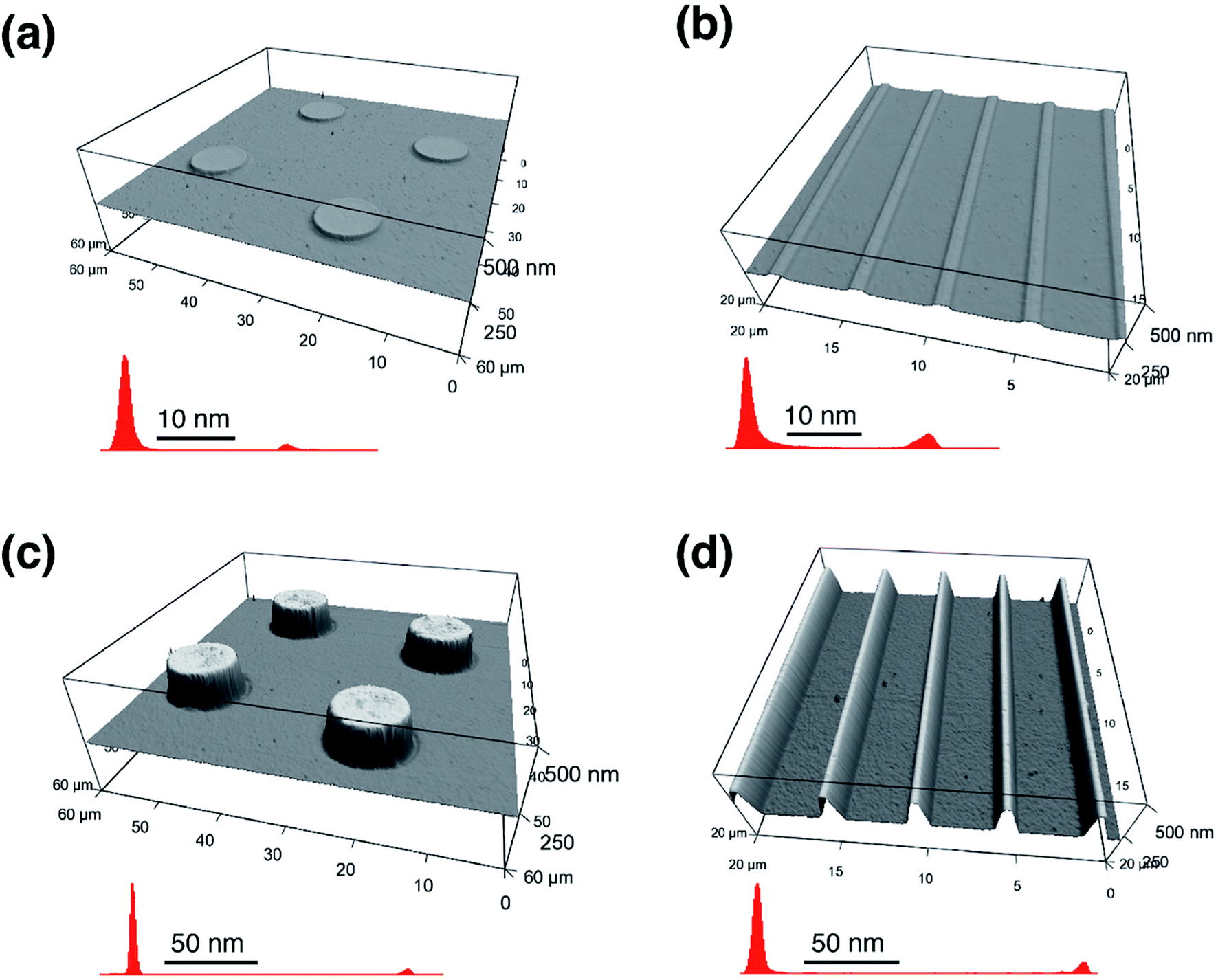 | ||
| Fig. 8 AFM 3D-topographic images and the corresponding height histogram of TMCTS patterns (a and b) before and (c and d) after VUV/(O)-treatment for 50 min, where (a and c) represent the circular pattern, and (b and d) represent the line pattern. | ||
In Fig. 7a, the SEM image illustrates a micro array in circular shapes, as indicated by the white arrow. This contrast is probably due to the difference in height from the selective deposition of TMCTS molecules. The height measurement was also made by AFM, which will be described later. EDX analysis was conducted to elucidate the elements in the circular patterns (Area 1) and out of the circular patterns (Area 2). In Fig. 7b, the upper panel illustrates the EDX spectra in Area 1, which represent the corresponding position in the SEM image. A peak at ∼1.74 keV was observed. This position is attributed to Si Kα X-ray line. In contrast, the lower panel illustrating the EDX spectra of Area 2 revealed only noises near the position of Si Kα X-ray line. It is suggested that TMCTS with the Si element deposited selectively in the circular-shaped regions, which matched the hydrophilic regions of the affinity-patterned COP surface. In Fig. 7c and d, high-resolution TMCTS line patterns were also performed on the COP surface with line-shaped hydrophilic patterns.
The TMCTS-micropatterned substrates were further treated by VUV/(O) to convert TMCTS to SiOx. The morphology and height histogram of TMCTS micropatterns before and after VUV/(O)-treatment are shown in Fig. 8. The height of the TMCTS micropatterns is ∼20 nm by the height histogram. After VUV/(O)-treatment, TMCTS patterns were converted to SiOx patterns. The thickness of TMCTS films is thought to be reduced after VUV/(O)-treatment due to the removal of organic parts and the condensation of silica structures.22,36,37,43 However, the bare COP surface was etched since VUV/(O) caused the degradation of COP, as previously reported.25,26 On the other hand, the regions covered by TMCTS (later converted to SiOx) were protected from the photo-degradation since the active oxygen species cannot reach the masked COP. Although a few amounts of the VUV photons could penetrate the SiOx layers and might dissociate the C–O–Si bonds, the exfoliation of silica thin films from COP was not found in the previously demonstrated XPS and FTIR results, which is also in good agreement with previously reported silica thin films.36,37 Therefore, the silica micro arrays with COP pillar-like supports were fabricated. The average height of the microstructures of SiOx/COP pillars is ∼150 nm obtained from the height histogram. Since the TMCTS adsorptions were strictly confined in the affinity-patterned regions, and SiOx-masked COP was not changed by the further VUV/(O)-treatment, the shapes of the micropatterns remained consistent with affinity-patterned regions even after the secondary VUV/(O)-treatment.
The optical micrographs show that high quality SiOx/COP micro arrays on the flexible substrates were successfully fabricated over a large area, as shown in Fig. 9. The SiOx micropatterns are in good agreement with the slit size of the photomask used in the affinity-patterning. High-resolution SiOx micro arrays fabricated on flexible substrates are of great importance for the design and creation of flexible microdevices in optics, electronics, optoelectronics and biotechnology, which were mentioned in the introduction. Since the resolution is achievable in sub-μm scale, the resulting patterns have great potential in future formation of metamaterials.54 Furthermore, our silica-patterned polymer substrates might be devoted to further patterning techniques. There is a distinct height difference between SiOx and the COP substrate. This enables us to transfer ink films onto SiOx patterns without contaminating the COP substrate. By dipping the silica-patterned polymer substrates to the (3-aminopropyl)triethoxysilane (APTES) gel films, APTES is immobilized on silica patterns with Si–O–Si linkage to form APTES patterns, which are useful in patterning of proteins.13 Similar process can be conducted by transferring metal oxide precursor to silica patterns for the direct formation of metal oxide patterns, which should receive great interest of electronic device fabrication on flexible polymer substrates.29 Another potential application is to use the SiOx micropatterned COP as a “stamp” for the micro contact printing (μCP) techniques. Recently, μCP techniques have been used for micropatterning of various inks, which commonly use poly(dimethylsiloxane) (PDMS) as a “stamp”.55 However, previous studies reported that PDMS cannot fulfil the requirement of printing polar inks and proteins due to its hydrophobicity.56–59 PDMS stamps could be easily hydrophilized by oxygen plasma, however, the effect of the hydrophilization is only temporary, which means the stamps should be hydrophilized every-time prior to the usage. Moreover, PDMS has a number of drawbacks due to its softness such as limitation of pattern shapes and resolution.60 Therefore, our SiOx-patterned COP can be a potential candidate for the future μCP “stamp” since it can be easily patterned, has tuneable height difference, and has longer-life hydrophilicity contrast.
 | ||
| Fig. 9 Optical micrographs of resulting silica micro arrays. The circular patterns with a diameter of 10 μm are shown by (a) bright field image and (b) dark field image. The line patterns with (interval, line width) of (4 μm, 0.5 μm) are shown by (c) bright field image and (d) dark field image. | ||
Our VUV/(O) affinity-patterning technique is a powerful method, which can provide the templates with an affinity contrast for the further patterning. Without the requirement of photo-active chemicals for oxidation, our method is simple and environmental-friendly. This mild and highly precise treatment showed its application to patterning of silanes and SiOx on the COP substrates, and for sure it can be extended to various polymer substrates. A wide range of silanes and semiconductors can be patterned on the VUV/(O)-modified polymer substrates through the design of site-selective deposition. We believe that our method is of great interests for future microfabrication.
Conclusions
We demonstrated a confined micropatterning of SiOx on COP substrate via two steps VUV/(O)-treatment. First, VUV/(O)-treatment was experimentally proved to introduce hydrophilic functional groups onto the COP surface. An affinity-patterned COP substrate was prepared by VUV/(O)-treatment through a photomask. TMCTS molecules were chemically adsorbed on the COP substrate by a condensation reaction between the silanol groups and photo-chemically modified COP surface. The resulting siloxane linkages were found to be strong against ultra-sonication. The secondary VUV/(O)-treatment converted TMCTS into SiOx. On the affinity-patterned COP, TMCTS molecules preferentially deposited at the VUV/(O)-modified regions, forming TMCTS micron/submicron-sized patterns with a good fidelity to the photomask. The secondary VUV/(O)-treatment converted the TMCTS patterns into SiOx patterns, and the bare part of COP surface was etched to a depth of ∼150 nm. High-quality SiOx patterns formed on polymer substrates are of great interests for flexible microdevices. Since the resolution is achievable in sub-μm scale, our SiOx patterns have great potential in future formation of metamaterials. Moreover, the SiOx microstructures have a distinct contrast in heights and hydrophilicity, revealing their possible applications in μCP techniques. Our VUV/(O)-patterning technique and the resulting SiOx micron/submicron-sized arrays have great potential applications to patterning techniques and microdevice fabrication for optics, microelectronics, sensors and biotechnology.Conflicts of interest
There are no conflicts to declare.Acknowledgements
This work was partially supported by JSPS KAKENHI grant number JP15H02297. Cheng-Tse Wu acknowledges the Japan-Taiwan Exchange Association for financial support.Notes and references
- Y. Liu, K. He, G. Chen, W. R. Leow and X. Chen, Chem. Rev., 2017, 117, 12893–12941 CrossRef CAS.
- S. Park, G. Wang, B. Cho, Y. Kim, S. Song, Y. Ji, M. Yoon and T. Lee, Nat. Nanotechnol., 2012, 7, 438–442 CrossRef CAS.
- J. S. Discrete, K. Nomura, H. Ohta, A. Takagi and T. Kamiya, Nature, 2004, 432, 3383–3386 Search PubMed.
- Y. H. Kim, J. S. Heo, T. H. Kim, S. Park, M. H. Yoon, J. Kim, M. S. Oh, G. R. Yi, Y. Y. Noh and S. K. Park, Nature, 2012, 489, 128–132 CrossRef CAS PubMed.
- B. K. Song, J. Noh, T. Jun, Y. Jung, H. Kang and J. Moon, Adv. Mater., 2010, 22, 4308–4312 CrossRef.
- J. Wang, W. Weng, M. Tsai, M. Lee, S. Horng, T. Perng, C. Kei, C. Yu and H. Meng, J. Mater. Chem., 2010, 20, 862–866 RSC.
- P. C. With, U. Helmstedt, S. Naumov, A. Sobottka, A. Prager, U. Decker, R. Heller, B. Abel and L. Prager, Chem. Mater., 2016, 28, 7715–7724 CrossRef CAS.
- S. Bai, W. Wu, Y. Qin, N. Cui, D. J. Bayerl and X. Wang, Adv. Funct. Mater., 2011, 21, 4464–4469 CrossRef CAS.
- S. Kim, H. Y. Jeong, S. K. Kim, S. Choi and K. J. Lee, Nano Lett., 2011, 11, 5438–5442 CrossRef CAS.
- Y. S. Rim, H. Chen, Y. Liu, S. H. Bae, H. J. Kim and Y. Yang, ACS Nano, 2014, 8, 9680–9686 CrossRef CAS.
- A. Narazaki, Y. Kawaguchi, H. Niino, M. Shojiya, H. Koyo and K. Tsunetomo, Chem. Mater., 2005, 17, 6651–6655 CrossRef CAS.
- U. Schulz and N. Kaiser, Prog. Surf. Sci., 2006, 81, 387–401 CrossRef CAS.
- S. Gan, P. Yang and W. Yang, Sci. China: Chem., 2010, 53, 173–182 CrossRef CAS.
- R. H. Jin and J. J. Yuan, Adv. Mater., 2009, 21, 3750–3753 CrossRef CAS.
- X. Ding, Y. Kawaguchi, T. Sato, A. Narazaki, R. Kurosaki and H. Niino, J. Photochem. Photobiol., A, 2004, 166, 129–133 CrossRef CAS.
- H. Ikeda, S. Fujino and T. Kajiwara, J. Am. Ceram. Soc., 2011, 94, 2319–2322 CrossRef CAS.
- K. Q. Le, M. Nixon and J. Bai, IEEE Journal of Photovoltaics, 2015, 5, 1125–1129 Search PubMed.
- S. Y. Chou, C. Keimel and J. Gu, Nature, 2002, 417, 835–837 CrossRef CAS.
- B. D. Choudhury, R. Casquel, M. J. Bañuls, F. J. Sanza, M. F. Laguna, R. Puchades, A. Maquieira, C. A. Barrios and S. Anand, Opt. Mater. Express, 2014, 4, 3894–3899 Search PubMed.
- J. K. Lee and S. M. Kang, Bull. Korean Chem. Soc., 2013, 34, 353–354 CrossRef CAS.
- I. Saaem, K. Ma, A. N. Marchi, T. H. Labean and J. Tian, ACS Appl. Mater. Interfaces, 2010, 2, 491–497 CrossRef CAS.
- A. Hozumi, H. Sugimura, K. Hiraku, T. Kameyama and O. Takai, Nano Lett., 2001, 1, 395–399 CrossRef CAS.
- D. J. Kim, K. B. Lee, T. G. Lee, H. K. Shon, W. J. Kim, H. J. Paik and I. S. Choi, Small, 2005, 1, 992–996 CrossRef CAS PubMed.
- K. Koumoto, S. Seo, T. Sugiyama, W. S. Seo and W. J. Dressick, Chem. Mater., 1999, 11, 2305–2309 CrossRef CAS.
- Y. J. Kim, Y. Taniguchi, K. Murase, Y. Taguchi and H. Sugimura, Appl. Surf. Sci., 2009, 255, 3648–3654 CrossRef CAS.
- H. Shinohara, J. Mizuno and S. Shoji, Sens. Actuators, A, 2011, 165, 124–131 CrossRef CAS.
- P. Yang, J. Yuan and W. Tai, Polymer, 2003, 44, 7157–7164 CrossRef CAS.
- P. Yang, M. Yang, S. Zou, J. Xie and W. Yang, J. Am. Chem. Soc., 2007, 129, 1541–1552 CrossRef CAS.
- P. Yang, S. Zou and W. Yang, Small, 2008, 4, 1527–1536 CrossRef CAS.
- Y. Tu, T. Utsunomiya, T. Ichii and H. Sugimura, ACS Appl. Mater. Interfaces, 2016, 8, 10627–10635 CrossRef CAS.
- A. I. A. Soliman, T. Ichii, T. Utsunomiya and H. Sugimura, Soft Matter, 2015, 11, 5678–5687 RSC.
- H. Sugimura, K. Lee, H. Sano and R. Toyokawa, Colloids Surf., A, 2006, 285, 561–566 CrossRef.
- H. Sugimura, L. Hong and K.-H. Lee, Jpn. J. Appl. Phys., 2005, 44, 5185–5187 CrossRef CAS.
- H. Pizem, O. Gershevitz, Y. Goffer, A. A. Frimer, C. N. Sukenik, U. Sampathkumaran, X. Milhet, A. Mcilwain, M. R. De Guire, M. A. B. Meador and J. K. Sutter, Chem. Mater., 2005, 17, 3205–3213 CrossRef CAS.
- Y. Masuda, T. Sugiyama, W. S. Seo and K. Koumoto, Chem. Mater., 2013, 15, 2469–2476 CrossRef.
- A. Hozumi, H. Inagai, Y. Yokogawa and T. Kameyama, Thin Solid Films, 2003, 437, 89–94 CrossRef CAS.
- T. Utsunomiya, T. Kanzawa, T. Ichii and H. Sugimura, Thin Solid Films, 2017, 638, 28–33 CrossRef CAS.
- R. P. Gandhiraman, C. Volcke, V. Gubala, C. Doyle, L. Basabe-Desmonts, C. Dotzler, M. F. Toney, M. Iacono, R. I. Nooney, S. Daniels, B. James and D. E. Williams, J. Mater. Chem., 2010, 20, 4116–4127 RSC.
- O. P. Khatri, H. Sano, K. Murase and H. Sugimura, Langmuir, 2008, 24, 12077–12084 CrossRef CAS.
- Y. Kim, J. Han, H. Sano, K. Lee, K. Noda, T. Ichii, K. Murase, K. Matsushige and H. Sugimura, Appl. Surf. Sci., 2009, 256, 1507–1513 CrossRef CAS.
- N. De Geyter, R. Morent and C. Leys, Surf. Interface Anal., 2008, 40, 608–611 CrossRef CAS.
- H. Tada, Langmuir, 1995, 11, 3281–3284 CrossRef CAS.
- A. Grill and D. A. Neumayer, J. Appl. Phys., 2003, 94, 6697–6707 CrossRef CAS.
- Y. H. Kim, M. S. Hwang, H. J. Kim, J. Y. Kim and Y. Lee, J. Appl. Phys., 2001, 90, 3367–3370 CrossRef CAS.
- Y. Lin, T. Y. Tsui and J. J. Vlassak, J. Electrochem. Soc., 2006, 153, F144 CrossRef CAS.
- M. J. Loboda, C. M. Grove and R. F. Schneider, J. Electrochem. Soc., 1998, 145, 2861–2866 CrossRef CAS.
- M. Albrecht and C. Blanchette, J. Electrochem. Soc., 1998, 145, 4019–4025 CrossRef CAS.
- E. McCafferty and J. P. Wightman, Surf. Interface Anal., 1998, 26, 549–564 CrossRef CAS.
- A. I. A. Soliman, T. Utsunomiya, T. Ichii and H. Sugimura, Langmuir, 2018, 34, 13162–13170 CrossRef CAS.
- K. T. Queeney, M. K. Weldon, J. P. Chang, Y. J. Chabal, A. B. Gurevich, J. Sapjeta and R. L. Opila, J. Appl. Phys., 2000, 87, 1322–1330 CrossRef CAS.
- C. Martinet and R. Devine, J. Appl. Phys., 1995, 77, 4343–4348 CrossRef CAS.
- R. Tian, O. Seitz, M. Li, W. Hu, Y. J. Chabal and J. Gao, Actual Probl. Econ., 2010, 26, 4563–4566 CAS.
- H. Tada, K. Nakamura and H. Nagayama, J. Phys. Chem., 1994, 98, 12452–12457 CrossRef CAS.
- D. Neshev and I. Aharonovich, Light: Sci. Appl., 2018, 7, 1–5 CrossRef CAS.
- T. Kaufmann and B. J. Ravoo, Polym. Chem., 2010, 1, 371–387 RSC.
- C. Donzel, M. Geissler, A. Bernard, H. Wolf, B. Michel, J. Hilborn and E. Delamarche, Adv. Mater., 2001, 13, 1164–1167 CrossRef CAS.
- D. C. Trimbach, M. Al-hussein, W. H. De Jeu, M. Decre, D. J. Broer and C. W. M. Bastiaansen, Langmuir, 2004, 20, 4738–4742 CrossRef CAS.
- H. Li, J. Zhang, X. Zhou, G. Lu, Z. Yin, G. Li, T. Wu, F. Boey, S. S. Venkatraman and H. Zhang, Langmuir, 2010, 26, 5603–5609 CrossRef CAS.
- T. Das, S. K. Mallick, D. Paul, S. K. Bhutia and T. K. Bhattacharyya, Colloid Interface Sci., 2007, 314, 71–79 CrossRef CAS.
- G. Csucs, T. Künzler, K. Feldman, F. Robin and N. D. Spencer, Langmuir, 2003, 19, 6104–6109 CrossRef CAS.
Footnote |
| † Electronic supplementary information (ESI) available: Additional optical images of photomask, FTIR spectra. See DOI: 10.1039/c9ra07256j |
| This journal is © The Royal Society of Chemistry 2019 |