
 Open Access Article
 This Open Access Article is licensed under a Creative Commons Attribution-Non Commercial 3.0 Unported Licence
In-plane rotation and transition from rectification to bipolar resistive switching in ZnO/SrTiO3:Nb heterojunctions by substrate pretreatment
Ying Zhang ,
Jiachen Li,
Yanfeng Yin,
Weifeng Zhang and
Caihong Jia*
,
Jiachen Li,
Yanfeng Yin,
Weifeng Zhang and
Caihong Jia*
Henan Key Laboratory of Photovoltaic Materials, Laboratory of Low-dimensional Material Science, Henan University, Kaifeng 475000, People's Republic of China. E-mail: chjia@henu.edu.cn
First published on 19th November 2019
Abstract
The growth behavior and electrical transport properties of ZnO films was found to be strongly dependent on the deionized water soaking treatment of 0.7 wt% (111) SrTiO3:Nb substrates. Comparing the ZnO films on soaked SrTiO3:Nb substrates with those on unsoaked ones, the out-of-plane orientation of ZnO films are both along the c-axis, while there is an in-plane rotation of ZnO thin films. According to the variable frequency capacitance–voltage measurements, a much higher interface state density is found in the ZnO/soaked-SrTiO3:Nb heterojunction than that in the ZnO/unsoaked-SrTiO3:Nb heterojunction. Moreover, a rectification and bipolar resistive switching effect were observed in the ZnO/unsoaked-SrTiO3:Nb and ZnO/soaked-SrTiO3:Nb heterojunctions, respectively. The transition from rectification to a bipolar resistive switching effect can be ascribed to an increase of oxygen vacancies, the migration of which plays an important part in the resistive switching.
1. Introduction
ZnO has been widely studied for applications in piezoelectric, piezotronic and piezo-phototronic effects.1–3 Due to a small lattice mismatch, SrTiO3 (STO) single crystal is widely used as a substrate for various functional oxide films including ZnO.4–6 The STO substrate pretreatment was found to significantly affect the growth behavior and electrical transport property of thin films.7,8 Particularly, a light switchable resistive switching memory is observed in ZnO/(100)NSTO heterojunctions,9 a regular rectification is observed in ZnO/(100)NSTO heterojunctions,10 an attendant behavior of bipolar resistance switching and negative differential resistance characteristics have been observed in ZnO/(100)NSTO heterojunctions,8 a magnetic enhanced rectification is observed in ZnO/(100)NSTO heterojunctions,12 and a magnetic induced bipolar resistance switching is observed in ZnO/(110) heterojunctions.13 In our previous reports, a model of the interface state was used to explain the bipolar resistance switching.11–13 Actually, the growth direction also varies besides the variance in the interface state density. Thus, if the growth direction remains the same, it will be easier to determine if the interface state plays a more important role in the electrical transport property. Furthermore, the BaTiO3/ZnO heterojunction exhibits bipolar resistive switching (RS) by regulating the laser deposition energy for growing BaTiO3 films.14 As a typical ferroelectric thin film, BaTiO3 can also exhibit a bipolar RS effect due to ferroelectric polarization besides interface state.15 Thus, it will be much clearer if the bipolar RS and the variance of interface state density are observed in a typical semiconducting heterojunction. On the other hand, an interface state induced bipolar RS is observed in a hybrid perovskite memory device using a simple air exposure method.16 However, there are few reports about the bipolar RS resulting from substrate pretreatment to our best knowledge. Here using a deionized water pretreatment of (111) NSTO substrates or not, the out-of-plane orientation of ZnO films remains the same along the c-axis, while the in-plane orientation of ZnO thin films relative to NSTO substrates is strongly dependent on substrate pretreatment. Moreover, rectification is observed in the ZnO/unsoaked-NSTO heterojunction, while a bipolar resistive switching effect is found in the ZnO/soaked-NSTO heterojunction.2. Experimental
(111) NSTO single crystal substrates were chosen because of the same symmetry with ZnO films for high quality. The commercial (111) 0.7 wt% NSTO single crystal substrates in thickness of 0.5 mm were soaked in deionized water for 5 minutes or not, cleaned ultrasonically in acetone and isopropanol, and then blown with air prior to putting into the growth chamber. The ZnO film was grown on NSTO substrates by pulsed laser deposition (PLD) using a KrF excimer laser (248 nm, 25 ns pulse duration, COMPexPro 201, Coherent) at an energy of 300 mJ and a frequency of 3 Hz, with a base vacuum of 2 × 10⁻⁴ Pa. During growth, the substrate temperature was maintained at 600 °C. The out-of-plane and in-plane orientation of ZnO thin films was determined by X-ray θ–2θ and Φ scanning patterns (DX2700) with CuKα radiation. The atomic force microscopy results were carried out by a Bruker Multimode 8 instrument. The Au top electrode (0.04 mm2) was sputtered on the ZnO film by DC sputtering, and the bottom electrode was pressed by indium on the NSTO substrate. In all measurements, the bottom electrode is grounded and the voltage is applied to the top electrode. Keithley 2400 source meter was used to conduct the electrical transport measurements. Agilent 4294A was used to measure the capacitance–voltage curves from 1 kHz to 1 MHz with a fixed oscillating voltage of 500 mV. All measurements were performed at room temperature.3. Results and discussion
Fig. 1(a and b) shows the topography of the unsoaked and deionized water-soaked (111) NSTO substrates characterized by atomic force microscopy (AFM). It can be seen that the surface morphology of the substrates almost do not change before and after deionized water treatment. However, the surface of ZnO films are more rough on deionized water-soaked NSTO substrates than those on unsoaked substrates, as shown in Fig. 1(c and d). Specifically, the root-mean-square roughnesses of the ZnO thin film on unsoaked and deionized water-soaked NSTO substrates were about 1.25 nm and 48.4 nm, respectively. | ||
| Fig. 1 AFM images (1.0 × 1.0 μm2) of NSTO substrates before (a) and after soaked in deionized water (b); The AFM images of ZnO films on unsoaked (c) and deionized water soaked (d) NSTO substrates. | ||
To clarify the variance of surface morphology of ZnO films on unsoaked and deionized water-soaked NSTO substrates, we performed X-ray θ–2θ and Φ scans to explore the out-of-plane and in-plane orientation relationships between the film and substrate. On the unsoaked and soaked (111) NSTO substrate, both ZnO thin films exhibited the same out-of-plane orientation of a single c-axis, while there is an in-plane rotation of 30°, as shown in Fig. 2(a and b). For (111) NSTO surface, three crystal faces in the NSTO {110} family intersect with the surface at an angle of 35.26°, while the intersection is 〈0![[1 with combining macron]](https://www.rsc.org/images/entities/char_0031_0304.gif) 1〉, so there will be three diffraction peaks at intervals of 120° in the Φ scanning pattern, which is observed in Fig. 2(b). For (0002) ZnO surface, six crystal faces in the ZnO {11
1〉, so there will be three diffraction peaks at intervals of 120° in the Φ scanning pattern, which is observed in Fig. 2(b). For (0002) ZnO surface, six crystal faces in the ZnO {11![[2 with combining macron]](https://www.rsc.org/images/entities/char_0032_0304.gif) 2} family intersect with the surface at an angle of 58.03°, while the intersection is 〈100〉, so there will be six diffraction peaks with an interval of 60° in the Φ scanning pattern, which is also observed in Fig. 2(b) for both ZnO films on unsoaked and soaked NSTO substrates. However, the diffraction peaks of the ZnO {112} crystal face family are 30° apart for ZnO films grown on the unsoaked and soaked NSTO substrates, implying that there are two domains that rotate 30° from each other, which are denoted as B and A domains for clarity. For ZnO/unsoaked-NSTO heterojunction, the diffraction peaks of B domain lies at exactly the same position with the NSTO {110} diffraction peaks, implying that their respective intersections are parallel, that is 〈100〉ZnO‖〈01〉NSTO, and the atomic arrangement is shown in Fig. 2(c). For ZnO/soaked-NSTO heterojunction, the atomic arrangement relationship of A domain can be obtained by rotating B domain by 30°, as shown in Fig. 2(d). In (111) NSTO single crystal, there are two kinds of atomic layers of SrO34− and Ti4+ stacked alternatively, and an ideal surface may be a SrO34− or Ti4+ terminated surface. Generally, surface reconstruction,17–19 TiOx (x < 2) oxide19,20 and topographical changes21 may reduce the surface free energy, which will strongly affect the (111) NSTO substrate surface and the growth behavior of the ZnO films. For unsoaked and soaked NSTO substrates in the present work, surface reconstitution can be ruled out since it requires high temperature annealing above 850 °C.22 Meanwhile, for deionized water-soaked NSTO substrates, Sr-related compounds, such as SrCO3 and Sr(OH)2 formed in water, are easily soluble in water, but Ti-related compounds are unlikely to react with water or be soluble in water.23,24 Hence we expect a Ti-rich surface of the deionized water-soaked NSTO substrate, and an unsoaked NSTO substrate is mainly a SrO3-terminated surface. Therefore, distinct in-plane epitaxial relationships of ZnO films on unsoaked and deionized water-soaked NSTO substrates may be caused by SrO3- and Ti-terminated surfaces. A similar growth behavior has also been observed in InN films on as-received and water-immersed STO substrates.25
2} family intersect with the surface at an angle of 58.03°, while the intersection is 〈100〉, so there will be six diffraction peaks with an interval of 60° in the Φ scanning pattern, which is also observed in Fig. 2(b) for both ZnO films on unsoaked and soaked NSTO substrates. However, the diffraction peaks of the ZnO {112} crystal face family are 30° apart for ZnO films grown on the unsoaked and soaked NSTO substrates, implying that there are two domains that rotate 30° from each other, which are denoted as B and A domains for clarity. For ZnO/unsoaked-NSTO heterojunction, the diffraction peaks of B domain lies at exactly the same position with the NSTO {110} diffraction peaks, implying that their respective intersections are parallel, that is 〈100〉ZnO‖〈01〉NSTO, and the atomic arrangement is shown in Fig. 2(c). For ZnO/soaked-NSTO heterojunction, the atomic arrangement relationship of A domain can be obtained by rotating B domain by 30°, as shown in Fig. 2(d). In (111) NSTO single crystal, there are two kinds of atomic layers of SrO34− and Ti4+ stacked alternatively, and an ideal surface may be a SrO34− or Ti4+ terminated surface. Generally, surface reconstruction,17–19 TiOx (x < 2) oxide19,20 and topographical changes21 may reduce the surface free energy, which will strongly affect the (111) NSTO substrate surface and the growth behavior of the ZnO films. For unsoaked and soaked NSTO substrates in the present work, surface reconstitution can be ruled out since it requires high temperature annealing above 850 °C.22 Meanwhile, for deionized water-soaked NSTO substrates, Sr-related compounds, such as SrCO3 and Sr(OH)2 formed in water, are easily soluble in water, but Ti-related compounds are unlikely to react with water or be soluble in water.23,24 Hence we expect a Ti-rich surface of the deionized water-soaked NSTO substrate, and an unsoaked NSTO substrate is mainly a SrO3-terminated surface. Therefore, distinct in-plane epitaxial relationships of ZnO films on unsoaked and deionized water-soaked NSTO substrates may be caused by SrO3- and Ti-terminated surfaces. A similar growth behavior has also been observed in InN films on as-received and water-immersed STO substrates.25
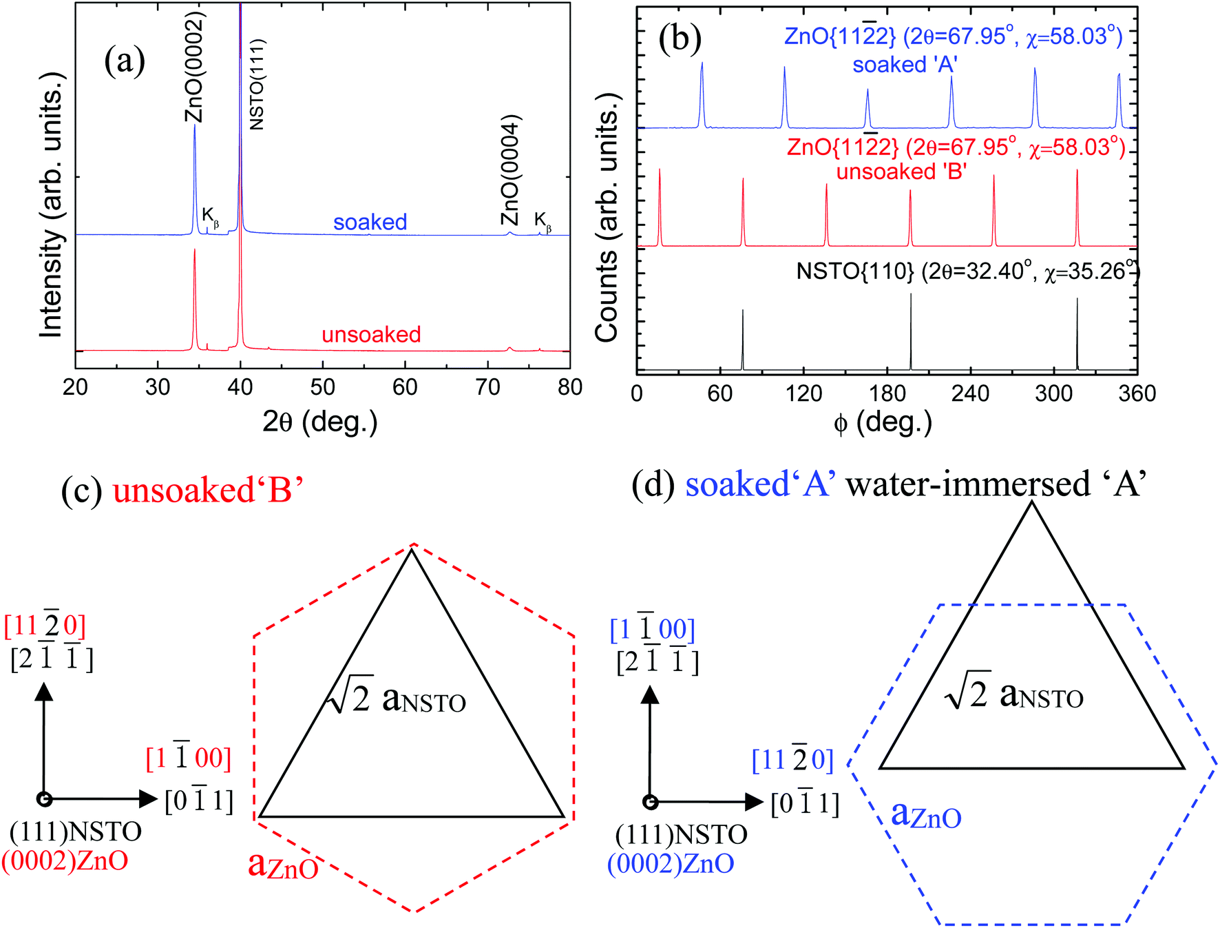 | ||
| Fig. 2 X-ray θ–2θ (a) and Φ (b) scanning patterns of ZnO films grown on unsoaked and deionized water soaked NSTO substrates. The two kinds of in-plane epitaxial relationships between ZnO and NSTO are shown in (c and d). | ||
It is well known that the interface energy (σinterface) plays an important role in the in-plane epitaxial relationship.22 For ZnO/NSTO heterostructure, σinterface = σZnO + σNSTO – γ, where σZnO and σNSTO are the surface energies of ZnO and NSTO, γ is the adhesion energy between ZnO and NSTO. For both in-plane epitaxial relationships, σZnO and σNSTO remain invariable since the surface orientation of ZnO and NSTO does not change, so σinterface depends on γ, which is proportional to the bonding density at the ZnO/NSTO interface. To evaluate the bonding densities at the ZnO/NSTO interfaces, the in-plane atomic arrangement was considered for the case of SrO3- and Ti-terminated surfaces in two in-plane epitaxial relationships. Fig. 3(a, c, e and g) show schematic top views of the ZnO/NSTO interface for SrO3-and Ti-terminated surfaces with the in-plane epitaxial relationships of ‘A’ and ‘B’, respectively. In these figures, only the O and Sr/Ti atoms closest to the interface are shown. In Fig. 3(b, d, f and h), Sr–O/Ti–O bonds and dangling bonds are indicated by solid and open circles, respectively. According to the bonding states in Fig. 3(b, d, f and h), the bonding densities for the in-plane epitaxial relationships of ‘A’ and ‘B’ are 2.7 × 10¹⁴ and 2.3 × 1014 cm−2 on SrO3-terminated substrate, whereas those are 1.3 × 10¹⁴ and 3.6 × 1014 cm−2 on Ti-terminated substrate, respectively. Therefore, σinterface for ‘A’ is higher than that for ‘B’ on SrO3-terminated NSTO, but σinterface for ‘A’ is lower than that for ‘B’ on Ti-terminated STO. Hence, the in-plane epitaxial relationships of ‘B’ and ‘A’ are preferred for ZnO films on SrO3- and Ti-terminated NSTO, respectively. Additionally, the bonding density of ‘B’ on unsoaked SrO3-terminated surface is higher than that of ‘A’ on deionized water soaked Ti-terminated surface, implying that the dangling bond density of ZnO/unsoaked-NSTO is lower than that of ZnO/soaked-NSTO, so we can expect a lower interface state density of ZnO/unsoaked-NSTO than that of ZnO/soaked-NSTO heterojunction.
 | ||
| Fig. 3 Schematic top views (a, c, e and g) and distribution of O atoms bonded to SrO or Ti atoms (b, d, f and h) of the (0001) ZnO/(111)NSTO interface for the in-plane epitaxial relationships of [110]ZnO//[10]NSTO (‘A’) and [100]ZnO//[110]NSTO (‘B’), in which (a–d) are on SrO3-terminated NSTO, while (e–h) are on Ti-terminated NSTO. The O and SrO/Ti atoms closest to the interface are only shown in (a, c, e and g). The crystallographic directions have been indicated for alignment ‘A’ (i) and ‘B’ (j), irrespective of SrO3- or Ti-terminated NSTO. | ||
To analyze the interface state density of the ZnO/NSTO heterojunction, we measured the capacitance–voltage curve of the ZnO/NSTO heterojunction from 1 kHz to 1 MHz, as shown in Fig. 4. A much larger capacitance peak of the ZnO film on deionized water soaked NSTO substrate is observed than that of ZnO on unsoaked substrate at the same frequency of 1 kHz. The interface state densities of both heterojunctions can be achieved from the formula of Nss = Css/q2A, where Nss is the interface state density, Css is the peak capacitance at low frequency, A is the area of top electrode.26 The interface state density of the ZnO/soaked-NSTO heterojunction is calculated to be 2.1 × 10¹³ eV−1 cm−2, which is much larger than that of ZnO/unsoaked-NSTO heterojunction of 2.2 × 10¹² eV−1 cm−2. This is fully consistent with the higher bond density in the ZnO/soaked-NSTO in Fig. 3. There is a significant peak around 0.5 V at 1 kHz, which shifts toward a larger voltage as the frequency increases. These results imply a high density of positively charged interface states at the ZnO/NSTO interface. Therefore, the ZnO/NSTO heterojunction is mainly a donor-type interface state,14 which is consistent with the high concentrations of oxygen vacancies shown in Fig. 5(c). Will these two ZnO films on unsoaked and soaked NSTO exhibit distinct electrical transport property, like the transition from rectification to bipolar resistive switching observed in BaTiO3/ZnO heterojunction?14
 | ||
| Fig. 4 Capacitance–voltage curves of ZnO/unsoaked-NSTO (a) and ZnO/soaked-NSTO (b) heterojunctions. | ||
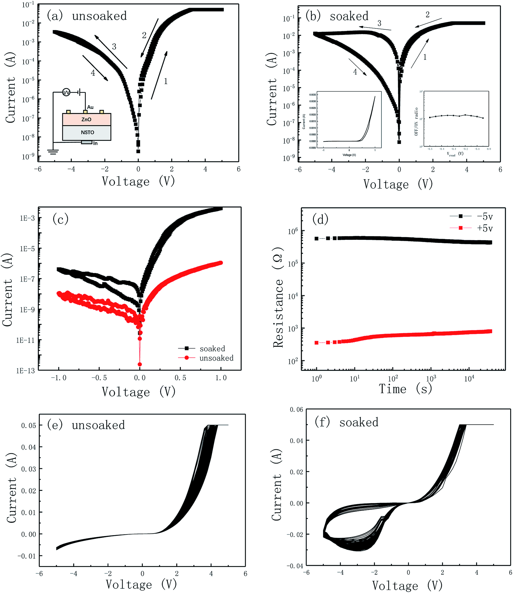 | ||
| Fig. 5 Current–voltage curves of ZnO/unsoaked-NSTO (a) and ZnO/soaked-NSTO (b) heterojunctions, respectively. The inset of (a) shows the device structure. The left and right inset of (b) are the rectification characteristic curve at ± 1 V and ON/OFF ratio readed at −0.1 to −0.5 V. The arrows indicate the sweeping direction of 0 V → +Vmax → 0 V → −Vmax → 0 V. (c) I–V curves of two devices at small voltage. (d) Retention of resistance states in Au/ZnO/soaked-NSTO/In system. I–V curves with 100 cycles of ZnO/unsoaked-NSTO (e) and ZnO/soaked-NSTO (f). | ||
Just as expected, a typical rectification phenomenon is observed in ZnO/unsoaked-NSTO heterojunction with a low interface state density, as shown in Fig. 5(a), the illustration shows the device structure. For the ZnO/soaked-NSTO heterojunction with a high interface state density, a rectification behavior is achieved at a small positive bias, as shown in the figure on the left of Fig. 5(b). While a typical bipolar resistance switching behavior occurs at a sufficiently large voltage, as shown in Fig. 5(b). Obviously, when the bias is sweeping forward, a switching from high resistance state (HRS) to low resistance state (LRS) occurs, which is the SET process. While the bias is sweeping backward, the device is switched back to HRS, which is the RESET process. The right inset of Fig. 5(b) shows a high and stable ON/OFF ratio of 1000 readed at −0.1 to −0.5 V. At a small voltage of Fig. 5(c), both devices exhibit a typical rectification phenomenon of the Schottky junction, and the rectification behavior can be attributed to the variance in the width of the depletion layer. By calculation, the ideal factor and barrier height, are 2.63, 0.86 eV for the unsoaked device, and 2.9 and 0.76 eV for the soaked device, respectively. The rectification ratio is about 100 for the unsoaked device. The reduce of barrier height and increment of current and ideal factor on soaked substrates is consistent with the increase in interface state density and concentration of oxygen vacancies. As the concentration increases of oxygen vacancies, its movement induces bipolar resistance switching characteristics. As shown in Fig. 5(d), after applying the positive (negative) voltage, the low (high) resistance state is obtained after 5 hours, showing excellent stability of the device. Fig. 5 shows the I–V curves with 100 cycles in ZnO/unsoaked-NSTO (e) and ZnO/soaked-NSTO (f) heterojunctions. The good cyclic repeatability is very important for the practical application of the device.
Actually, bipolar RS have been observed in ZnO/(100) NSTO heterojunction without pretreating substrates with dionized water.11 We proposed a model for this behavior, in which the space charge region in ZnO is wide in HRS when the interface state is unoccupied, while the space charge region becomes narrower in LRS due to Fermi pinning when the interface state is completely occupied, and the LRS remains until electrons are detrapped from the interface state. However, the density of interface state in ZnO/(100) NSTO heterojunction is almost two orders of magnitude larger than the value in ZnO/unsoaked-(111) NSTO heterojunction in the present work. This can be understood from the fact that the bonding density at the ZnO/(100) NSTO interface is much lower than that at ZnO/unsoaked-(111) NSTO interface.8 Since the interface state density is close to that in ZnO/(100) NSTO heterojunction, the bipolar RS appear in the ZnO/soaked-(111) NSTO heterojunction too.
Two decay models were adopted to understand the retention behavior, the power function decay mechanism of Fig. 6(a and b) can be ruled out because our data does not follow the power function decay. The exponential decay of Fig. 6(c and d) is an evidence of the movement of nano-ions observed in MoOx/MoS2 devices, which corresponds to the migration of oxygen vacancies.27 Compared with the unsoaked device, the interface state density and the concentration of oxygen vacancies are increased in the soaked device, resulting in a rectification from rectification to bipolar resistive transition.
 | ||
| Fig. 6 Experimental data and fitting curve of device under different resistance in ZnO/soaked-NSTO. The red curve of (a and b) are fits to a power law for the decay of resistance state. The red curves of (c and d) are fits to an exponential relaxation equation. | ||
In the ZnO/unsoaked-NSTO heterojunction, the oxygen vacancies are too low to affect the electrical transport properties, and only the rectification curve is observed in Fig. 5(a). A schematic diagram of the substrate pretreatment induced RS process is shown in Fig. 7, the concentration of oxygen vacancies in the ZnO/soaked-NSTO heterojunction density increase, which will participate in the electrical transport process. The oxygen vacancies with positive charge will drift toward (away from) the ZnO/soaked-NSTO Schottky junction interface under positive (negative) voltage bias. In this way, the accumulation (segregation) of oxygen vacancies at the ZnO/soaked-NSTO interface will trigger the LRS (HRS) state, which is the behavior observed in Fig. 5(b). This has also found in the Au/BTO and ZnO/(100) NSTO heterojunction.8,15
 | ||
| Fig. 7 The schematic accumulation (segregation) of oxygen vacancies at the Au/ZnO/soaked-NSTO (a and b) heterojunctions. Black arrow indicates drift direction of oxygen vacancies, the orange hollow sphere represents the oxygen vacancies. | ||
4. Conclusions
In conclusion, the NSTO substrate pretreatment has significant influence on growth behavior and electrical properties of ZnO films. The out-of-plane orientation of ZnO films were both along the c-axis, while the in-plane orientation is strongly dependent on substrate pretreatment. Furthermore, a transition from rectification to bipolar resistance switching was found in ZnO films on unsoaked and soaked NSTO substrates, which is consistent with the increase of oxygen vacancies concentration.Conflicts of interest
There are no conflicts to declare.References
- Z. L. Wang and J. H. Song, Science, 2006, 312, 242–246 CrossRef CAS PubMed.
- L. P. Zhu, Y. Zhang and P. Lin, ACS Nano, 2018, 12, 1811–1820 CrossRef CAS PubMed.
- L. P. Zhu, L. F. Wang and F. Xue, Adv. Sci., 2016, 4, 1600185 CrossRef PubMed.
- J. J. Lee, F. T. Schmitt and R. G. Moore, Nature, 2013, 515, 245–248 CrossRef.
- J. H. Kang, L. Xie and Y. Wang, Nano Lett., 2018, 18, 6347–6352 CrossRef CAS.
- W. S. Choi, S. A. Lee and J. H. You, Nat. Commun., 2015, 6, 7424 CrossRef CAS PubMed.
- A. Infortuna, P. Muralt and M. Cantoni, J. Appl. Phys., 2006, 100, 104110 CrossRef.
- C. H. Jia, Y. H. Chen and X. L. Liu, J. Appl. Phys., 2013, 8, 23 Search PubMed.
- A. Bera, H. Y. Peng and J. Lourembam, Adv. Funct. Mater., 2013, 23, 4977–4984 CrossRef CAS.
- Y. L. Wu, L. W. Zhang and G. L. Xie, Appl. Phys. Lett., 2008, 92, 012115 CrossRef.
- C. H. Jia, X. W. Sun and G. Q. Li, Appl. Phys. Lett., 2014, 104, 043501 CrossRef.
- M. Han, Y. Ren and J. C. Li, Vacuum, 2017, 142, 66–71 CrossRef CAS.
- Y. L. Fang, J. C. Li and Y. H. Chen, Phys. B, 2017, 521, 69–72 CrossRef CAS.
- C. H. Jia, X. Q. Yin and G. Yang, Appl. Phys. Lett., 2017, 111, 113506 CrossRef.
- G. Yang, C. H. Jia and Y. H. Chen, J. Appl. Phys., 2014, 115, 204515 CrossRef.
- H. L. Ma, W. Wang and H. Y. Xu, ACS Appl. Mater. Interfaces, 2018, 10, 21755–21763 CrossRef CAS PubMed.
- C. R. Cho, S. I. Kwun and T. W. Noh, Jpn. J. Appl. Phys., 1997, 36, 2196–2199 CrossRef CAS.
- B. C. Russell and M. R. Castell, Phys. Rev. B: Condens. Matter Mater. Phys., 2007, 75, 155433 CrossRef.
- B. C. Russell and M. R. Castell, J. Phys. Chem. C, 2008, 112, 6538–6545 CrossRef CAS.
- A. GÖMann, K. GÖMann and M. Frerichs, Appl. Surf. Sci., 2005, 252, 196–199 CrossRef.
- S. Sekiguchi, M. Fujimoto and M. Nomura, Solid State Ionics, 1998, 108, 73–79 CrossRef CAS.
- K. Hirama, Y. Taniyasu and M. Kasu, Appl. Phys. Lett., 2011, 98, 162112 CrossRef.
- J. Chang, Y. S. Park and S. K. Kim, Appl. Phys. Lett., 2008, 92, 152910 CrossRef.
- A. H. Johnstone, J. Chem. Technol. Biotechnol., 2007, 327–328 CrossRef.
- C. H. Jia, Y. H. Chen and B. Zhang, Appl. Surf. Sci., 2012, 258, 2927–2930 CrossRef CAS.
- E. H. Nicollian and A. Goetzberger, Bell System Technical Journal, 1967, 46, 1055–1133 CrossRef CAS.
- A. A. Bessonov, M. N. Kirikova and D. I. Petukhov, Nat. Mater., 2014, 14, 199 CrossRef.
| This journal is © The Royal Society of Chemistry 2019 |