
 Open Access Article
 This Open Access Article is licensed under a Creative Commons Attribution-Non Commercial 3.0 Unported Licence
Resistive switching behavior in α-In2Se3 nanoflakes modulated by ferroelectric polarization and interface defects†
Pengfei
Hou‡
 *ab,
Siwei
Xing‡
ab,
Xin
Liu‡
ab,
Cheng
Chen
ab,
Xiangli
Zhong
a,
Jinbin
Wang
*a and
Xiaoping
Ouyang
*a
*ab,
Siwei
Xing‡
ab,
Xin
Liu‡
ab,
Cheng
Chen
ab,
Xiangli
Zhong
a,
Jinbin
Wang
*a and
Xiaoping
Ouyang
*a
aKey Laboratory of Low-dimensional Materials and Application Technology, School of Materials Science and Engineering, Xiangtan University, Xiangtan 411105, Hunan, China. E-mail: houpf@xtu.edu.cn; jbwang@xtu.edu.cn; oyxp2003@aliyun.com
bScience and Technology on Reliability Physics and Application Technology of Electronic Component Laboratory, Guangzhou 510610, Guangdong, China
First published on 26th September 2019
Abstract
Resistive switching devices based on ferroelectric two-dimensional (2D) van der Waals (vdW) nanomaterials may display simple structures, high density, high speed, and low power consumption, and can be used in flexible electronics and highly integrated devices. However, only a few studies about the in-plane (IP) resistive switching behavior of ferroelectric 2D vdW nanomaterials have been reported because it is very hard to achieve asymmetric barriers only by tuning the IP polarization directions when the electrodes of the planar device are all of the same type. In the current work, we developed a planar device based on an α-In2Se3 nanoflake, in which the IP/OOP (out-of-plane) polarization, free carriers and oxygen vacancies in SiO2 contribute to the resistive switching behavior of the device. This behavior of the device was shown to be affected by exposure to light, and the photoelectric performance was also investigated when the device was in the OFF state. The demonstration of this planar resistive switching device may promote the further development of resistive devices based on 2D vdW nanomaterials, and provide great inspiration for the development of new kinds of transistors.
1. Introduction
Two-dimensional (2D) van der Waals (vdW) nanomaterials have attracted widespread attention from engineers and scientists due to their unique physical and chemical properties, including their novel electronic, magnetic, thermal, and optical properties.1–5 An increasing number of new kinds of 2D vdW nanomaterials have been explored, benefiting from the development of new preparation technologies, and they can be used as insulators, semiconductors, semimetals, metals and superconductors for intelligent structures, electronics and optoelectronics, and energy storage and conversion.1–4 Ferroelectric 2D vdW nanomaterials are particularly special because of their spontaneous in-plane (IP) or out-of-plane (OOP) polarizations, and have been investigated for application in memories, capacitors, actuators, transistors and sensors.6–10 Resistive switching devices based on 2D vdW nanomaterials may show simple structures, high density, high speed, and low power consumption, and they furthermore can be used in flexible electronics and highly integrated devices.11 For ferroelectric resistive switching devices, ferroelectric polarizations are always used to construct different asymmetric interface barriers to realize resistive switching behavior.12 However, only a few studies about the IP resistive switching behavior of ferroelectric 2D vdW nanomaterials have been reported because it is very hard to achieve different asymmetric barriers for different resistance states only by tuning IP polarization directions when the electrodes of the planar device are all of the same type.7 α-In2Se3 is a 2D vdW ferroelectric material with a bandgap of only about 1.3 eV, and is particularly special because of its intrinsically intercorrelated IP and OOP polarizations.10,13,14 This feature indicates that α-In2Se3 is a suitable material for planar ferroelectric resistive switching devices, because OOP polarization can assist the IP polarization to promote the formation of different asymmetric barriers for different resistance states.In the current work, we proposed a planar resistive switching device based on α-In2Se3 nanoflakes, and investigated their resistive switching mechanism. Furthermore, the effect of light on the resistive switching behavior was also explored. Although the switch ratio of the planar resistive switching device needs to be improved, we expect this device to have great development and application potential because of its simple structure, high density, high speed, low power consumption and possible application in flexible devices and highly integrated devices.
2. Preparation and mechanism
Fig. 1(a) shows a schematic of the device used in our experiment, specifically the planar resistive switching device based on α-In2Se3 nanoflakes. The figure also shows the circuit used to carry out the resistive switching measurements. A bulk α-In2Se3 crystal, purchased from a 2D semiconductor company, was subjected to mechanical exfoliation to produce the α-In2Se3 nanoflakes. Pt electrodes were then fabricated by carrying out dc sputtering through a shadow mask of about 50 μm at room temperature. Fig. 1(b) shows an optical micrograph of the planar device on a 300 nm-thick SiO2-coated Si substrate annealed for 2 minutes at 600 °C in an Ar atmosphere to produce oxygen defects. The energy band structure of the planar resistive switching device is shown in Fig. 1(c). Due to the α-In2Se3 nanoflakes being a ferroelectric semiconductor material that simultaneously displays IP and OOP polarizations, the OOP polarization switches to the opposite direction upon switching the direction of the IP polarization.6–10,15 The switching of OOP polarization may promote the redistribution of free carriers in α-In2Se3. Considering the IP and OOP polarizations, redistribution of free carriers and defects in SiO2, we proposed a mechanism that would realize resistive switching behavior, as shown in Fig. 1(d). According to this mechanism, pointing the OOP polarization up (see Fig. 1(d)) would pull the electrons away from the interface of α-In2Se3 and the SiO2-coated Si substrate, and lead to an ON state or low-resistance state for the planar resistive switching device. Switching the direction of the OOP polarization would pull the electrons toward this interface – and result in some or many of such electrons becoming captured by any oxygen defects located near the surface of the SiO2-coated Si substrate, leading to a decrease in the conductivity of the device and hence resulting in an OFF state or high-resistance state. In order to verify this mechanism, we measured the characteristics of the α-In2Se3 flakes and the electrical properties of the planar device.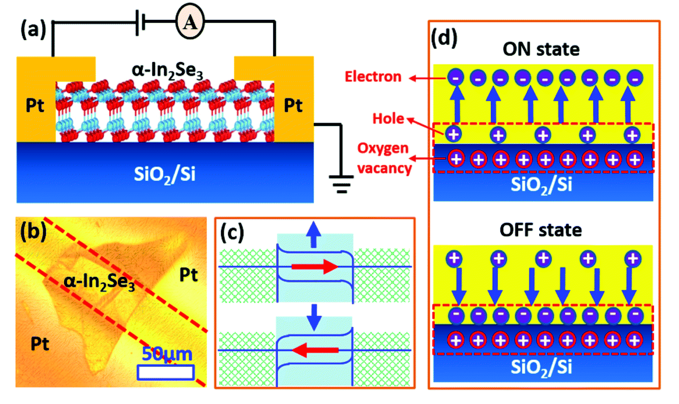 | ||
| Fig. 1 (a and b) Schematic and optical micrograph of the planar device based on α-In2Se3 nanoflakes. (c) The polarization-direction-dependent band alignment. (d) Schematic of the possible polarization-induced motion of free carriers. | ||
3. Results and discussion
Raman spectral measurements of α-In2Se3 and Pt-coated α-In2Se3 were taken using a 532 nm-wavelength excitation laser and a Renishaw inVia Raman microscope, and the results are shown in Fig. 2(a). For both α-In2Se3 and Pt-coated α-In2Se3, peaks were observed at ∼88, 103, 182, 193 and 204 cm−1 and were attributed to the E, A(LO + TO), A(LO), A(TO) and A(LO) (LO = longitudinal optical, TO = transverse optical) phonon modes of α-In2Se3. The thickness of the Pt electrode was only about 8–10 nm, so the Raman spectra of α-In2Se3 and Pt-coated α-In2Se3 were essentially identical. The presence of the A(LO) and A(TO) modes at 182 and 193 cm−1 was caused by LO–TO splitting and indicated a lack of inversion symmetry in the R3m structure.13–15 We also measured the ferroelectricity of an α-In2Se3 nanoflake by performing atom force microscopy (AFM, Asylum Research MFP-3D Infinity). The local piezoelectric loops of the α-In2Se3 flake were measured by varying the bias on the sample with a conductive AFM tip and the heavily doped Si substrate. As shown in Fig. 2(b), a butterfly-shaped voltage-dependent amplitude loop was observed, along with a sharp change in phase up to 180°, typical for ferroelectrics. Amplitude and phase images of part of an α-In2Se3 nanoflake in the planar device were acquired using a piezoelectric atomic force microscope (PFM) mode of the AFM, as shown in Fig. 2(c)–(f). The thickness of the nanoflake was about 30 nm, and spontaneously formed ferroelectric domains were directly visualized in the OOP/IP PFM phase images. 180° PFM phase contrast contributions were observed, indicating the antiparallel ordering of electric dipoles in the OOP/IP directions between the adjacent ferroelectric domains. All of the results shown in Fig. 2 provide evidence for the good ferroelectricity of the α-In2Se3 nanoflakes.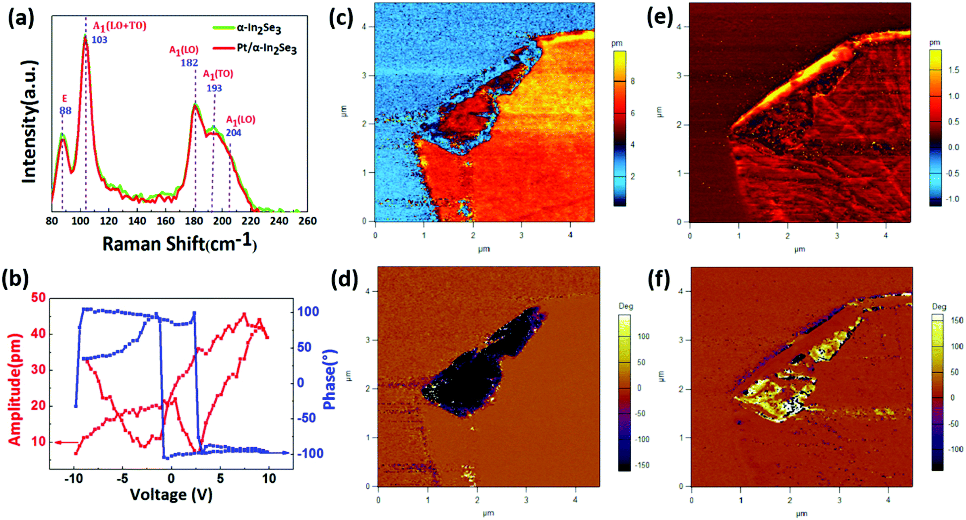 | ||
| Fig. 2 (a) Raman spectra of an α-In2Se3 nanoflake and Pt-coated α-In2Se3 nanoflake each subjected to 532 nm-wavelength laser excitation. (b) Amplitude and phase loops of an α-In2Se3 nanoflake measured using PFM. (c and d) Amplitude and phase images for the OOP direction. (e and f) Amplitude and phase images for the IP direction. | ||
In order to investigate the resistive switching behavior of the planar device, I–V curves were acquired using an Agilent B1500A semiconductor device analyzer. Due to the band gap of α-In2Se3 being only about 1.3 eV, we suspected that the resistive switching behavior of the device may be affected by light. A solar simulator was used to control the light conditions during the measurements. I–V characteristics of the planar device exposed to light are shown in Fig. 3(a), and were used to evaluate the resistance characteristics. The corresponding current was measured with voltage sweeps of 0 V → negative/positive voltage, with the arrows in the figure showing the change of the current. In the voltage sweeps, the state with high current was the ON state, while the state with low current was the OFF state. First, a voltage sweep of 0 V → 7 V was applied to the device, resulting in an ON state. The first sweep was denoted as the READ1/SET process. Then another voltage sweep of 0 V → 7 V was applied to the device to read the state; here, the state did not change, and the process was denoted as the READ2 process. However, the state switched from ON to OFF when a voltage sweep of 0 V → −10 V was applied to the device, and this process was denoted as the READ3/RESET process. When another voltage sweep of 0 V → −10 V was applied to the device to read the state, the state did not change, and the process was denoted as the READ4 process. The same operation was repeated in the dark, and the results are shown in Fig. 3(b). A clearly sudden change occurred at 4 V in the READ1/SET process, and this voltage was an obvious SET voltage for the resistive switching behavior.16 On the other hand, a different sudden change was also observed at −8.5 V in the READ3/RESET process, and this voltage was an obvious RESET voltage in the resistive switching behavior.16 The SET/RESET voltages were not obvious when the device was exposed to light. Such SET and RESET voltages are typical characteristic parameters, and these parameters can be used to evaluate the performance of resistive switching memory. The acquired I–V curves showed that the resistive switching behavior of the α-In2Se3-based planar resistive switching device can be affected by the light/dark conditions. In addition, we noted another big difference between the I–V curves: that the current of the OFF state in the dark was much lower than the current for the device exposed to light. As illustrated in Fig. 1(d), the resistive switching behavior of the device was based on the collective effect of interface defects of SiO2, free carriers and IP/OOP polarizations in α-In2Se3. The difference between the low-current states under light and dark conditions appeared to provide evidence for our proposed resistive switching mechanism, because the light may have promoted the migration of electrons trapped by the defects of SiO2 when the polarization of α-In2Se3 was pointing down, resulting in I–V curves showing high current when the device was in the OFF state. The main mechanism is shown in the inset of Fig. 3. In order to prove our mechanism, a device with few oxygen vacancies was prepared, and its I–V curves are shown in Fig. S1.† No obvious resistive switching was achieved. For easy comparison, we plotted the I–V curves resulting from dark and light conditions in one panel as shown in Fig. S2.†
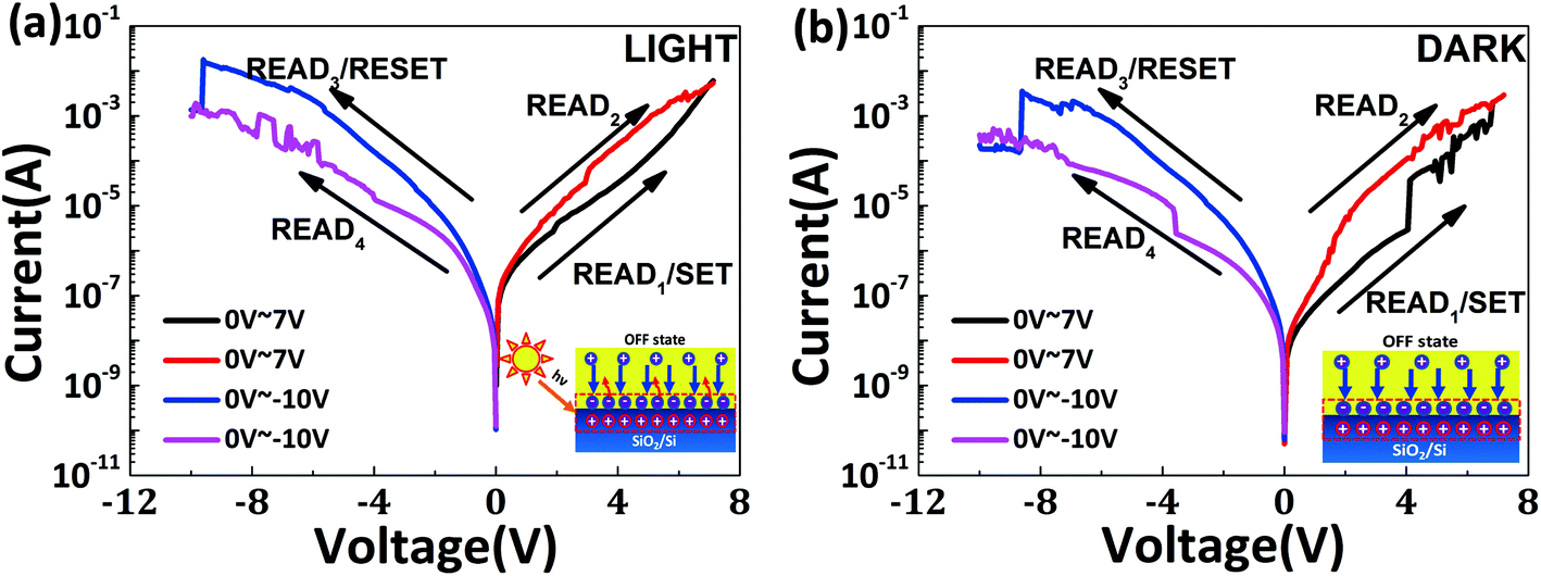 | ||
| Fig. 3 Currents of the Pt/α-In2Se3/Pt device at various applied voltages (a) with visible light illumination and (b) without visible light illumination. The inset figures show the photoelectric effect mechanism for the OFF states. | ||
Considering that the difference between the I–V curves resulting from the dark and from illumination may have been caused by the photoconduction effect when the device was in the OFF state, the transient current waveform in response to a series of cycles with alternating ON and OFF states of the solar simulator source was acquired, as shown in Fig. 4(a). The input optical power density at the measurement position was approximately 7.2 mW cm−2. The planar resistive switching device exhibited a repeatable and reasonably stable response to incident light. Usually, the rise time is defined as the amount of time it takes for the photocurrent to increase from 10% to 90% of its maximum value, and the fall time is defined as the amount of time it takes for the photocurrent to decrease from 90% to 10% of its maximum value. However, the current in our device was higher than those of reported works – and, in our experiments, the temperature change resulting from the Joule heat produced during the measurement and the light may have affected the current a lot. For our device, the rise time was defined as the amount of time it took for the current to increase from 0.1 to 6.3 μA (which it did so suddenly), while the fall time was defined as the amount of time it took for the current to decrease from 8.9 to 3.7 μA (which it also did so suddenly), as shown in Fig. 4(b). The response time was calculated by averaging the duration of values between light-ON and light-OFF. For our device, the rise and fall times were specifically measured to be 47 and 87 ms, respectively. In all, the response performance confirmed our proposed mechanism. The retention characteristics of the planar resistive switching device in the dark is shown in Fig. S3;† the resistance states of the device were observed to be stable for a relatively long time.
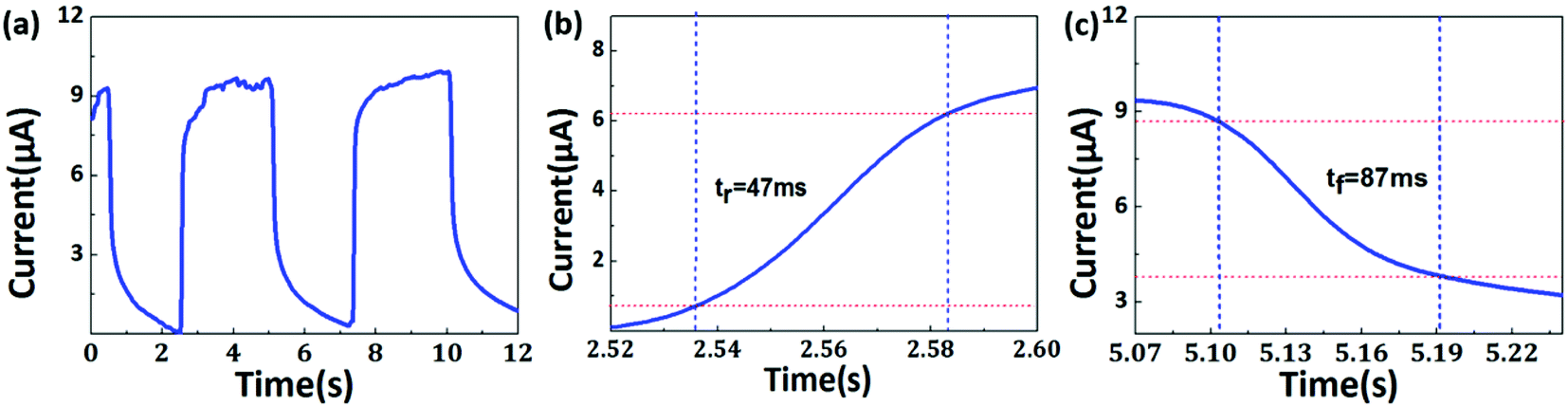 | ||
| Fig. 4 (a) I−t curve of the planar In2Se3 device with and without visible light illumination. (b and c) Magnified views of the curve showing examples of (b) the rise and (c) fall of the current with time. | ||
Resistive switching memory has been investigated for quite a while, and many resistive switching mechanisms have been proposed, including migrations of Ag/Cu ions, migration of defects, interface effects and so on.16–18 The most important part of these devices is that producing the two different resistance states. In our device, the IP polarization was indicated to contribute to the interface barrier to restrain the high conductivity, while the OOP polarization and defects in SiO2 promoted the asymmetrical distribution of interface electrons when the polarization was switched. In fact, our α-In2Se3-based planar resistive switching device acted much more like a transistor. However, no gate voltage was needed in our device, and just the application of a planar electric field was able to write and read the memory states.19 The low value of the switch ratio of the device may not affect its application. High switch ratios are always needed to restrain the misreading in resistive switching memories made of cross-bar array structures.20,21 But our device was designed with a planar structure, and realized a three-dimensional stacking structure without a cross-bar array structure; hence misreading was easily restrained. Furthermore, the 2D vdW nanomaterial-based resistive switching memory may have great applications in flexible electronics, which are important in artificial intelligence and wearable devices, especially devices designed to be sensitive to light.1–4,20
4. Summary
In summary, we have designed a planar resistive switching device based on an α-In2Se3 nanoflake, and the resistive switching mechanism was proven experimentally. The resistive switching behavior of the device was affected by the light condition, and the photoelectric performance for the device in the OFF state was also investigated. This demonstration of a planar resistive switching device may promote the further development of resistive devices based on 2D vdW nanomaterials, and provide great inspiration for developing new kinds of transistors. The device may find promising applications involving artificial intelligence, wearable devices and photosensitive devices.Conflicts of interest
There are no conflicts to declare.Acknowledgements
This work was supported by the Natural Science Foundation of Hunan Province, China (Grant No. 2019JJ50582), the Opening Project of Science and Technology on Reliability Physics and Application Technology of Electronic Component Laboratory, China (No. ZHD201803), the Open Project Program of Key Laboratory of Low-Dimensional Materials & Application Technology (Xiangtan University), Ministry of Education, China (No. KF20180204), and the National Natural Science Foundation of China (No. 51872251, 61574121).References
- A. C. Ferrari, F. B. V. Fal'ko, K. S. Novoselov, S. Roche, P. Bøggild, S. Borini, F. H. L. Koppens, V. Palermo, N. Pugno, J. A. Garrido, R. Sordan, A. Bianco, L. Ballerini, M. Prato, E. Lidorikis, J. Kivioja, C. Marinelli, T. Ryhänen, A. Morpurgo, J. N. Coleman, V. Nicolosi, L. Colombo, A. Fert, M. G. Hernandez, A. Bachtold, G. F. Schneider, F. Guine, C. Dekker, M. Barbone, Z. Sun, C. Galiotis, A. N. Grigorenko, G. Konstantatos, A. Kis, M. Katsnelson, L. Vandersypen, A. Loiseau, V. Morandi, D. Neumaier, E. Treossi, V. Pellegrini, M. Polini, A. Tredicucci, G. M. Williams, B. H. Hong, J. H. Ahn, J. M. Kim, H. Zirath, B. J. Wees, H. Zant, L. Occhipinti, A. D. Matteo, I. A. Kinloch, T. Seyller, E. Quesnel, X. Feng, K. Teo, N. Rupesinghe, P. Hakonen, S. R. T. Neil, Q. Tannock, T. Löfwander and J. Kinaret, Nanoscale, 2015, 7(11), 4598–4810 RSC.
- S. Z. Butler, S. M. Hollen, L. Cao, Y. Cui, J. A. Gupta, H. R. Gutierrez, T. F. Heinz, S. S. Hong, J. Huang, Z. A. F. Ismach, E. J. Halperin, M. Kuno, V. V. Plashnitsa, R. D. Robinson, R. S. Ruoff, S. Salahuddin, J. Shan, L. Shi, O. M. G. Spencer, M. Terrones, W. Windl and J. E. Goldberger, ACS Nano, 2013, 7(4), 2898–2926 CrossRef CAS.
- G. R. Bhimanapati, Z. Lin, V. Meunier, Y. Jung, J. Cha, S. Das, D. Xiao, Y. Son, M. S. Strano, V. R. Cooper, L. Liang, S. G. Louie, E. Ringe, W. Zhou, S. S. Kim, R. R. Naik, B. G. Sumpter, H. Terrones, F. Xia, Y. Wang, J. Zhu, D. Akinwande, N. Alem, A. Schuller, R. E. Schaak, M. Terrones and J. A. Robinson, ACS Nano, 2015, 9(12), 11509–11539 CrossRef CAS.
- M. Zeng, Y. Xiao, J. Liu, Y. Kena and F. Lei, Chem. Rev., 2018, 118(13), 6236–6296, DOI:10.1021/acs.chemrev.7b00633.
- K. S. Burch, D. Mandrus and J. G. Park, Nature, 2018, 563(7729), 47 CrossRef CAS.
- J. Xiao, H. Zhu, Y. Wang, W. Feng, Y. Hu, A. Dasgupta, Y. Han, Y. Wang, D. A. Muller, L. W. Martin, P. Hu and X. Zhang, Phys. Rev. Lett., 2018, 120, 227601 CrossRef CAS.
- F. Xue, W. Hu, K. -C. Lee, L. -S. Lu, J. Zhang, H. -L. Tang, A. Han, W. -T. Hsu, S. Tu, W. -H. Chang, C. -H. Lien, J. -H. He, Z. Zhang, L. -J. Li and X. Zhang, Adv. Funct. Mater., 2018, 28, 1803738 CrossRef.
- M. Si, P. Y. Liao, G. Qiu, Y. Duan and P. D. Ye, ACS Nano, 2018, 12(7), 6700–6705 CrossRef CAS.
- F. Xue, X. He, J. R. D. Retamal, A. Han, J. Zhang, Z. Liu, J. -K. Huang, W. Hu, V. Tung, J. -H. He, L. -J. Li and X. Zhang, Adv. Mater., 2019, 31, 1901300 CrossRef.
- P. Hou, Y. Lv, X. Zhong and J. Wang, ACS Appl. Nano Mater., 2019, 2(7), 4443–4450 CrossRef CAS.
- Y. Li, X. Y. Sun, C. Y. Xu, J. Cao, Z. Y. Sun and L. Zhen, Nanoscale, 2018, 10(48), 23080–23086 RSC.
- P. Hou, J. Wang and X. Zhong, Sci. Rep., 2017, 7(1), 4525 CrossRef.
- Y. Zhou, D. Wu, Y. Zhu, Y. Cho, Q. He, X. Yang, K. Herrera, Z. Chu, Y. Han, M. C. Downer, H. Peng and K. Lai, Nano Lett., 2017, 17(9), 5508–5513 CrossRef CAS PubMed.
- F. Xue, J. Zhang, W. Hu, W. T. Hsu, A. Han, Si. F. Leung, J. K. Huang, Y. Wan, S. Liu, J. Zhang, J. H. He, W. H. Chang, Z. L. Wang, X. Zhang and L. J. Li, ACS Nano, 2018, 12(5), 4976–4983 CrossRef CAS.
- C. Cui, W. J. Hu, X. Yan, C. Addiego, W. Gao, Y. Wang, Z. Wang, L. Li, Y. Cheng, P. Li, X. Zhang, H. N. Alshareef, T. Wu, W. Zhu, X. Pan and L. J. Li, Nano Lett., 2018, 18(2), 1253–1258 CrossRef CAS.
- P. Hou, J. Wang, X. Zhong and Y. Wu, RSC Adv., 2016, 6(59), 54113–54118 RSC.
- X. Zhao, Z. Fan, H. Xu, Z. Wang, J. Xu, J. Ma and Y. Liu, J. Mater. Chem. C, 2018, 6(27), 7195–7200 RSC.
- Y. T. Tseng, I. C. Chen, T. C. Chang, J. C. Huang, C. C. Shih, H. X. Zheng, W. C. Chen, M. H. Wang, W. C. Huang, M. C. Chen, X. H. Ma, Y. Hao and S. M. Sze, Appl. Phys. Lett., 2018, 113(5), 053501 CrossRef.
- M. Si, P. Y. Liao, G. Qiu, Y. Duan and P. D. Ye, ACS Nano, 2018, 12(7), 6700–6705 CrossRef CAS.
- D. Ielmini, Semicond. Sci. Technol., 2016, 31(6), 063002 CrossRef.
- U. Chand, K. C. Huang, C. Y. Huang, C. H. Ho, C. H. Lin and T. Y. Tseng, J. Appl. Phys., 2015, 117(18), 184105 CrossRef.
Footnotes |
| † Electronic supplementary information (ESI) available. See DOI: 10.1039/c9ra06566k |
| ‡ These are the coauthors in this work. |
| This journal is © The Royal Society of Chemistry 2019 |