DOI:
10.1039/C9RA06470B
(Paper)
RSC Adv., 2019,
9, 31233-31240
Improved uniaxial dielectric properties in aligned diisopropylammonium bromide (DIPAB) doped poly(vinylidene difluoride) (PVDF) nanofibers†
Received
19th August 2019
, Accepted 25th September 2019
First published on 2nd October 2019
Abstract
Diisopropylammonium bromide (DIPAB) doped poly(vinylidene difluoride) (PVDF) nanofibers (5, 10 and 24 wt% DIPAB doping) with improved and tunable dielectric properties were synthesised via electrospinning. DIPAB nanoparticles were grown in situ during the nanofiber formation. X-Ray diffraction (XRD) patterns and Fourier transform infrared spectroscopy (FTIR) proved that electrospinning of DIPAB doped PVDF solutions led to the formation of a highly electro-active β-phase in the nanofibers. Electrospinning in the presence of DIPAB inside PVDF led to very well aligned nanofibers with preferred (001) orientation that further enhanced the effective dipole moments in the nanofiber structures. The dielectric properties of the composite nanofibers were significantly enhanced due to the improved orientation, ionic and interfacial polarisation upon the applied electrospinning process, ionic nature of DIPAB and the interface between the PVDF nanofibers and equally dispersed DIPAB nanoparticles inside them, respectively. The relative dielectric constant of the PVDF nanofibers was improved from 8.5 to 102.5 when nanofibers were doped with 5% of DIPAB. Incorporating DIPAB in PVDF nanofibers has been shown to be an effective way to improve the structural and dielectric properties of PVDF.
Introduction
Ferroelectric materials are used in many electronic applications and have been studied for over a century for their multifunctional electro-active properties.1 They show spontaneous electric polarisation that can be controlled by an external electric field.2–4 Their temperature dependent and electromechanical properties can be used in pyroelectric5 and piezoelectric6 applications. In recent years, many researchers have started to study organic and molecular ferroelectric materials that became interesting because of their ability to be processed in solutions,7 as well as their stability and ease of use.8
Poly(vinylidene difluoride) (PVDF) has been a material of interest because it shows distinctive piezoelectric, pyroelectric and ferroelectric properties.9,10 It is a semicrystalline polymer that is flexible, lightweight, inexpensive and has a high electrical breakdown strength.11 PVDF belongs to the ‘order–disorder’ ferroelectric class in which the phase transition can take place from randomly oriented dipoles (paraelectric phase) to ordered dipoles (ferroelectric phase). PVDF has a crystallinity of around 50% and can be found in five different polymorphs. The monoclinic α-phase of PVDF is the most commonly occurring polymorph with TGTĞ {Trans–Gauche(+)–Trans–Gauche(−)} chain conformation. The β-phase shows piezoelectricity with an all-trans (TTTT) conformation forming an orthorhombic structure with all the fluorine atoms located on the same side in the polymer crystal structure.9 The other polymorphs include γ (orthorhombic; TTTGTTTĞ conformation), δ and ε, which are polar and anti-polar equivalents to α-phase and γ-phase, respectively.
PVDF has a long range of ordered dipole interactions, a strong ferroelectric phase and a Curie temperature, Tc, higher than its melting temperature, Tm.12 These properties can be used in a wide range of applications including sensors,13 actuators,14 capacitors15 and non-volatile ferroelectric memories.16 The most common α-phase can also be converted easily into β-phase by electrical poling and mechanical drawing.17–19 Despite PVDF's potential as an alternative to the inorganic ferroelectric crystals, it suffers from low dielectric constant (∼8.5 for bulk PVDF) resulting in a low electrical energy density that can be stored within the material.20 This can be overcome by incorporating materials with high dielectric permittivity such as BaTiO3, BaxSr1−xTiO3, Pb(Zr,Ti)O3.21,22 Although these materials have advantages, they are still heavy metals with a high processing temperature.23
Diisopropylammonium bromide (DIPAB) is a molecular, organic and ferroelectric crystal having a room temperature polar point group and a high melting temperature. It exists in two different polymorphs, i.e. 1-F and 1-P.24 The 1-F (ferroelectric phase) belongs to the monoclinic crystal system, while the 1-P (paraelectric phase) belongs to the rhombohedral crystal system at room temperature. The 1-P phase can be easily converted into 1-F phase by heating DIPAB to 428 K. A spontaneous polarisation of 23 μC cm−2 (comparable to that of BaTiO3), a high Tc of 426 K, along with a room temperature dielectric constant of 85 and small loss tangent of 0.44% at the frequency of 400 Hz was reported for pure DIPAB crystals.23,25–27 Hence, DIPAB exhibits a good ferroelectric and piezoelectric response along with well-defined ferroelectric domains and can act as a molecular alternative to perovskite ferroelectrics.
Very few PVDF–DIPAB nanocomposites have been reported in the literature and they were all in the form thin films.9,28 These publications have demonstrated the nanocomposites' potential portraying an enhanced dielectric strength and a good chemical stability in harsh environments. Electrospinning of the PVDF at low temperatures along with fast solvent evaporation result to β-phase formation and it also influences the crystallinity of the nanofibers. Baji et al. showed that electrospinning is said to enhance ferroelectric and piezoelectric phase of PVDF because of uniaxial stretching taking place at high electric potentials.29 The diameter, surface tension and mechanical strength of the fibers are impacted by the electrospinning parameters and type of solvent used. So far, DIPAB–PVDF composites as nanofibers have not been reported.
We studied the properties of uniaxially aligned DIPAB doped PVDF nanofibers formed using rotating drum electrospinning. DIPAB was used along with the PVDF due to its high dielectric constant value and affinity to form in situ nanocrystals with high surface area. The high β-phase PVDF nanofibers with varying loading content of DIPAB have been synthesised and studies with respect to the dielectric properties of the formed structures have been investigated. We found out that there was an improvement in the relative dielectric constant of the DIPAB doped PVDF nanofibers by more than 12 times in comparison to the regular bulk PVDF and this value is higher than the reported value of DIPAB–PVDF films reported earlier in the literature.9,28
Experimental
Materials
All chemicals that were used in the reaction were of analytical grade. The poly(vinylidene difluoride) (HSV 900) in powder form was purchased from MTI chemicals, USA. N,N-dimethylformamide (DMF), diisopropylamine and hydrobromic acid (HBr) were purchased from Sigma Aldrich.
Synthetic procedures
Synthesis of diisopropylammonium bromide.
Diisopropylammonium bromide (DIPAB) crystals were obtained by the slow evaporation of the equimolar solution of diisopropylamine and hydrobromic acid in methanol. The obtained DIPAB crystals were collected and finely ground using mortar and pestle, and stored under inert gas atmosphere.
Preparation of DIPAB doped PVDF solutions for electrospinning.
A 9.8 wt% homogenous solution of PVDF powder in DMF was obtained by heating the mixture at 105 °C for 1.5 hours. Different amounts of DIPAB were then added to the solution. The mixtures were left to stir at room temperature overnight to ensure complete dissolution of DIPAB. The overnight stirring also leads to the removal of air bubbles in the solution.
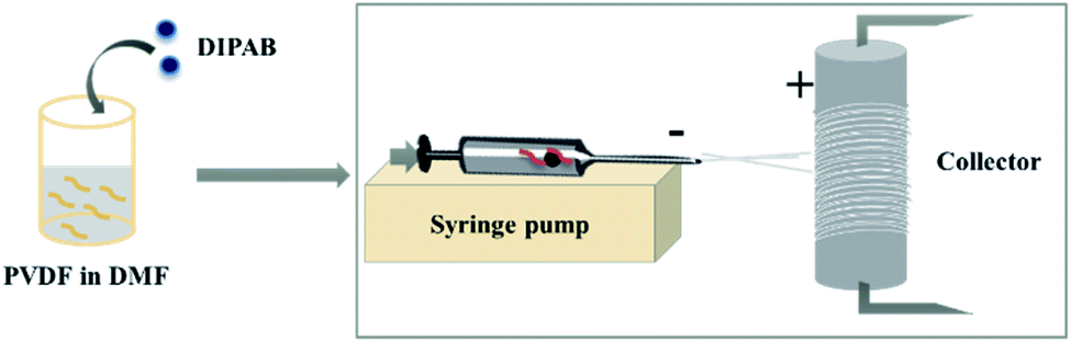
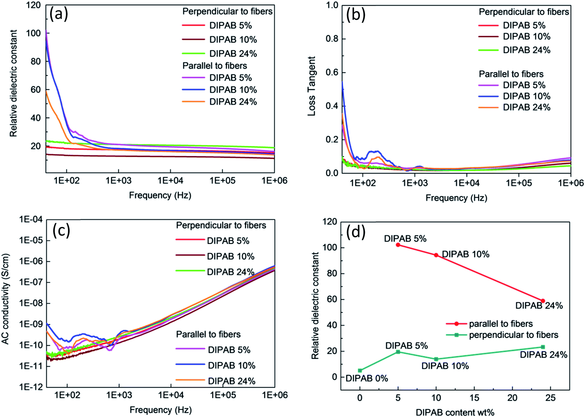
DIPAB doped PVDF solution (10 ml) with a doping ratio 0%, 5%, 10% and 24% by wt were prepared. The following doping ratios were considered based on the previous studies performed on DIPAB doped PVDF thin film samples where the highest dielectric constant was observed in samples below 10 wt% DIPAB doping.9 The sample with highest DIPAB loading (24.2 wt%) was considered based on the improved orientation in doping samples since the above this concentration, the polymer solution became too viscous to electrospin well and it was difficult to maintain the fibers orientation. Each sample was loaded in a plastic syringe fitted with a metallic needle tip (18G). The syringe containing the solution was then loaded on the top of an automatic syringe pump (Harvard Apparatus) and was connected to the high voltage power source (Gamma High Voltage Research) as shown in Fig. 1. The solution was fed to the setup at varying infusion rates and electric fields depending on the DIPAB–PVDF ratio (Table 1). The fibers were collected on an aluminum foil wrapped on a custom made rotating drum (diameter – 7 cm) located at a fixed distance of 7 cm.
 |
| | Fig. 1 Electrospinning setup for DIPAB–PVDF nanofibers. | |
Table 1 Parameters for the electrospinning of PVDF nanofibers with varying DIPAB content by wt%
| S. no. |
Sample label |
DIPAB in PVDF [wt%] |
Infusion rate [ml h−1] |
Voltage applied [kV] |
| 1 |
DIPAB 0% |
0% |
1 |
12 |
| 2 |
DIPAB 5% |
5% |
0.85 |
13 |
| 3 |
DIPAB 10% |
10% |
0.75 |
10.7 |
| 4 |
DIPAB 24% |
24% |
0.85![[thin space (1/6-em)]](https://www.rsc.org/images/entities/char_2009.gif) |
15 |
Characterization
X-Ray diffraction (XRD) was performed on a Panalytical X-ray diffractometer using Cu-Kα at an operating voltage of 45 kV and current of 40 mA at room temperature to study the crystal structure of the nanocomposite fibers. Fourier transform infrared spectra (FTIR) was recorded over a range of 650 to 1000 cm−1 to study the presence of β-phase of PVDF. Scanning electron microscopy (SEM) was performed on a Jeol SEM-6500 microscope to study the morphologies of obtained nanofibers. The samples were coated with Platinum to prevent charging. The XRD, FTIR and SEM were performed on the sheets of aligned PVDF nanofibers with different DIPAB ratios. The dielectric measurements were performed on the same batch of the samples. High resolution transmission electron microscopy (HR-TEM) was further performed using a Jeol TEM-2100F instrument to confirm the uniform doping of DIPAB and observe the formation of DIPAB nanocrystals inside the fibers. The composite nanofibers were spun directly on carbon coated lacey copper grids. The uniform doping of DIPAB was also proven by performing an Energy dispersive X-ray spectroscopic (EDXS) analysis on the sample using the same equipment for SEM imaging. The dielectric properties of the nanofibers were measured using parallel RLC circuit with Agilent 4294A impedance analyser and Agilent 16451B dielectric test fixture at 500 mV for all the measurements. The impedances of nanofibers were measured in the range of 40 Hz to 1 MHz. Smoothening was performed on the collected dielectric data to reduce the noise. The observed noise might have been caused by the improper contact of the electrodes with some nanofibers during the measurements.
Results and discussions
Structural characterization
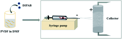
Fig. 2 shows the comparison of X-ray diffraction (XRD) patterns of PVDF nanofibers, DIPAB powder, and DIPAB–PVDF nanofibers. The XRD of the PVDF nanofibers shows a strong diffraction peak at 20.3°, which corresponds to the β-phase of PVDF. No significant non-polar α-phase peak at 18.3° and γ-phase peak at 38.3° of PVDF were observed in the nanofiber samples containing DIPAB. A small peak was observed at 18.3° for the PVDF sample without DIPAB. The peak of the β-phase shifts slightly to 20.42° when it is loaded with DIPAB powder probably because of the interaction of DIPAB with the PVDF structure. These results also confirm the DIPAB incorporation into the PVDF matrix. The α-phase or the 1-F (ferroelectric) phase of DIPAB is clearly visible through the presence of characteristic 2θ peaks in the XRD at 12.5°, 17.0°, 22.4°, 25.2° and 27.6°. These peaks correspond to the monoclinic system of DIPAB crystals.
 |
| | Fig. 2 XRD patterns of PVDF nanofibers, DIPAB and DIPAB–PVDF nanofibers showing the dominating β-phase in DIPAB–PVDF nanofibers sample. | |
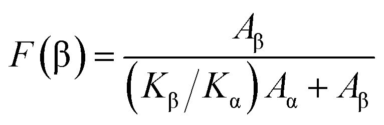
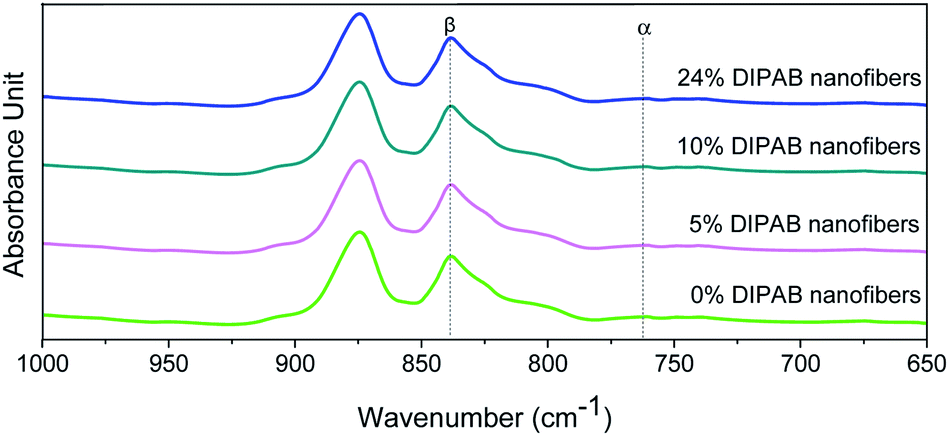
The crystalline structure and β-phase of PVDF nanofibers with different concentrations of DIPAB was investigated by Fourier transform infrared (FTIR) spectroscopy. Fig. 3 shows the FTIR spectra for all the nanofiber structures. The vibration bands at 510 cm−1 (CF2 stretching), 598 cm−1 (CF2 waging) and 840 cm−1, (CF2 asymmetric stretching and CH2 rocking) represent the electroactive β-phase. The electrospinning of nanofibers result to higher β-phase content when it is performed at room temperature (below 80 °C) along with uniaxial stretching at high electric fields. The intense vibration occurring at 840 cm−1 confirms the presence of a very high concentration of the β-phase. The β-phase was calculated for all the nanofibers sample using the equation:
where
Aα and
Aβ are the corresponding wavenumber values at 762 cm
−1 and 840 cm
−1, and the
Kα and
Kβ are the absorption coefficients for the α and β-phases with a value of 6.1 × 10
4 cm
2 mol
−1 and 7.7 × 10
4 cm
2 mol
−1, respectively.
30 The high β-phase of ∼93.8 wt% was observed in all the DIPAB doped PVDF samples.
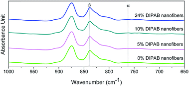 |
| | Fig. 3 FTIR spectra of DIPAB–PVDF composite films for varying weight ratios 0–24% showing the formation of the dominating electroactive β-phase in electrospun nanofibers. | |
The incorporation and dispersion of DIPAB crystals inside the PVDF nanofibers was confirmed using Scanning Electron Microscopy (SEM). Fig. 4(a) shows the SEM micrograph of nanofibers with pure PVDF. The alignment and size distribution of pure PVDF nanofibers were not uniform. Fig. 4(b–d) show that the nanofibers were aligned when 5 wt%, 10 wt% and 24 wt% DIPAB doping was applied. At higher DIPAB concentrations in the PVDF solutions, the fibers' alignment degraded. The alignment issues were corrected by adjusting the infusion rate of polymer solutions and the applied voltage. The studies were performed on four electrospun samples based on the wt% of DIPAB added to the PVDF solution in DMF. The maximum doping of DIPAB in PVDF prior to electrospinning was kept around 24.2 wt% after which it became very difficult to obtain well aligned nanofibers. DIPAB was found to be everywhere in the fibers and not in the background (see ESI†). The signal of nitrogen and bromine confirmed the presence of DIPAB in the nanofibers.
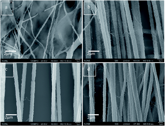 |
| | Fig. 4 SEM micrographs of (a) DIPAB 0%, (b) DIPAB 5%, (c) DIPAB 10% and (d) DIPAB 24% representing alignment in PVDF nanofiber samples doped with DIPAB. | |
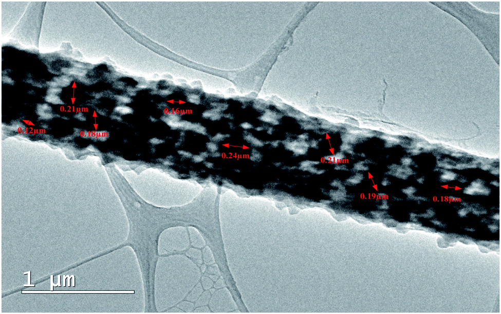
High resolution Transmission Electron Microscopy (TEM) was further performed to confirm the uniform doping of DIPAB in the PVDF nanofibers. Fig. 5 shows the TEM micrograph of a single DIPAB–PVDF nanofiber containing 5 wt% DIPAB. The darker contrast material is DIPAB while lighter contrast is portrayed by semicrystalline PVDF. DIPAB was found to be dispersed equally inside the nanofibers, which creates a large interface between the two materials without any visible agglomeration. The size of the DIPAB nanoparticles formed in situ was in the range of ∼80–250 nm.
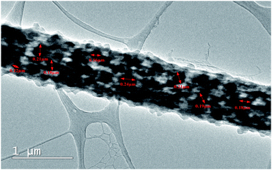 |
| | Fig. 5 TEM micrograph of single DIPAB–PVDF (DIPAB 5%) nanofiber incorporated with nanoparticles of DIPAB. | |
Dielectric and ferroelectric properties
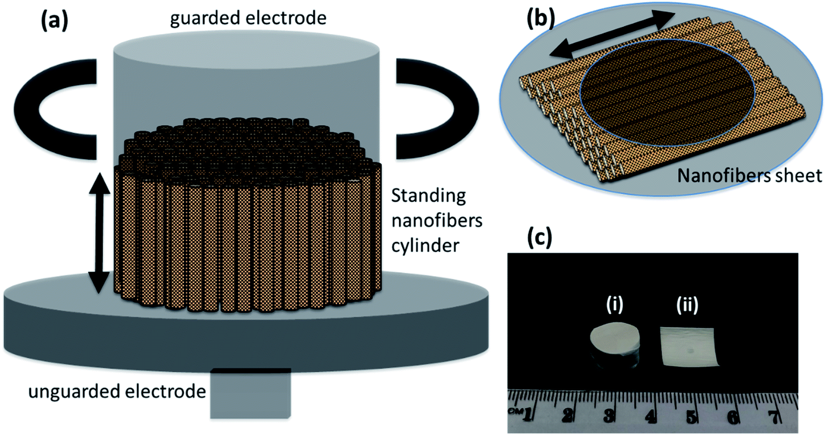
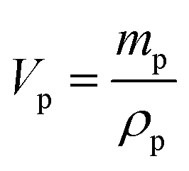
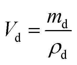
The frequency dependent measurements were performed parallel as well as perpendicular to the nanofibers' orientation. This was done to prove the enhanced performance of nanofibers in the preferred orientation. The measurements parallel to the nanofibers required the formation of a cylinder of standing nanofibers with a height of less than 1 cm—Fig. 6(a). The cylinder of standing nanofibers was formed by stacking multiple sheets of parallel nanofibers on the top of each other. These sheets were obtained by neatly cutting the big electrospunned nanofibers sheet into smaller sheets. The characterisation and measurements were also performed on the same sample. The utmost care was taken that the orientation was preserved in the overall cylinder. The nanofiber sheets were held together and packed carefully from the side using Teflon tape. The diameter of the cylinder of standing nanofibers was bigger than that of the electrode. Therefore, the Teflon tape had no impact during the measurement of the dielectric properties of DIPAB doped PVDF nanofibers. The volume fraction measurements were later performed individually on each sample to provide accurate results. The measurements perpendicular to the nanofibers' orientation were done by placing the nanofiber sheets between the two electrodes of the Agilent 16451B dielectric test fixture—Fig. 6(b). Fig. 6(c) shows a nanofiber cylinder and sheet made by the above method. Care was taken that the nanofiber cylinders retained their shape and alignment during the measurements. This method was chosen to provide more accuracy in the data by using the same electrodes and setup for all the frequency dependent measurements. Since all of the samples were spun at different infusion rates, we expected them to have different thicknesses when in sheet form. The height of the cylinders was also carefully measured. Table 2 shows the thicknesses and heights of the film samples and cylinder samples, respectively.
 |
| | Fig. 6 Schematic for electrical measurements, (a) cylinder of standing electrospunned nanofibers in between dielectric test fixture (Agilent 16451B) electrodes for dielectric measurements parallel to the length, (b) sheet of nanofibers for dielectric measurements perpendicular to the length, and (c) real life sample for dielectric measurements (i) nanofibers cylinder (ii) nanofibers sheet. | |
Table 2 Representation of the thickness (d) in mm for DIPAB–PVDF nanofibers samples for dielectric measurements
| S. no. |
Sample name |
Thickness (d) [mm] |
| 1 |
DIPAB 5% film |
0.17 |
| 2 |
DIPAB 10% film |
0.12 |
| 3 |
DIPAB 24% film |
0.20 |
| 4 |
DIPAB 5% cylinder |
1.30 |
| 5 |
DIPAB 10% cylinder |
1.22 |
| 6 |
DIPAB 24% cylinder |
6.30 |
The capacitance (C), loss tangent (tanδ), admittance magnitude (Y) and phase (θ) of the samples were measured to calculate the relative dielectric constant (εr) and the AC conductivity (σAC) using the following equations:
| | | σAC = Ydcos(θ)/A | (2) |
where,
d and
A represent the thickness and area of the samples, respectively, and
ε0 is the constant vacuum permittivity with a value of 8.854 × 10
−12 F m
−1.
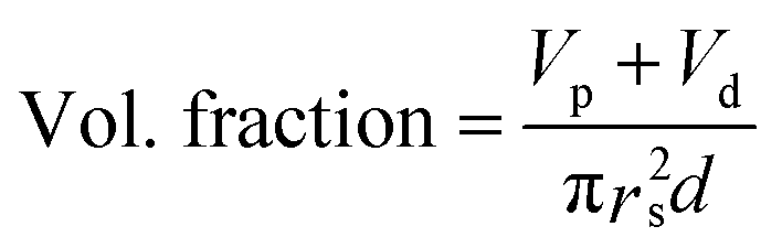
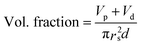
The dielectric values were calculated based on the volume fraction of electrospun nanofibers as the nanofiber sheets had voids in them. Eqn (10) was used to calculate the volume fraction of nanofibers during the measurements and the actual relative dielectric constant was measured using eqn (11). These equations were derived using eqn (3)–(9).
| |  | (6) |
| |  | (7) |
| |  | (10) |
| |  | (11) |
mf,
mp and
md are the masses, and
Vf,
Vp and
Vd are the volumes of electrospun nanofibers, PVDF and DIPAB, respectively.
Vs is the overall volume of the samples.
εrc is the corrected relative dielectric constant of the sample (
eqn (11)).
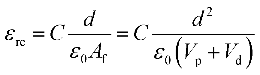
The frequency dependent properties of DIPAB doped PVDF nanofibers with varying DIPAB content ratio at room temperature in the range of 40 Hz to 1 MHz is shown in Fig. 7. DIPAB doped PVDF nanofibers showed an enhanced dielectric constant in comparison to the previously reported dielectric constants for pure PVDF nanofibers which were in the range of 11 to 18 at low frequencies.31–33Fig. 7(a) shows the variations in the dielectric constant of PVDF nanofibers doped with varying ratios of DIPAB. The data shows a decrease in dielectric constant with increasing frequency in all of the nanofiber samples due to the decreasing effective number of dipoles.34,35 The dipoles' oscillations at lower frequencies are in sync with the alternating field, while at higher frequencies they are not. This results in a reduction in the effective number of dipoles. The DIPAB nanocrystals dispersion inside the PVDF nanofibers results to large interfacial area between the two materials. Due to the large difference in the electrical conductivities of PVDF and DIPAB, the charges can migrate and accumulate at the interface of the materials on the application of the electric field. This results in interfacial polarisation, and hence a relatively high dielectric constant.36 With increasing DIPAB content, the inter-particle distance decreases and the interfacial area per unit mass increases.37 This results in the improvement of the average polarisation associated with the coupling between neighboring grains leading to a significantly higher dielectric enhancement of the composite nanofibers. However, this is true only at low concentrations of DIPAB doping (<5 wt%). The interfacial polarisation works smoothly at lower frequencies as the charges have enough time to move. At higher frequencies, the mismatch between frequency and charge carrier movements results in a decrease in dielectric constant.38 The dielectric constant was also affected positively when DIPAB was added to PVDF because of the highly ionic nature of the DIPAB crystals that contributed to the dielectric constant by ionic polarisation.
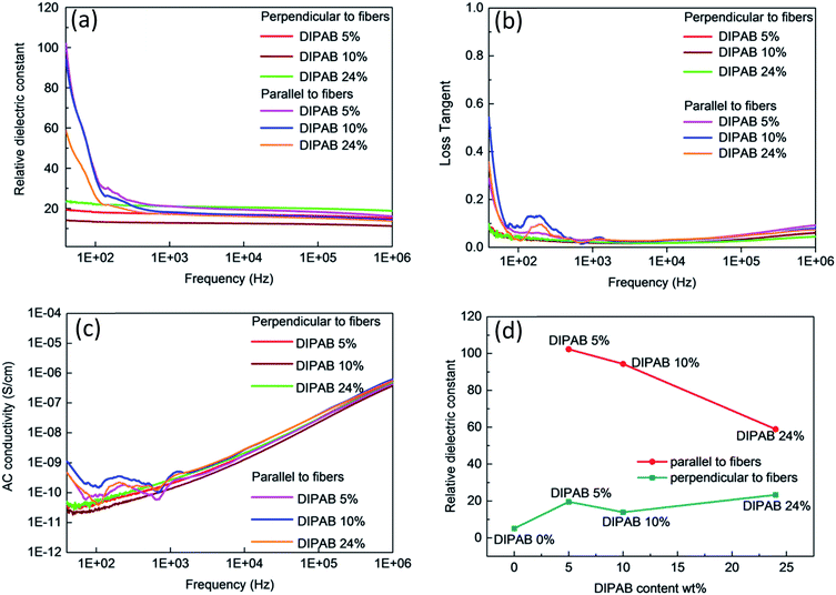 |
| | Fig. 7 Frequency dependent dielectric properties of DIPAB–PVDF nanofibers: (a) dielectric constant, (b) loss tangent (c) AC conductivity, (d) DIPAB content dependence of dielectric constant of DIPAB–PVDF nanofibers. | |
The two-way relative dielectric constant measurements (parallel as well as perpendicular to the nanofibers) were undertaken to prove the alignment of dipoles along the direction of the nanofibers. During the electrospinning process, the PVDF nanofibers were spun under a very high applied voltage (ranging from 10 kV to 17.5 kV). This resulted in the poling in the PVDF structure where the alignment of the dipoles is along the direction of spinning of nanofibers that cause an increase in the effective dipole moment in these structures. This phenomenon is known as orientation polarisation. It can be seen from Fig. 5 that addition of DIPAB to the PVDF has resulted in very well aligned nanofibers which increased effective dipole moments along the length or parallel to the nanofibers, and hence higher relative dielectric constants.
The maximum dielectric constant recorded was ∼102 in 5 wt% DIPAB doped PVDF (DIPAB 5%) nanofiber samples when the measurements were performed parallel to the nanofibers. To the best of our knowledge, this was by far the highest value ever recorded for this composite material. The dielectric value when measured perpendicular to the nanofibers was much lower (∼19 at 40 Hz) for the DIPAB 5% sample. This proves that most of the dipoles present in the nanofibers were contributing to the dielectric behavior of nanofibers in the direction along the length of the nanofibers showing the effect of orientation polarisation. The values are lower in all the samples when measured perpendicular to nanofibers and they followed the trend like other nanofibers with increasing frequency. It is expected that dielectric constant should increase with the increase in the doping of DIPAB in the PVDF nanofibers owing to the high spontaneous ionic polarisation of DIPAB. The dielectric constant of DIPAB 5 wt% sample was observed to be the highest at low frequencies as a result of the formation of DIPAB nanoparticles that are equally dispersed in the nanofibers. Fig. 7(a) shows the dielectric constant of the higher DIPAB doped samples (e.g. DIPAB 24%) to be lower than DIPAB 5% sample. This can be attributed to the formation of in larger DIPAB particles at higher doping. The increased DIPAB particle size results to decreased surface to volume ratio and hence decreased surface area between the two materials. The decreased surface area resulted to a lower interfacial polarisation as it directly dependent on the interface area. The dielectric constant should increase with the increasing DIPAB concentration since DIPAB has relatively higher εr but the decreasing trend of εr proved that the ionic polarisation was dominated by the interfacial polarisation. This proves domination of interfacial polarisation at low frequencies. The ionic polarisation exceeds the interfacial polarisation at high DIPAB concentration. This can be confirmed by the dielectric measurements performed perpendicular to the alignment of the nanofibers. The dielectric constant was found to be highest in the DIPAB 24% sample. The dielectric measurements performed parallel to the nanofibers proved that interfacial polarisation play a huge role in enhancing the dielectric properties. The ionic and interfacial polarisation can usually be attributed to the distinguishable dielectric loss factor peaks. However, the complex network of DIPAB–PVDF in this work cannot be represented by a simple model and the specific dielectric loss factor peaks associated with different polarisations could not be plotted. The individual fibers and the conjunction between the fibers corresponded to multiple peaks where individual peaks were indistinguishable from each other. Overall, the dielectric constant is most effected by orientation of dipoles followed by the interfacial polarisation as a result of charge trapping followed by the ionic polarisation.
The loss tangent vs. frequency values are shown in Fig. 7(b). The loss tangent values decreased with increasing frequency as expected due to the Maxwell–Wagner–Sillars effect.28 The DIPAB 5% sample had a loss tangent of 0.3 at 40 Hz parallel to the nanofibers. The highest loss tangent of 0.55 was shown by the DIPAB 10% sample at low frequency. The loss tangent for all the samples measured perpendicular to the nanofibers' orientation was very low (<0.1). The loss tangent tends to increase at higher frequency, which is caused by conductance. The AC conductivity increased with increasing frequency as shown in Fig. 7(c). It was found to be highest in the DIPAB 10% sample with a value of 1.1 × 10⁻⁹ S cm−1 at 40 Hz. The DIPAB 5% sample had an AC conductivity of 0.43 × 10⁻⁹ S cm−1 at 40 Hz. The bump in the dielectric constant, loss tangent and AC conductivity data for all the samples was observed in the range of 100 Hz to 500 Hz when the measurements were performed parallel to the nanofibers. These features are constant in all the sample which proves that it is not the noise. It could be the result of complex pathways formation in the composite structure. The limit of detectability of the impedance analyser, for example, the AC conductivity measurements where the value is as low as 2.2 × 10⁻¹⁰ S cm−1 for DIPAB 5% sample makes it difficult to conclude the real reason for the above feature. Fig. 7(d) shows the comparison of relative dielectric constants of all the fibers parallel and perpendicular to the nanofibers for varying DIPAB doping in the nanofibers at 40 Hz. The DIPAB 5% sample had the highest relative dielectric constant. The value of εr decreased gradually with an increasing amount of DIPAB doping. The values of εr, when measured perpendicular to the nanofibers, were very low for the same fibers because of a very low number of effective dipoles. This also proves that the orientation polarisation and presence of DIPAB play a significant role in the enhancement of the dielectric properties of the material.
Conclusions
For the first time DIPAB, which is a highly ferroelectric compound was successfully dispersed in PVDF nanofibers. The electrospinning and addition of DIPAB helped to obtain very high β-phase, improved alignment and crystallinity in the fibers in comparison to the thin-film samples. The dielectric properties were significantly improved and by far the highest relative dielectric constant was observed in this composite material. Incorporating DIPAB in PVDF is an effective way to produce anisotropic and highly dielectric nanofibers that may be ideal candidates for applications such as electric-energy-storage capacitors and actuators.
Conflicts of interest
There are no conflicts to declare.
Acknowledgements
The authors would like to thank David Flynn from the School of Chemical and Physical Sciences, Victoria University of Wellington, Wellington for his help with SEM analysis. Furthermore, they thank Dr Gideon Gouws of the School of Engineering and Computer Science, Victoria University of Wellington, Wellington for his help with the electric measurements.
Notes and references
- J. Valasek, Phys. Rev., 1921, 17, 475–481 CrossRef CAS.
- P. Potnis, N.-T. Tsou and J. Huber, Materials, 2011, 4, 417–447 CrossRef CAS.
- N. Setter, D. Damjanovic, L. Eng, G. Fox, S. Gevorgian, S. Hong, A. Kingon, H. Kohlstedt, N. Y. Park, G. B. Stephenson, I. Stolitchnov, A. K. Taganstev, D. V. Taylor, T. Yamada and S. Streiffer, J. Appl. Phys., 2006, 100, 051606 CrossRef.
- N. Murayama, K. Nakamura, H. Obara and M. Segawa, Ultrasonics, 1976, 14, 15–24 CrossRef CAS.
- B. Ploss, B. Ploss, F. G. Shin, H. L. W. Chan and C. L. Choy, IEEE Trans. Dielectr. Electr. Insul., 2000, 7, 517–522 CAS.
- C. R. Bowen, H. A. Kim, P. M. Weaver and S. Dunn, Energy Environ. Sci., 2014, 7, 25–44 RSC.
- W. Qin, B. Xu and S. Ren, Nanoscale, 2015, 7, 9122–9132 RSC.
- A. S. Tayi, A. Kaeser, M. Matsumoto, T. Aida and S. I. Stupp, Nat. Chem., 2015, 7, 281–294 CrossRef CAS.
- Y. Sui, W.-T. Chen, J.-J. Ma, R.-H. Hu and D.-S. Liu, RSC Adv., 2016, 6, 7364–7369 RSC.
- K. Han, Q. Li, C. Chanthad, M. R. Gadinski, G. Zhang and Q. Wang, Adv. Funct. Mater., 2015, 25, 3505–3513 CrossRef CAS.
- J. Y. Lim, S. Kim and Y. Seo, AIP Conf. Proc., 2015, 1664, 070006 CrossRef.
- B. Hilczer, J. Kułek, E. Markiewicz, M. Kosec and B. Malič, J. Non-Cryst. Solids, 2002, 305, 167–173 CrossRef CAS.
- A. V. Shirinov and W. K. Schomburg, Sens. Actuators, A, 2008, 142, 48–55 CrossRef CAS.
- R. Pérez, M. Král and H. Bleuler, Sens. Actuators, A, 2012, 183, 84–94 CrossRef.
- M. Zirkl, A. Sawatdee, U. Helbig, M. Krause, G. Scheipl, E. Kraker, P. A. Ersman, D. Nilsson, D. Platt, P. Bodö, S. Bauer, G. Domann and B. Stadlober, Adv. Mater., 2011, 23, 2069–2074 CrossRef CAS.
- S. J. Kang, Y. J. Park, I. Bae, K. J. Kim, H.-C. Kim, S. Bauer, E. L. Thomas and C. Park, Adv. Funct. Mater., 2009, 19, 2812–2818 CrossRef CAS.
- D. M. Esterly and B. J. Love, J. Polym. Sci., Part B: Polym. Phys., 2004, 42, 91–97 CrossRef CAS.
- S. K. Mahadeva, J. Berring, K. Walus and B. Stoeber, J. Phys. D: Appl. Phys., 2013, 46, 285305 CrossRef.
- Y. Ahn, J. Y. Lim, S. M. Hong, J. Lee, J. Ha, H. J. Choi and Y. Seo, J. Phys. Chem. C, 2013, 117, 11791–11799 CrossRef CAS.
- W. Zhou, Q. Chen, X. Sui, L. Dong and Z. Wang, Composites, Part A, 2015, 71, 184–191 CrossRef CAS.
- S. Liu, S. Xue, W. Zhang, J. Zhai and G. Chen, J. Mater. Chem. A, 2014, 2, 18040–18046 RSC.
- F. Liu, Q. Li, J. Cui, Z. Li, G. Yang, Y. Liu, L. Dong, C. Xiong, H. Wang and Q. Wang, Adv. Funct. Mater., 2017, 27, 1606292 CrossRef.
- I. Bergenti, G. Ruani, F. Liscio, S. Milita, F. Dinelli, X. Xu, E. Wang and M. Cavallini, Langmuir, 2017, 33, 12859–12864 CrossRef CAS.
- D.-W. Fu, H.-L. Cai, Y. Liu, Q. Ye, W. Zhang, Y. Zhang, X.-Y. Chen, G. Giovannetti, M. Capone, J. Li and R.-G. Xiong, Science, 2013, 339, 425–428 CrossRef CAS PubMed.
- S. Poddar, H. Lu, J. Song, O. Goit, S. Valloppilly, A. Gruverman and S. Ducharme, J. Phys. D: Appl. Phys., 2016, 49, 505305 CrossRef.
- N. Nuraje and K. Su, Nanoscale, 2013, 5, 8752 RSC.
- L. Huang, Z. Chen, J. D. Wilson, S. Banerjee, R. D. Robinson, I. P. Herman, R. Laibowitz and S. O'Brien, J. Appl. Phys., 2006, 100, 034316 CrossRef.
- W. Yang, H. Li, J. Lin, G. Chen, Y. Wang, L. Wang, H. Lu, L. Chen and Q. Lei, J. Mater. Sci.: Mater. Electron., 2017, 28, 9658–9666 CrossRef CAS.
- A. Baji, Y.-W. Mai, Q. Li and Y. Liu, Nanoscale, 2011, 3, 3068 RSC.
- S. Florczak, T. Lorson, T. Zheng, M. Mrlik, D. W. Hutmacher, M. J. Higgins, R. Luxenhofer and P. D. Dalton, Polym. Int., 2019, 68, 735–745 CrossRef CAS.
- H. H. Park, Y. Choi, D. J. Park, S. Y. Cho, Y. S. Yun and H.-J. Jin, Fibers Polym., 2013, 14, 1521–1525 CrossRef CAS.
- M. Abbasipour, R. Khajavi, A. A. Yousefi, M. E. Yazdanshenas and F. Razaghian, J. Mater. Sci.: Mater. Electron., 2017, 28, 15942–15952 CrossRef CAS.
- A. Issa, M. Al-Maadeed, A. Luyt, D. Ponnamma and M. Hassan, C, 2017, 3, 30 Search PubMed.
- J. Pu, Y. Yomogida, K.-K. Liu, L.-J. Li, Y. Iwasa and T. Takenobu, Nano Lett., 2012, 12, 4013–4017 CrossRef CAS PubMed.
- A. C. Lopes, C. M. Costa, R. S. i Serra, I. C. Neves, J. L. G. Ribelles and S. Lanceros-Méndez, Solid State Ionics, 2013, 235, 42–50 CrossRef CAS.
- P. Lunkenheimer, V. Bobnar, A. V. Pronin, A. I. Ritus, A. A. Volkov and A. Loidl, Phys. Rev. B, 2002, 66, 052105 CrossRef.
- P. Thakur, A. Kool, B. Bagchi, S. Das and P. Nandy, Phys. Chem. Chem. Phys., 2015, 17, 1368–1378 RSC.
- R. G. Lorenzini, W. M. Kline, C. C. Wang, R. Ramprasad and G. A. Sotzing, Polymer, 2013, 54, 3529–3533 CrossRef CAS.
Footnote |
| † Electronic supplementary information (ESI) available. See DOI: 10.1039/c9ra06470b |
|
| This journal is © The Royal Society of Chemistry 2019 |
Click here to see how this site uses Cookies. View our privacy policy here. 
 Open Access Article
 This Open Access Article is licensed under a
  a,
Mohsen
Maddah
a,
Mohsen
Maddah