DOI:
10.1039/C9RA06381A
(Paper)
RSC Adv., 2019,
9, 31840-31845
Optimization of the thermoelectric performance of layer-by-layer structured copper-phthalocyanine (CuPc) thin films doped with hexacyano-trimethylene-cyclopropane (CN6-CP)†
Received
15th August 2019
, Accepted 27th September 2019
First published on 7th October 2019
Abstract
Copper-phthalocyanine (CuPc), as a classical small molecular organic semiconductor, has been applied in many fields. However, the low intrinsic conductivity limits its application in thermoelectricity. Here, hexacyano-trimethylene-cyclopropane (CN6-CP), a strong electron acceptor, is synthesized as dopant for CuPc thin films to improve their conductivities. Multilayer thin films constructed from alternate thermally evaporated CuPc and CN6-CP thin layers are investigated. Under the optimized condition, the doped CuPc film with a conductivity of 0.76 S cm−1 and a Seebeck coefficient of 130 μV K−1, shows a high power factor of 1.3 μW m−1 K−2 and the carrier concentration is estimated to be 2.8 × 1020 cm−3. Considering the relatively superior performance, the CN6-CP doped CuPc film is a promising small molecular organic thermoelectric (OTE) material. In addition, for those highly crystalline materials with poor solubility, the layer-by-layer structure offers a general strategy for investigation and optimization of their TE performance.
Introduction
Recently, organic thermoelectric (OTE) materials, which convert thermal energy and electricity, are of huge interest.1–3 The figure of merit ZT was established to evaluate the TE performance:where T, σ, κ, and S are absolute temperature, electrical conductivity, thermal conductivity, and Seebeck coefficient, respectively. As organic compounds generally have low value thermal conductivities, the main evaluation criterion for OTE materials is the value of the power factor PF, PF = S2σ.4 Therefore, enhancement of electrical conductivity as well as maintaining the Seebeck coefficient value is important for OTE materials.5 Some polymeric systems which potentially have high TE performances have been reported,1,2,6 but small-molecule based OTE materials have so far rarely been addressed.7 Due to the wide variety of small-molecule organic semiconductor materials and their obvious advantages in synthesis, characterization and crystal growth, their TE properties still need to be investigated extensively and in depth.
Metallic Phthalocyanines (MPcs), which are well known for their excellent chemical and thermal stability, is a versatile class of organic semiconducting materials with attractive charge transport and optical properties.8–11 Early studies reported that the Seebeck coefficient of pristine MPcs falls into the range of 0.9–1.8 mV K−1,12 and the Hall measurement demonstrated that the mobility in single crystal MPcs is on the order of 1 cm2 V−1 s−1.13 The highest field-effect mobility of holes in thin films of TiOPc is reported to be 10 cm2 V−1 s−1.14 The high charge carrier mobilities and the large Seebeck coefficients suggest that MPcs could have promising TE properties. Additionally, theoretical simulations carried out by Shuai et al.15 revealed the close relationship between carrier concentration and TE properties of MPcs. Their work predicts the ZT value of NiPc may reach marvellous 2.5 at particular carrier concentration.15,16
Here, we chose CuPc as the p-type TE materials. Since pristine CuPc are intrinsic semiconductor, charge carriers must be externally provided by means of doping. A stronger electron acceptor is needed for doping CuPc efficiently. CN6-CP was originally synthesized in the 1970s17,18 and was recently identified as a promising molecular dopant by Karpov et al.19 With an EA of −5.87 eV, this is the strongest p-type small-molecular dopant for organic semiconductor yet reported in the literature.17–19 We made CN6-CP as the dopant for improving the carrier concentration of CuPc films. Multilayer thin films constructed by alternately thermal evaporated CuPc and CN6-CP thin layers were investigated. Under the optimized condition, the corresponding conductivity and Seebeck coefficient can be up to 0.76 S cm−1 and 130 μV K−1, respectively. Thus, a high power factor of 1.3 μW m−1 K−2 can be obtained, which is the highest value ever reported for CuPc films. Combining the mobility derived from the corresponding FET devices and conductivities measured, the carrier concentrations is estimated to be 2.8 × 1020 cm−3 for the doped CuPc films. Compare to the intrinsic CuPc films, the conductivity of doped CuPc films has remarkably improved. It shows relatively superior TE performance and broadens the range of small molecular OTE materials. In addition, the layer-by-layer structure provides a general opportunity for investigation and optimization of the TE performance for those highly crystalline materials with poor solubility.
Experimental
Materials
CuPc was purchased from Sigma-Aldrich and purified by sublimation for two times. CN6-CP was synthesized following a reported procedure.19
Film preparation and doping process
The samples are prepared by thermal evaporation in high vacuum chambers (6 × 10⁻⁴ Pa) driven by turbo molecular pumps. The material is evaporated from fused silica crucibles onto substrates and the rate for CuPc and CN6-CP is 0.6 nm min−1 and 0.3 nm min−1, respectively.
Film characterization
The ultraviolet-visible-near-infrared (UV-vis-NIR) absorption spectra are obtained from V-570 UV/vis/NIR spectrometer (JASCO Inc.). The morphologies are measured by atomic force microscopy (AFM) in tapping mode (Nanoscope IV Digital Instruments, Bruker). The X-ray diffraction (XRD) spectra were obtained from the Rigaku D X-ray diffractometer with Cu Kα radiation. X-ray Photoelectron Spectrum (XPS) and Ultraviolet Photoelectron Spectrum (UPS) were obtained by using an AXIS Ultra-DLD ultrahigh vacuum photoemission spectroscopy system (Kratos Co.). A monochromatic aluminium Kα source (1486.6 eV) was used for XPS and a He I source (21.22 eV) was used for UPS. All characterizations were performed under ultra-high-vacuum (3 × 10⁻⁹ Torr).
The measurement of OFETs of pristine and doped CuPc films
OFETs with a bottom-gate/bottom-contact configuration were constructed on the substrate of highly doped silicon with 300 nm of SiO2 as the dielectric layer. The source-drain gold electrodes are evaporated in a vacuum chamber by a shadow mask. The channel length and width were 50 μm and 1400 μm, respectively. The SiO2/Si substrate was cleaned by distilled water, ethanol, and acetone and dry with nitrogen. Then it dips in piranha solution (a mixture of 30 vol% H2O2 and 70 vol% H2SO4), followed by O2 plasma treatment. Finally, it is modified with a self-assembled monolayer (SAM) of octadecyltrichlorosilane (OTS). Multilayer CuPc films with different doping concentration were deposited on OTS-modified substrate via thermal evaporation. The evaporation rate is 0.6 nm min−1 for CuPc and 0.3 nm min−1 for CN6-CP with the substrates kept at ambient temperature. The performances of OFETs are measured with a Keithley 4200 SCS.
The measurement of TE property
The glass substrates were cleaned by distilled water, ethanol, and acetone and dry with nitrogen. Then it dips in piranha solution (a mixture of 30 vol% H2O2 and 70 vol% H2SO4), followed by O2 plasma treatment. Finally, it is modified with a SAM of OTS. CuPc and CN6-CP were evaporated alternately on OTS-modified substrate and adjust the thickness of CN6-CP to alter the doping concentration. The evaporating rate for CuPc and CN6-CP is 0.6 nm min−1 and 0.3 nm min−1, respectively. The gold electrodes are evaporated onto the glass substrate in a vacuum chamber by a shadow mask. The channel length and width were 500 μm and 5000 μm, respectively. Conductivity was measured with Keithley 4200 SCS by a four-probe method. The Seebeck coefficient can be obtained by the formula:n
The temperature difference ΔT was created by two Peltier modules. We fix the two Peltier modules, and then apply a voltage to one module. As a result, it will generate a certain temperature difference and that corresponds to the voltage. The temperature difference can be obtained from two resistive thermometers and the thermal voltage Vthem is measured by Keithley 4200 SCS. Besides, the conductivity and Seebeck coefficient are recorded in the same device.
Results and discussion
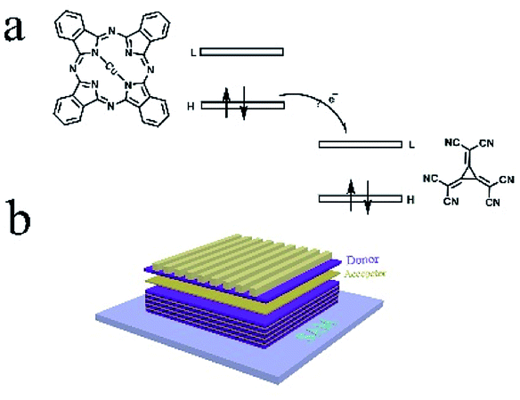
The molecular structure of CuPc and CN6-CP is show in Fig. 1a. The highest occupied molecular orbital (HOMO) level of CuPc is −4.80 eV and the lowest unoccupied Molecular Orbital (LUMO) level of CN6-CP is −5.87 eV. The energy offset between the HOMO of CuPc and LUMO of CN6-CP is sufficient to drive the electron transfer from the donor molecules to the acceptors.19,20 Considering the co-evaporation will lead poor ordering of the microstructure of CuPc and decrease the mobility of CuPc film, which will lower the thermoelectric performance, multilayer structure were constructed by depositing CuPc and dopant alternatively to form a layer-by-layer structure (as illustrated in Fig. 1b). The charge transfer between CuPc and dopant molecules happens at the interface between CuPc and CN6-CP layers, while the CuPc layers retain the crystallinity similar to its pristine state which provides the efficient electronic transport path for achieving a higher conductivity comparing to that of the co-sublimated films. So, the conductivity will be mainly determined by the contacting area between the CuPc layers and the dopant layers.
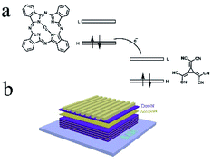 |
| | Fig. 1 (a) The molecular structure and relative energy level of frontier molecular orbitals of CuPc and CN6-CP, (b) the illustration of multilayer structure constructed by alternately thermal evaporated CuPc (donor) and CN6-CP (acceptor) thin layers. | |
Screening of the film formation conditions including film structure, substrate surface modification, total thickness of the CuPc layer and doping concentration
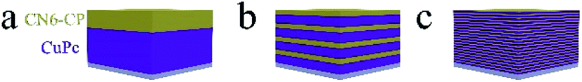
The thin films that we present here can be described with a general formula of (TM CuPc/TD CN6-CP) × LN (TM and TD refer to the thickness of the monolayer of CuPc and CN6-CP and LN refer to the number of repeated CuPc/CN6-CP bilayers). When the total thickness of CuPc TM-total = TM × LN maintained at a constant value, a higher conductivity can be expected for the film with smaller TM and larger LN, as more CuPc molecules locate at the CuPc/CN6-CP interface to interact with the dopant molecules for carrier generation. This expectation is confirmed with a comparison investigation. We construct three multilayer CuPc/CN6-CP films on bare glass substrate with the same TM-total = 40 nm and TD-total = 8 nm (as shown in Fig. 2), but a different LN (LN = 1, 4 and 20 for device 1, 2 and 3). The total CN6-CP/CuPc molecular ratios (MR) in the three devices are equal, as the same total thickness of CuPc and CN6-CP layers present in these films. A drastic increase in electrical conductivity can be observed with lessening the thickness of each CuPc layer. The conductivity of the bilayer thin film displays the lowest of value of 0.002 S cm−1, it increase to 0.12 and 0.3 S cm−1 for the eight-layer and forty-layer films (the results were summarized in Table S1†). This observation shows that the more contact area between CuPc and CN6-CP layer, the more CuPc molecules can be converted into the corresponding cations and serve as charge carriers. So, a multilayer structure with alternatively deposited semiconductor and dopant molecules is an effective method for constructing thin films of doped small molecular semiconductors. And the charge carrier concentration depends on the interface area ratio.
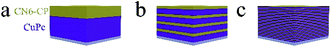 |
| | Fig. 2 The structures of three different device. (a): device 1: (40 nm CuPc/8 nm CN6-CP) × 1, (b): device 2: (10 nm CuPc/2 nm CN6-CP) × 4, (c): device 3: (2 nm CuPc/0.4 nm CN6-CP) × 20. | |
It is well known that the surface state of the substrate has critical impact on the structural ordering of organic semiconductor to be deposited on.21,22 So, for further optimizing the thermoelectric properties of CuPc films, the glass substrates were modified with SAM of OTS,23 (1H,1H,2H,2H-heptadecafluorodecyl)trichlorosilane,24 octadecylphosphonic acid,25 hexamethyldisilazane,26 and poly(amic acid),27 respectively. We constructed multilayer devices with the structure of (2 nm CuPc/0.4 nm CN6-CP) × 20 on the modified substrates. As show in Table S2,† the SAMs have a significant influence on the conductivities of CuPc films, and the OTS-modified substrate is superior to others. As a result, the conductivity increased from 0.3 S cm−1 for film on bare glass substrate to 0.5 S cm−1 for film on OTS-modified substrate. The AFM images show that the pristine CuPc films deposit on OTS-modified glass substrate (Fig. S1†) display enlarged grain size compared to the films deposited on bare glass substrate, corresponding to the improved crystallinity of CuPc films, which will lead to the increase of carrier mobility and hence the enhancement of electrical conductivity.
It is found that for thin films with a structure of (2 nm CuPc/0.4 nm CN6-CP) × LN, when the LN decrease from 20 (total thickness of CuPc layers is 40 nm) to 5 (with total thickness of CuPc layers is 10 nm), the electrical conductivity increases from 0.50 S cm−1 to 0.78 S cm−1 and the Seebeck coefficient (∼120 μV K−1) shows no obvious change. As thermal evaporated CN6-CP thin films are totally amorphous (no diffraction pattern of CN6-CP can be observed in the XRD data of CuPc/CN6-CP films as shown in the following section), the crystallinity of CuPc layers deposited on CN6-CP decrease compared to the films deposited directly on the glass substrates. And this situation gets worse for films with a larger layer number. Based on these pre-screening investigations, we choose the films structure of (2 nm CuPc/TD CN6-CP) × 5 for further optimization of the TE performance via varying the doping concentration, which can be realized by change the TD value, the monolayer thickness of dopant part.
Optimization of TE performance through adjusting of the doping concentration
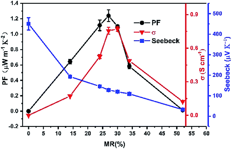
Finally, multilayer thin films with repeated CuPc/CN6-CP bilayer structures on OTS-modified glass substrate with the total thickness of CuPc of 10 nm are fabricated, in which the thickness of each CuPc layer is 2 nm and the doping concentration was varied by changing the thickness of each CN6-CP layer from 0.1 nm to 0.8 nm. As the monolayer thickness of CN6-CP layers is close to the detecting limit of quartz micro-balance, it is difficult to derive the MR between dopant and CuPc via the film thickness monitored by the quartz micro-balance. Here, the MR values were estimated by fitting the XPS spectra of C1s to two parts, the CuPc and CN6-CP molecules, which was shown in Fig. S5† (the data were summarized in Table S3†). The conductivities measurement of the corresponding thin films show that the conductivity increases with the doing concentration and reach a maximum value of 0.78 S cm−1 under a MR of 30% corresponding to thin film with TD = 0.4 nm. Then, the conductivity decreases with further increasing of MR value. The Seebeck coefficients continuously decrease with the increase of MR value (Fig. 3). Under the optimized condition, MR = 27% (TD = 0.3 nm), the corresponding conductivity and Seebeck coefficient can be up to 0.76 S cm−1 and 130 μV K−1, respectively. Thus, a high power factor of 1.3 μW m−1 K−2 is obtained. The continuous decrease of Seebeck coefficient corresponding to an increase of carrier concentration when more CN6-CP molecules are presented in between the CuPc layers, although the contacting areas between CuPc/CN6-CP layers are equal for these multilayer films. This is due to the fact that, when less CN6-CP molecules (such as the film with MR = 14%) are deposited on CuPc film, it could not fully cover the surface of CuPc layer, and the effective interface between CuPc/CN6-CP is small than the area of CuPc deposited. So, more CN6-CP will go to contact with CuPc molecule when the coverage gets increased with more CN6-CP molecules evaporated. The mutual diffusion between the CuPc and CN6-CP layer may contribute to the further increase of carrier concentration after the fully covering of the CuPc layer.
 |
| | Fig. 3 Thermoelectric properties of multilayer CuPc films doped by CN6-CP with the total thickness of CuPc of 10 nm. The performances are optimized by adjusting the CN6-CP/CuPc molecular ratio. | |
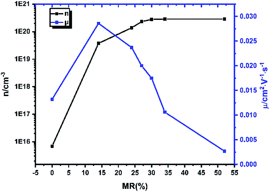
Tuning of the charge carrier concentration is the most general strategy for optimization of the TE performance, not only for inorganic material but also for organic semiconductors. For organic semiconductor, the doping process is critical for carrier generation, which relies on efficient charge transfer between the semiconducting molecules and dopant molecules. For extracting the carrier density of pristine and doped CuPc films, thin film transistors (TFTs) based on CuPc films are constructed and characterized. The TFTs characterization data are shown in Fig. S2 and S3.† For TFTs based on pristine CuPc film, the output curve displays typical saturation region. And the mobility is extracted with the data in the saturation region (VDS > (VGS − Vth)) by applying the following equation:28
| | | IDS = W/2LμCi(VGS − Vth)2 | (3) |
For the CN6-CP doped CuPc films, no saturation region can be observed. The mobility is extracted with the data of linear region (VDS < (VGS − Vth)) according to the equation:
| | | IDS = W/LμCi(VGS − Vth)VDS | (4) |
where
μ is field-effect mobility,
IDS is source-drain current,
Ci is the capacitance per unit area of the gate dielectric layer,
VDS is drain-source voltage,
Vth is threshold voltage,
VGS is gate-source voltage, and
L and
W are the channel length and width, respectively.
28 As shown in
Fig. 4, compared to the pristine CuPc films, the mobilities of the doped films with the lowest MR ratio display a significant increase of carrier mobility, which should be due to the filling of trap states,
29 while the structural ordering maintain at the same level. The mobility decreases with further increasing of doping concentration. This is due to the fact that increasing of the thickness of amorphous CN6-CP layer leads to structural disorder of CuPc deposited on it, which was confirmed by the XRD data (
Fig. 6) and AFM images (Fig. S6
†). The FET mobility (
μ) was used to deduce the charge carrier density combining with the conductivity measured (
σ) (
Fig. 3) according the
eqn (5):
30
 |
| | Fig. 4 The mobility and density of charge carrier of doped CuPc films with different CN6-CP/CuPc MR value. | |
As shown in Fig. 4, the density of charge carrier of pristine CuPc film is only about 1015–1016 cm−3. When CN6-CP was deposited, we can see a sharp increase of the density of charge carrier reaching 1019 cm−3 even with the lowest dopant loading amount. Finally, at higher doping level, a saturated charge carrier density of 2.8 × 1020 cm−3 is reached after the MR value arriving at 34% (TD = 0.5 nm). Considering the molecular density of CuPc in single crystal state is about 1.72 × 1021 cm−3,31 about 16% of the CuPc molecules in the thin film has been converted into the corresponding cations. This result shows that CN6-CP is an efficient dopant for CuPc films.
Spectroscopy characterizations
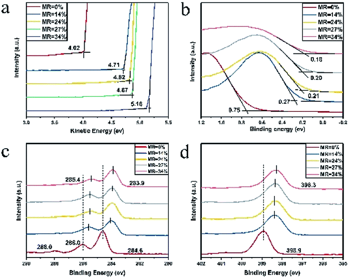
In order to elucidate the doping effect, the UV-vis-NIR, XPS and UPS were employed for further characterization of the multilayer CuPc/CN6-CP thin films with different doping concentration. The characteristic peaks of CuPc in UV-vis-NIR absorption are 627 nm and 692 nm (Fig. S4†). They both shows blue shift with the increase of doing concentration, and under high doping concentration the peak at 627 nm shifts to 615 nm and the peak at 692 nm shift to 682 nm. This phenomenon is similar with I2 doped CuPc films.32 We suppose this may attribute to the electron transfer from CuPc to CN6-CP. However, formation of ion pairs or charge transfer complexes can't be uncovered,33,34 as no new peaks appeared in the range of 300 to 1200 nm. The UPS and XPS spectra of pristine and doped CuPc films with different doping concentration is shown in Fig. 5. The work function of pristine CuPc is 4.02 eV and it shifts constantly to higher kinetic energy with the increase of doping concentration (Fig. 5a). Fig. 5b shows the HOMO region of pristine and doped CuPc films. The onset of valence band edge is 0.75 eV below the Fermi level for the pristine CuPc films. A continuous shift to lower binding energy region with the increase of doping concentration can be observed, corresponding to the shift of Fermi level towards the valence band edge. This is consistent with the observed decrease of Seebeck coefficient value with the increase of carrier concentration. Fig. 5c and d shows the XPS spectra of pristine and doped CuPc films. As shown in Fig. 5c, the C1s spectrum of pristine CuPc film have three characteristic peaks. Their binding energy are 288.0 eV, 286.0 eV and 284.6 eV and they are associated with a π–π* satellite feature from the pyrrole carbon, pyrrole carbon linked to nitrogen, and the aromatic carbon of the benzene rings, respectively.35–37 The peak at 288.0 eV is weak and it nearly disappear after doping. The other two peaks both shift to lower binding energy with the increase of doping concentration. Under a CN6-CP/CuPc MR value of 34% (TD = 0.5 nm), the two peaks shift from 284.6 eV to 283.9 eV and from 286.0 eV to 285.4 eV respectively. Similarly, as shown in Fig. 5d, the N1s spectrum of pristine CuPc film has a characteristic peak at 398.9 eV and it shifts to lower binding energy with the increasing of doping concentration. Under a MR value of 34% (TD = 0.5 nm), the peak shifts from 398.9 eV to 398.3 eV. Both the variation of C1s and N1s XPS spectra indicate the p-type doping induced by electron transfer from CuPc to CN6-CP. The data show that CN6-CP is an effective dopant for CuPc.
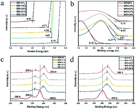 |
| | Fig. 5 The UPS and XPS of pristine and doped CuPc films. (a) The shift of work function, (b) the shift of HOMO level, the shift of binding energy of C 1s (c) and N 1s (d). | |
The microstructure of thin films
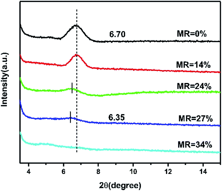
For investing the impact of doping on the morphology and microstructure ordering of CuPc films, AFM and XRD characterization are performed. The AFM morphology images of CuPc films with different doping concentration show that the grain size decrease with the increase of doping concentration, which illustrate the present of dopant layers destroy the crystallinity of pristine CuPc thin films (Fig. S6†). As shown in Fig. 6, only characteristic diffraction patterns of CuPc corresponding the present of α-phase CuPc microcrystal can be observed.38 No diffraction peaks of CN6-CP can be observed, showing that the total amorphous nature of CN6-CP in the thin film. The intensity of CuPc (200) peak at 2θ ∼ 6.5° shows a negative correlation to the doping concentration, that is in accordance with the results of AFM, which indicates that the introducing of CN6-CP layers has a detrimental effect on the crystallinity of CuPc film. In addition, the (200) peak shifts from 6.70° to 6.35° with the MR increase from 0 to 27% (TD = 0.3 nm), which indicates the interplanar spacing increase with the increase of doping concentration. This result is due to the intermolecular interactions between the CuPc molecules changes after the molecules are partially charged. The AFM images and XRD patterns illustrate the introduction of CN6-CP layers in between the CuPc layers will destroy the morphology and stacking ordering of CuPc films. And this effect is more significant under higher MR concentration.30,39–41 This phenomenon will hinder the improvement of charge transport performance, which may be solved by employing of a dopant molecule preferring a highly crystalline state in thin films.
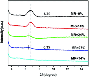 |
| | Fig. 6 The XRD measurements of pristine and doped CuPc films with different doping concentration deposited on OTS-modified substrate. | |
Conclusions
We use CN6-CP as dopant for the CuPc thin films to improve their thermoelectric performance. Through constructing multilayer devices and modification of the substrate surface, adjusting the thickness of films and doping concentration, the conductivity has been improved remarkably and it can reach up to 0.76 S cm−1. Meanwhile, the optimal power factor value is obtained as 1.3 μW m−1 K−2 when CN6-CP/CuPc molecular ratio of the film is 30% and Seebeck coefficient displays 130 μV K−1. Under the optimized condition, the carrier concentration of CuPc films is 2.8 × 1020 cm−3, which means that about 16% of CuPc molecules have been charged and CN6-CP is a very effective dopant for CuPc. Moreover, we demonstrated that alternatively deposited multilayer structure of small molecular semiconductor and dopant molecules offers a general strategy for investigation and optimization of their TE performance, as it is feasible for achieving high crystallinity and carrier concentration simultaneously. This is especial the case for those highly crystalline materials with poor solubility.
Conflicts of interest
There are no conflicts to declare.
Acknowledgements
We gratefully acknowledge the financial support from the National Key R&D Program of China (Grant No. 2017YFA0204701), the Chinese Academy of Sciences (Strategic Priority Research Program No. XDB12000000, QYZDY-SSW-SLH024) and National Natural Science Foundation of China (21333011, 21372227, 21661132006).
Notes and references
- Y. Sun, P. Sheng, C. Di, F. Jiao, W. Xu, D. Qiu and D. Zhu, Adv. Mater., 2012, 24, 932–937 CrossRef CAS.
- G. H. Kim, L. Shao, K. Zhang and K. P. Pipe, Nat. Mater., 2013, 12, 719–723 CrossRef CAS.
- Q. Zhang, Y. Sun, W. Xu and D. Zhu, Adv. Mater., 2014, 26, 6829–6851 CrossRef CAS.
- Y. Sun, W. Xu, C.-a. Di and D. Zhu, Synth. Met., 2017, 225, 22–30 CrossRef CAS.
- K. Harada, M. Sumino, C. Adachi, S. Tanaka and K. Miyazaki, Appl. Phys. Lett., 2010, 96, 253304 CrossRef.
- X. Huang, P. Sheng, Z. Tu, F. Zhang, J. Wang, H. Geng, Y. Zou, C. A. Di, Y. Yi, Y. Sun, W. Xu and D. Zhu, Nat. Commun., 2015, 6, 7408–7415 CrossRef CAS.
- D. Yuan, D. Huang, C. Zhang, Y. Zou, C. A. Di, X. Zhu and D. Zhu, ACS Appl. Mater. Interfaces, 2017, 9, 28795–28801 CrossRef CAS.
- T. Inabe and H. Tajima, Chem. Rev., 2004, 104, 5503–5533 CrossRef CAS.
- W. Chen, S. Chen, S. Chen, Y. Li Huang, H. Huang, D. C. Qi, X. Y. Gao, J. Ma and A. T. S. Wee, J. Appl. Phys., 2009, 106, 064910 CrossRef.
- S. Chakrabarti, S. Dey and A. J. Pal, Appl. Phys. Lett., 2011, 99, 053308 CrossRef.
- D. E. C. Yu, M. Matsuda, H. Tajima, T. Naito and T. Inabe, Dalton Trans., 2011, 40, 2283–2288 RSC.
- C. Hamann and I. Storbeck, Naturwissenschaften, 1963, 50, 327 CrossRef CAS.
- G. H. Heilmeier and S. E. Harrison, Phys. Rev., 1963, 132, 2010–2016 CrossRef CAS.
- L. Li, Q. Tang, H. Li, X. Yang, W. Hu, Y. Song, Z. Shuai, W. Xu, Y. Liu and D. Zhu, Adv. Mater., 2007, 19, 2613–2617 CrossRef CAS.
- J. Chen, D. Wang and Z. Shuai, J. Chem. Theory Comput., 2012, 8, 3338–3347 CrossRef CAS.
- D. Wang, W. Shi, J. Chen, J. Xi and Z. Shuai, Phys. Chem. Chem. Phys., 2012, 14, 16505–16520 RSC.
- T. Fukunaga, J. Am. Chem. Soc., 1976, 98, 610–611 CrossRef CAS.
- T. Fukunaga, M. D. Gordon and P. J. Krusic, J. Am. Chem. Soc., 1976, 98, 611–613 CrossRef CAS.
- Y. Karpov, T. Erdmann, I. Raguzin, M. Al-Hussein, M. Binner, U. Lappan, M. Stamm, K. L. Gerasimov, T. Beryozkina, V. Bakulev, D. V. Anokhin, D. A. Ivanov, F. Guenther, S. Gemming, G. Seifert, B. Voit, R. Di Pietro and A. Kiriy, Adv. Mater., 2016, 28, 6003–6010 CrossRef CAS.
- E. C. M. Chen and W. E. Wentworth, Chem. Phys., 1975, 63, 3183–3191 CAS.
- Y. Habibi, Chem. Soc. Rev., 2014, 43, 1519–1542 RSC.
- K. Bazaka, M. V. Jacob, W. Chrzanowski and K. Ostrikov, RSC Adv., 2015, 5, 48739–48759 RSC.
- M. Devynck, P. Tardy, G. Wantz, Y. Nicolas and L. Hirsch, Eur. Phys. J.: Appl. Phys., 2011, 56, 34106 CrossRef.
- N. Yoshino, Y. Yamamoto, K. Hamano and T. Kawase, Bull. Chem. Soc. Jpn., 1993, 66, 1754–1758 CrossRef CAS.
- H. Klauk, U. Zschieschang, J. Pflaum and M. Halik, Nature, 2007, 445, 745–748 CrossRef CAS.
- M. Maccarini, M. Himmelhaus, S. Stoycheva and M. Grunze, Appl. Surf. Sci., 2005, 252, 1941–1946 CrossRef CAS.
- D. Ji, X. Xu, L. Jiang, S. Amirjalayer, L. Jiang, Y. Zhen, Y. Zou, Y. Yao, H. Dong, J. Yu, H. Fuchs and W. Hu, J. Am. Chem. Soc., 2017, 139, 2734–2740 CrossRef CAS.
- Y. Guo, G. Yu and Y. Liu, Adv. Mater., 2010, 22, 4427–4447 CrossRef CAS.
- P. Pingel and D. Neher, Phys. Rev. B: Condens. Matter Mater. Phys., 2013, 87, 115209 CrossRef.
- B. Maennig, M. Pfeiffer, A. Nollau, X. Zhou, K. Leo and P. Simon, Phys. Rev. B: Condens. Matter Mater. Phys., 2001, 64, 195208 CrossRef.
- C. J. Brown, J. Chem. Soc. A, 1968, 2488–2493 RSC.
- Y. Yamamoto, K. Yoshino and Y. Inuishi, J. Phys. Soc. Jpn., 1979, 47, 1887–1891 CrossRef CAS.
- I. Salzmann, G. Heimel, M. Oehzelt, S. Winkler and N. Koch, Acc. Chem. Res., 2016, 49, 370–378 CrossRef CAS PubMed.
- I. E. Jacobs and A. J. Moule, Adv. Mater., 2017, 29, 1703063–1703101 CrossRef.
- J. X. Tang, C. S. Lee and S. T. Lee, Appl. Surf. Sci., 2006, 252, 3948–3952 CrossRef CAS.
- J. Y. Oh, W. S. Jang, T. I. Lee, J.-M. Myoung and H. K. Baik, Appl. Phys. Lett., 2011, 98, 023303 CrossRef.
- H. X. Wei, J. Li, Y. Cai, Z. Q. Xu, S. T. Lee, Y. Q. Li and J. X. Tang, Org. Electron., 2011, 12, 1422–1428 CrossRef CAS.
- S. I. Shihub and R. D. Gould, Thin Solid Films, 1996, 290, 390–394 CrossRef.
- K. Kang, S. Watanabe, K. Broch, A. Sepe, A. Brown, I. Nasrallah, M. Nikolka, Z. Fei, M. Heeney, D. Matsumoto, K. Marumoto, H. Tanaka, S. Kuroda and H. Sirringhaus, Nat. Mater., 2016, 15, 896–902 CrossRef CAS.
- J. Gao, E. T. Niles and J. K. Grey, J. Phys. Chem. Lett., 2013, 4, 2953–2957 CrossRef CAS.
- H. Kleemann, C. Schuenemann, A. A. Zakhidov, M. Riede, B. Lussem and K. Leo, Org. Electron., 2012, 13, 58–65 CrossRef CAS.
Footnote |
| † Electronic supplementary information (ESI) available. See DOI: 10.1039/c9ra06381a |
|
| This journal is © The Royal Society of Chemistry 2019 |
Click here to see how this site uses Cookies. View our privacy policy here. 
 Open Access Article
 This Open Access Article is licensed under a Creative Commons Attribution-Non Commercial 3.0 Unported Licence
 *ab and
Daoben
Zhu
*ab and
Daoben
Zhu