
 Open Access Article
 This Open Access Article is licensed under a Creative Commons Attribution-Non Commercial 3.0 Unported Licence
Barrier thickness dependence of MgxZn1−xO/ZnO quantum well (QW) on the performance of a p-NiO/QW/n-ZnO photodiode
Jun Dar Hwang * and
Jhong Yung Jiang
* and
Jhong Yung Jiang
Department of Electrophysics, National Chiayi University, No. 300 Syuefu Rd., Chiayi City 60004, Taiwan. E-mail: jundar@mail.ncyu.edu.tw
First published on 23rd September 2019
Abstract
An MgxZn1−xO/ZnO quantum well (QW) structure, with various barrier (MgxZn1−xO layer) thicknesses, was inserted into p-NiO/n-ZnO heterojunction photodiodes (HPDs) by using a radio-frequency magnetron sputtering system. The effect of various barrier thicknesses on the performance of QW-PDs was investigated. A band diagram shows that the QW-PD with 10 nm barrier layer presents a tunneling carrier transport mechanism, the UV- and visible-generated carriers tunnel through the thin barrier layer. Whereas the QW-PDs with thicker (≧25 nm) barrier layers show recombination-tunneling carrier transport. The visible-generated carriers are effectively confined within the well layer in the QW structure, causing the visible-response to be greatly reduced by more than 3 orders compared to that in the QW-PD with a 10 nm barrier layer. However, on further increasing the barrier thickness beyond 25 nm, the visible-response will no longer be reduced. In contrast, with decreasing the barrier thickness from 60 to 25 nm, the UV-response increases due to the overlap increase of the fundamental electron and hole wave function in the quantum well. Such a result drastically enhances the rejection ratio (320 nm/500 nm) from 264 for QW-PDs with a 10 nm barrier to 2986 for QW-PDs with a 25 nm barrier layer by a 11.3 ratio.
Introduction
ZnO-based materials are attractive semiconductors for fabricating ultraviolet (UV) photodetectors, such as p–n, Schottky-barrier, and metal–semiconductor–metal structures,1–12 due to the advantages of wide band gap (3.2 eV), high transparency (>80%) in the visible wavelength region, high exciton binding energy (60 meV), and non-toxicity.13,14 The addition of a Mg atom in ZnO leads to the formation of MgxZn1−xO with a band gap tuneable from 3.2 to 7.8 eV.1,15 However, the deep acceptor levels, low dopant solubility, and self-compensation in ZnO result in a reproducible and reliable p-type ZnO being not available.16 As a replacement for p-ZnO, p-NiO has been employed to fabricate p-NiO/n-ZnO heterojunction optoelectronics devices.17–25 NiO is an important p-type material with a direct wide band-gap of 3.0–4.0 eV and has merits of low-cost, earth advanced, and environmental friendliness for advanced photoelectric device applications.26–28 In spite of the developments in p-NiO/n-ZnO optoelectronic devices, many imperfections, such as oxygen vacancies in ZnO29,30 and nickel interstitials in NiO,22–31 are present at the NiO/ZnO heterojunction interface. These imperfections introduce large leakage current and visible response,32 which lower rectification29 and UV/visible rejection ratio in the p-NiO/n-ZnO heterojunction photodiodes (HPDs).32,33Quantum well (QW) structures have been applied in InxGa1−xN/GaN and AlxGa1−xN/GaN photodetectors to lower leakage current and enhance UV/visible rejection ratio, because the carriers generated by low-energy photons are confined in the QW.34,35 The barrier layer thickness in QW affect the exciton localization and piezoelectric field in the well, as well as the carrier transport and distribution in active layer.36 Such issues play a crucial role in determining the structure and optical qualities of QW. Effect of different barrier layer thickness on the InxGa1−xN/GaN QW opto-electronic devices were studied, including light-emitting diodes, solar cells and photodetectors.37–41 Previously, most MgxZn1−xO/ZnO QW were studied in optical and structural properties.42–52 MgxZn1−xO/ZnO QW was employed to investigate light-polarization53 and light-emitting diodes.54,55 The application of MgxZn1−xO/ZnO QW in photodetector is less to our knowledge. For a QW design, it is desirable to have a thinner barrier thickness. Because for a given total QW thickness, a thinner barrier leads to higher absorption due to more wells. However a thinner barrier cannot effectively confine the generated electrons and holes in the well layer, which causes a large leakage current and visible response in UV photodetectors. It is therefore useful to seek a critical barrier thickness, while maintaining a low leakage current and achieving high performance in photodetectors.
In this work, an MgxZn1−xO/ZnO QW structure with various barrier thickness was inserted into p-NiO/n-ZnO HPDs using a low-cost radio-frequency (RF) magnetron sputtering system. The effect of various barrier layer (MgxZn1−xO) thickness on the performance of p-NiO/QW/n-ZnO QW-PDs was studied in detail.
Experimental
After cleaning, the ITO/glass substrates were loaded into RF-magnetron sputtering system to deposit a 300 nm-thick ZnO layer. Next, MgxZn1−xO/ZnO/MgxZn1−xO QW structured layers were consecutively deposited onto the ZnO layer using the same system.56 The barrier layer thickness of MgxZn1−xO varies from 10, 25, 40, to 60 nm, while the well layer thickness of ZnO keeps at 4 nm. Finally, the p-NiO with a thickness of 80 nm was deposited using the same RF sputtering system as a hole transport layer.25 The p-NiO/QW/n-ZnO QW-PDs were fabricated by evaporating Ni electrode with a interdigitated pattern onto the NiO surface. A schematic diagram of the prepared QW-PDs is shown in Fig. 1. The QW-PDs with barrier thickness of 10, 25, 40, and 60 nm are denoted as PD_A, PD_B, PD_C, and PD_D, respectively. The current–voltage (I–V) characteristic and photoresponse were measured using a Keithley 2400 source meter and a 300 W Xe arc lamp with monochromator. | ||
| Fig. 1 Schematic diagram of the prepared QW-PD. | ||
Results and discussion
The Mg content of the MgxZn1−xO film was measured by X-ray photoelectron spectroscopy and the film composition was determined to be Mg0.3Zn0.7O.11 The absorption measurement showed the bandgap of Mg0.3Zn0.7O, ZnO and NiO films to be 3.7, 3.25, and 3.15 eV, respectively.11,57 Fig. 2 shows the spectral responsivity as a function of the illumination wavelengths for the fabricated QW-PDs at a 2 V reverse-bias voltage. From the figure, a significant difference occurs between PD_A and the other QW-PDs; that is, the PD_A (with 10 nm-thick barrier layer) exhibits a higher responsivity than the other QW-PDs (PD_B ∼ PD_D). The PD_B, PD_C, and PD_D have similar responsivity for various wavelengths. This suggests that the PD_B, PD_C, and PD_D are subject to the same carrier transport mechanism, and differ from that of PD_A. The photogenerated carriers are easy to tunnel the thin (10 nm) barrier layer in PD_A and hence a higher responsivities. The PDs without a QW (w/o QW) structure is also illustrated in Fig. 2 for comparison. The PDs without a QW demonstrates a similar responsivity to PD_A for the wavelengths longer than 400 nm due to the thin barrier layer in PD_A. The PDs without a QW reveals only an absorption band for the wavelengths less than 400 nm, attributing to the absorption of ZnO. However the PDs with QW exhibits another sharply rising responsivity for the wavelengths smaller than 350 nm because the absorption of MgZnO layer. The blue shift of absorption wavelength in MgZnO, compared to that of ZnO, is a result of the introduction of Mg atom.11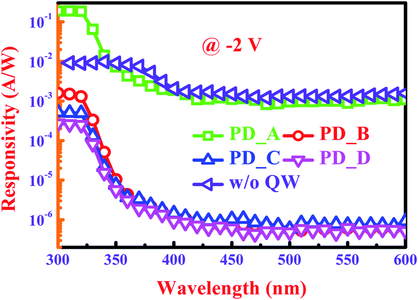 | ||
| Fig. 2 Spectral responsivity as a function of illumination wavelengths for the fabricated QW-PDs biased at 2 V reverse-bias voltage. | ||
Fig. 3 shows the responsivity versus various reverse-bias voltages responding to the incident wavelengths of 320 and 500 nm. With increasing reverse-bias voltage, the responsivities of all QW-PDs increase. Both the responsivities (320 and 500 nm) of PD_A demonstrate a high dependence on the bias-voltages; however a less dependence is observed in the PD_B ∼ PD_D. The result reveals that the photogenerated carriers tunnel through the thin barrier layer in PD_A; in contrast, the photogenerated carriers are confined within the well layer in PD_B ∼ PD_D. Compared to the visible response of the PD_A (5.5 × 10⁻³ A W−1), the visible response of PD_B is drastically reduced to 9.3 × 10⁻⁷ A W−1 by about 4 orders at 4 V reverse-bias voltage. This is consistent with previous experiments in which the current is carried by inter-well tunnelling in a QW-PD with 10 nm barrier layer, while the inter-well tunnelling is nearly negligible for the barrier layer larger than 20 nm.37 It was reported that the thicker barrier layer can suppress leakage current; however further increasing the barrier thickness beyond a certain value, the leakage current and visible-response will no longer be reduced.58 This leads to the PD_B, PD_C, and PD_D exhibit almost the same visible response, shown in Fig. 3. In contrast, the UV (320 nm) response is separated in the PD_B, PD_C, and PD_D. With decreasing the barrier thickness of QW-PDs from 60 nm to 25 nm, the UV response increases. For a thick barrier layer (60 nm), the UV response of PD_D is 4.7 × 10⁻⁴ A W−1 and it is raised to 2.8 × 10⁻³ A W−1 for the 25 nm barrier layer (PD_B) at 4 V reverse-bias voltage. Also from the figure, the PD_B, PD_C, and PD_D appear the same slopes in responsivity versus bias-voltage, and the slope is sharply different from that of the PD_A. Such a result again evidences the PD_B, PD_C, and PD_D exhibit the same carrier transport mechanism, and differ from that of PD_A.
 | ||
| Fig. 3 Responsivity versus various reverse-bias voltages responding to incident wavelength of 320 and 500 nm. | ||
The rejection ratio is defined as the responsivity at 320 nm divided by that at 500 nm. Fig. 4 shows the rejection ratio for the QW-PDs at a 4 V reverse-bias voltage. Clearly, the PD_B, PD_C, and PD_D presents a larger rejection ratio than the PD_A. The PD_B (25 nm barrier layer) exhibits the largest rejection ratio. The rejection ratio is largely enhanced from 264 to 3070 for the PD_A and PD_B, respectively, by a 11.6 times higher. This means that a suitable thickness barrier layer can greatly reduce the visible response and increase the rejection ratio. From Fig. 4, the PDs without a QW presents the lowest rejection ratio than those with QW. It means the insertion of QW strongly reduces the visible response and hence the QW-PDs exhibits a higher noise rejection ability than the PDs without QW. In order to study the different carrier transport mechanism between the QW-PDs with thin (10 nm) and thick (≧25 nm) barrier layers. The dark I–V characteristics for the PD_A (with 10 nm barrier layer) and PD_B (with 25 nm barrier layer) are shown in Fig. 5. A rather leaky I–V behaviour is observed in the PD_A, while the PD_B exhibits a good rectifying characteristic. It is well known that the leakage current (reverse-bias) is originated form thermally generated carriers. The thermally generated carriers can tunnel through the thin (10 nm) barrier layer, but are effectively confined within the well layer by the thick (≧25 nm) barrier in the MgxZn1−xO/ZnO QW structure.59 The inset of Fig. 5 shows the ln(I) versus ln(V) plot for the PD_A and PD_B, biased at forward voltage. For the entire voltage range, the current of the PD_A exhibits a linear dependence on bias-voltage, indicating that the carrier transport is dominated by tunnelling.60–62 However, there are two distinct regimes in the PD_B. At low forward voltages (V ≦ 0.7 V), referred to as regime I, the current increases exponentially, according to the relation I ∼ exp(αV), where α is a constant. The current transport shows a recombination-tunnelling mechanism, which is usually observed in wide band gap p–n diodes.63,64 At higher forward voltages (V ≧ 0.7 V), referred to as regime II, the I–V characteristic follows a power law (I ∼ Vm), which is generally attributed to a space-charge-limited current (SCLC) conduction. The m value is estimated to be 2.6. The high value of m (≧2), indicates SCLC conduction with exponential trap distribution.62
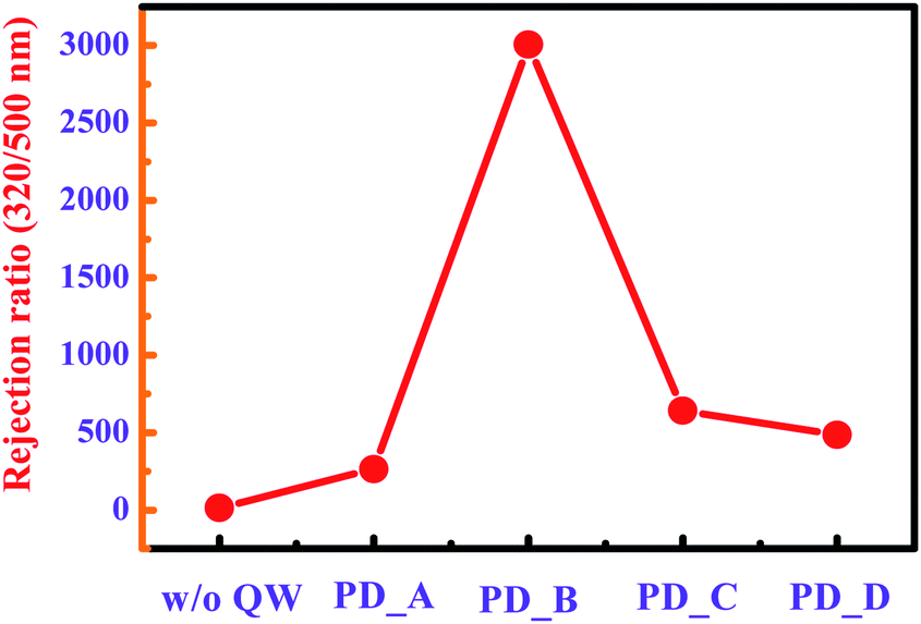 | ||
| Fig. 4 Rejection ratio for the all QW-PDs biased at 4 V reverse-bias voltage. | ||
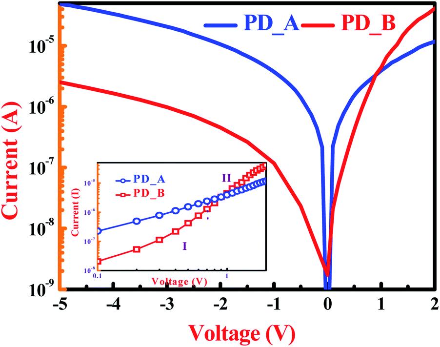 | ||
| Fig. 5 Dark I–V characteristics for the PD_A and PD_B. The inset is ln(I) versus ln(V) for PD_A and PD_B, biased at forward-voltage. | ||
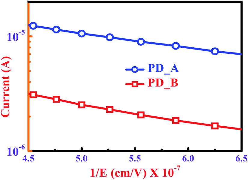
We also investigated the reverse-bias voltage regime, at which QW-PDs are normally operated. In this regime, the ln(I) is plotted as a function of the reciprocal of the electrical field E, as shown in Fig. 6. Both PD_A and PD_B present a good linear dependence of ln(I) on 1/E, which is described well by a trap-assisted tunnelling (TAT) mechanism.39,65 The trap-assisted tunnelling current JTAT is expressed as:

 | ||
| Fig. 6 ln(I) as a function of the reciprocal of the electrical field E for PD_A and PD_B, biased at reverse-voltage. | ||
Therefore, the tunnelling mechanism in the PD_A is attributed to the thinness of the barrier layer (10 nm) rather than the quality of the QW.
Based on above investigations, the band diagrams of the QW-PDs with thin (10 nm) and thick (≧25 nm) barrier layers, biased at reverse-voltage, are shown in Fig. 7(a) and (b), respectively, to elucidate the different carrier transport mechanisms. In Fig. 7(a), the visible light incident on the QW-PDs with 10 nm barrier layer is absorbed by the band-gap defects of MgZnO (denoted as process 1) and ZnO (denoted as process 2), however the UV light is absorbed by a band-to-band mechanism (denoted as process 3). Both photo-generated carriers tunnel through the thin barrier layer (10 nm), leading to higher visible and UV responses compared to the QW-PDs with thicker (≧25 nm) barrier layer. The band diagram (Fig. 7(b)) illustrates that, as the barrier thickness increases to 25 nm or more, the carriers generated from the visible light from MgZnO (denoted as process 4) and ZnO (denoted as process 5) are effectively confined within the well layer in the MgxZn1−xO/ZnO QW structure, which reduces the visible response by more than 3 orders compared to the QW-PD with the 10 nm barrier layer. Increasing the barrier thickness beyond a certain value (25 nm) will no longer reduce the visible response, causing the QW-PDs with thicker (≧25 nm) barrier layer to have similar visible responses, as shown in Fig. 3. In contrast, some of the carriers generated from UV light tunnel through the barrier by trap assistance (denoted as process 6) due to the carriers having higher energy than those generated by visible light. When decreasing the barrier thickness of the QW-PDs from 60 to 25 nm, the overlap of the fundamental electron and hole wave function in the quantum well increase and the carriers extraction by the trap-assisted tunnelling is enhanced.40,41,68 The issue leads to the enhancement of UV response with decreasing barrier thickness from 60 to 25 nm, as shown in Fig. 3.
 | ||
| Fig. 7 Band diagrams of QW-PDs with (a) thinner (10 nm) and (b) thicker (≧25 nm) barrier layers, biased at reverse-voltage. | ||
Conclusions
An MgxZn1−xO/ZnO QW structure, with various barrier (MgxZn1−xO layer) thickness, was inserted into p-NiO/n-ZnO HPDs using a low-cost RF magnetron sputtering system. The effect of the various barrier thickness on the performances of p-NiO/QW/n-ZnO QW-PDs were investigated. The QW-PDs with 10 nm-thick barrier layer presents higher UV and visible responses due to the photo-generated carriers tunnelling through the thin barrier layer. However, in the QW-PDs with thicker (≧25 nm) barrier layer, the carriers generated by visible light are effectively confined within the well layer in the QW structure, causing the visible response to be reduced by more than 3 orders compared to that in the QW-PD with 10 nm barrier layer. By increasing the barrier thickness beyond 25 nm, the visible response will no longer be reduced. In contrast, by decreasing the barrier thickness from 60 to 25 nm, the UV response increases due to the larger overlap of fundamental electron and hole wave function in the quantum well. As a result, the rejection ratio is drastically enhanced from 264 for QW-PDs with 10 nm barrier to 2986 for QW-PDs with 25 nm barrier layer (11.3-fold increase). Based on above investigations, a suitable thickness barrier layer can greatly reduce the visible response and increase the rejection ratio in the p-NiO/QW/n-ZnO HPDs.Conflicts of interest
There are no conflicts to declare.Acknowledgements
This work was supported by the Ministry of Science and Technology of the Republic of China, Taiwan, under Contract No. MOST 105-2112-M-415-001-MY3.References
- Y. F. Li, B. Yao, R. Deng, B. H. Li, J. Y. Zhang, Y. M. Zhao, D. Y. Jiang, Z. Z. Zhang, C. X. Shan, D. Z. Shen, X. W. Fan and Y. M. Lu, J. Phys. D: Appl. Phys., 2009, 42, 105102 CrossRef.
- C. T. Lee, T. S. Lin and C. H. Chen, J. Electron. Mater., 2015, 44, 4722–4725 CrossRef CAS.
- J. D. Hwang, D. H. Wu and S. B. Hwang, IEEE Photonics Technol. Lett., 2014, 26, 1081–1084 CAS.
- L. Su, Y. Zhu, X. Xu, H. Chen, Z. Tang and X. Fang, J. Mater. Chem. C, 2018, 6, 7776–7782 RSC.
- G. Cheng, X. Wu, B. Liu, B. Li, X. Zhang and Z. Du, Appl. Phys. Lett., 2011, 99, 203105 CrossRef.
- Y. Z. Li, X. M. Li and X. D. Gao, J. Alloys Compd., 2011, 509, 7193–7197 CrossRef CAS.
- H. Zhou, G. Fang, N. Liu and X. Zhao, Nanoscale Res. Lett., 2011, 6, 147 CrossRef PubMed.
- H. Y. Chen, K. W. Liu, X. Chen, Z. Z. Zhang, M. M. Fan, M. M. Jiang, X. H. Xie, H. F. Zhao and D. Z. Shen, J. Mater. Chem. C, 2014, 2, 9689–9694 RSC.
- S. H. Lee, S. H. Lim and J. S. Yu, Nanoscale Res. Lett., 2016, 11, 333 CrossRef PubMed.
- R. Liu, D. Jiang, Q. Duan, L. Sun, C. Tian, Q. Liang, S. Gao and J. Qin, Appl. Phys. Lett., 2014, 105, 043505 CrossRef.
- J. D. Hwang and G. S. Lin, Nanotechnology, 2016, 27, 375502 CrossRef CAS PubMed.
- Z. G. Ju, C. X. Shan, D. Y. Jiang, J. Y. Zhang, B. Yao, D. X. Zhao, D. Z. Shen and X. W. Fan, Appl. Phys. Lett., 2008, 93, 173505 CrossRef.
- H. Zhu, C. X. Shan, L. K. Wang, J. Zheng, J. Y. Zhang, B. Yao and D. Z. Shen, J. Phys. Chem. C, 2010, 114, 7169–7172 CrossRef CAS.
- W. Yang, S. S. Hullavarad, B. Nagaraj, I. Takeuchi, R. P. Sharma, T. Venkatesan, R. D. Vispute and H. Shen, Appl. Phys. Lett., 2003, 82, 3424–3426 CrossRef CAS.
- Y. Zhu, H. Zhou, G. Fang and M. Li, Semicond. Sci. Technol., 2012, 27, 065003 CrossRef.
- S. Mridha and D. Basak, J. Appl. Phys., 2007, 101, 083102 CrossRef.
- J. M. Nel, F. D. Auret, L. Wu, M. J. Legodi, W. E. Meyer and M. Hayes, Sens. Actuators, B, 2004, 100, 270–276 CrossRef CAS.
- J. Y. Wang, C. Y. Lee, Y. T. Chen, C. T. Chen, Y. L. Chen, C. F. Lin and Y. F. Chen, Appl. Phys. Lett., 2009, 95, 131117 CrossRef.
- Y. Y. Xi, Y. F. Hsu, A. B. Djurišic, A. M. C. Ng, W. K. Chan, H. L. Tam and K. W. Cheah, Appl. Phys. Lett., 2008, 92, 113505 CrossRef.
- N. Park, K. Sun, Z. Sun, Y. Jiang and D. Wang, J. Mater. Chem. C, 2013, 1, 7333–7338 RSC.
- A. Echresh, C. O. Chey, M. Z. Shoushtari, V. Khrnovskyy, O. Nur and M. Willander, J. Alloys Compd., 2015, 632, 165–171 CrossRef CAS.
- R. Debnath, T. Xie, B. Wen, W. Li, J. Y. Ha, N. F. Sullivan, N. V. Nguyen and A. A. Motayed, RSC Adv., 2015, 5, 14646–14652 RSC.
- H. Ohta, M. Hirano, K. Nakahara, H. Maruta, T. Tanabe, M. Kamiya, T. Kamiya and H. Hosono, Appl. Phys. Lett., 2003, 83, 1029–1031 CrossRef CAS.
- Y. Vygranenko, K. Wang and A. Nathan, Appl. Phys. Lett., 2006, 89, 172105 CrossRef.
- J. D. Hwang and W. M. Lin, IEEE Trans. Nanotechnol., 2019, 18, 126–131 CAS.
- H. Imran, T. M. Abdolkader and N. Z. Butt, IEEE Trans. Electron Devices, 2016, 63, 3584–3590 CAS.
- M. Awais, M. Rahman, J. M. D. MacElroy, N. Coburn, D. Dini, J. G. Vos and D. P. Dowling, Surf. Coat. Technol., 2010, 204, 2729–2736 CrossRef CAS.
- A. G. Marrani, V. Novelli, S. Sheehan, D. P. Dowling and D. Dini, ACS Appl. Mater. Interfaces, 2014, 6, 143–152 CrossRef CAS PubMed.
- H. L. Mosbacker, Y. M. Strzhemechny, B. D. White, P. E. Smith, D. C. Look, D. C. Reynolds, C. W. Litton and L. J. Brillson, Appl. Phys. Lett., 2005, 87, 012102 CrossRef.
- R. E. Schifano, V. Monakhov, U. Grossner and B. G. Svensson, Appl. Phys. Lett., 2007, 91, 193507 CrossRef.
- M. R. Hasan, T. Xie, S. C. Barron, G. Liu, N. V. Nguyen, A. Motayed and M. V. Rao, APL Mater., 2015, 3, 106101 CrossRef PubMed.
- M. Patel, H. S. Kim and J. Kim, Adv. Electron. Mater., 2015, 1, 1500232 CrossRef.
- Y. R. Li, C. Y. Wan, C. T. Chang, W. L. Tsai, Y. C. Huang, K. Y. Wang and P. Y. Yang, Vacuum, 2015, 118, 48–54 CrossRef CAS.
- C. L. Yu, R. W. Chuang, S. J. Chang, P. C. Chang, K. H. Lee and J. C. Lin, IEEE Photonics Technol. Lett., 2007, 19, 846–848 CAS.
- S. K. Zhang, W. B. Wang, F. Yun, L. He, H. Morkoç, X. Zhou, M. Tamargo and R. R. Alfano, Appl. Phys. Lett., 2002, 81, 4628–4630 CrossRef CAS.
- M. M. Liang, G. E. Weng, J. Y. Zhang, X. M. Cai, X. Q. Lu, L. Y. Ying and B. P. Zhang, Chin. Phys. B, 2014, 23, 054211 CrossRef.
- S. K. H. Sim, H. C. Liu, A. Shen, M. Gao, K. F. Lee, M. Buchanan, Y. Ohno, H. Ohno and E. H. Li, Infrared Phys. Technol., 2001, 42, 115–121 CrossRef CAS.
- J. J. Wierer Jr, D. D. Koleske and S. R. Lee, Appl. Phys. Lett., 2012, 100, 111119 CrossRef.
- N. Watanabe, H. Yokoyama, N. Shigekawa, K. I. Sugita and A. Yamamoto, Jpn. J. Appl. Phys., 2012, 51, 10ND10 CrossRef.
- L. Redaelli, A. Mukhtarova, A. Ajay, A. Núñez-Cascajero, S. Valdueza-Felip, J. Bieuse, C. Durand, J. Eymery and E. Monroy, Jpn. J. Appl. Phys., 2015, 54, 072302 CrossRef.
- G. B. Lin, D. Y. Kim, Q. Shan, J. Cho, E. F. Schubert, H. Shim, C. Sone and J. K. Kim, IEEE Photonics J., 2013, 5, 1600207 Search PubMed.
- M. Stölzel, J. Kupper, M. Brandt, A. Müller, G. Benndorf, M. Loren and M. Grundmann, J. Appl. Phys., 2012, 111, 063701 CrossRef.
- H. R. Chen, C. Y. Tsai, Y. C. Huang, C. C. Kuo, H. C. Hsu and W. F. Hsieh, J. Phys. D: Appl. Phys., 2016, 49, 095105 CrossRef.
- T. Makino, C. H. Chia, N. T. Tuan, H. D. Sun, Y. Segawa, M. Kawasaki, A. Ohtomo, K. Tamura and H. Koinuma, Appl. Phys. Lett., 2000, 77, 975–977 CrossRef CAS.
- B. Laumer, F. Schuster, T. A. Wassner, M. Stutzmann, M. Rohnke, J. Schörmann and M. Eickhoff, J. Appl. Phys., 2012, 111, 113504 CrossRef.
- J. W. Sun, Y. M. Lu, Y. C. Liu, D. Shen, Z. Z. Zhang, B. H. Li, J. Y. Zhang, B. Yao, D. X. Zhao and X. W. Fan, J. Phys. D: Appl. Phys., 2007, 40, 6541–6544 CrossRef CAS.
- S. M. Li, B. J. Kwon, H. S. Kwack, L. H. Jin, Y. H. Cho, Y. S. Park, M. S. Han and M. S. Park, J. Appl. Phys., 2010, 107, 033513 CrossRef.
- T. Makino, N. T. Tuan, H. D. Sun, C. H. Chia, Y. Segawa, M. Kawasaki, A. Ohtomo, K. Tamura, T. Suemoto, H. Akiyama, M. Baba, S. Saito, T. Tomita and H. Koinuma, Appl. Phys. Lett., 2001, 78, 1979–1981 CrossRef CAS.
- M. Brandt, M. Lange, M. Stölzel, A. Müller, G. Benndorf, J. Zippel, J. Lenzner, M. Lorenz and M. Grundmann, Appl. Phys. Lett., 2010, 97, 052101 CrossRef.
- J. Zhu, A. Y. Kuznetsov, M. S. Han, Y. S. Park, H. K. Ahn, J. W. Ju and I. H. Lee, Appl. Phys. Lett., 2007, 90, 211909 CrossRef.
- S. C. Su, H. Zhu, L. X. Zhang, M. He, L. Z. Zhao, S. F. Yu, J. N. Wang and F. C. C. Ling, Appl. Phys. Lett., 2013, 103, 131104 CrossRef.
- J. Zippel, M. Stölzel, A. Müller, G. Benndorf, M. Loren, H. Hochmuth and M. Grundmann, Phys. Status Solidi B, 2010, 247, 398–404 CrossRef CAS.
- G. Tabares, A. Hierro, M. Lopez-Ponce, E. Muñoz, B. Vinter and J. M. Chauveau, Appl. Phys. Lett., 2015, 106, 061114 CrossRef.
- Y. S. Choi, J. W. Kang, B. H. Kim and S. J. Park, Opt. Express, 2013, 21, 31560–31566 CrossRef PubMed.
- X. Mo, G. Fang, H. Long, H. Huang, S. Li, H. Wang and P. Qin, Semicond. Sci. Technol., 2013, 28, 015016 CrossRef.
- J. D. Hwang, C. C. Yang and C. M. Chu, ACS Appl. Mater. Interfaces, 2017, 9, 23904–23908 CrossRef CAS PubMed.
- J. D. Hwang and T. H. Ho, Mater. Sci. Semicond. Process., 2017, 71, 396–400 CrossRef CAS.
- A. Teke, S. Dogan, F. Yun, M. A. Reshchikov, H. Le, X. Q. Liu, H. Morkoç, S. K. Hang, W. B. Wang and R. R. Alfano, Solid-State Electron., 2003, 47, 1401–1408 CrossRef CAS.
- Y. Irokawa, B. Luo, J. Kim, J. R. Larcche, F. Ren, K. H. Baik, S. J. Pearton, C. C. Pan, G. T. Chen, J. I. Chi, S. S. Park and Y. J. Park, Appl. Phys. Lett., 2003, 83, 2271–2273 CrossRef CAS.
- J. W. Kang, Y. S. Choi, B. H. Kim, C. G. Kang, B. H. Lee, C. W. Tu and S. J. Park, Appl. Phys. Lett., 2014, 104, 051120 CrossRef.
- N. K. Reddy, Q. Ahsanulhaq, J. H. Kim and Y. B. Hahn, Appl. Phys. Lett., 2008, 92, 043127 CrossRef.
- R. N. Gayen and S. R. Bjhattacharyya, J. Phys. D: Appl. Phys., 2016, 49, 115102 CrossRef.
- R. Ghosh and D. Basak, Appl. Phys. Lett., 2007, 90, 243106 CrossRef.
- J. D. Yeh, S. L. Gu, S. M. Zhu, W. Liu, S. M. Liu, R. Zhang, Y. Shi and Y. D. Zheng, Appl. Phys. Lett., 2006, 88, 182112 CrossRef.
- R. Mahapatra, A. K. Chakraborty, N. Poolamai, A. Horsfall, S. Chattopadhyay, N. G. Wright, K. S. Coleman, P. G. Coleman and C. P. Burrows, J. Vac. Sci. Technol., B: Microelectron. Nanometer Struct.--Process., Meas., Phenom., 2007, 25, 217–223 CrossRef CAS.
- H. Tanaka, S. Fujita and S. Fujita, Appl. Phys. Lett., 2005, 86, 192911 CrossRef.
- T. Makino, Y. Segawa, A. Tsukazaki, H. Saito, S. Takeyama, S. Akasaka, K. Nakahara and M. Kawasaki, Phys. Rev. B: Condens. Matter Mater. Phys., 2013, 87, 085312 CrossRef.
- J. Aippel, M. Stölel, A. Müller, G. Benndorf, M. Lorenz, H. Hochmuth and M. Grundmann, Phys. Status Solidi B, 2010, 247, 398–404 CrossRef.
| This journal is © The Royal Society of Chemistry 2019 |