
 Open Access Article
 This Open Access Article is licensed under a Creative Commons Attribution-Non Commercial 3.0 Unported Licence
Structures and characteristics of atomically thin ZrO2 from monolayer to bilayer and two-dimensional ZrO2–MoS2 heterojunction†
Junhui Weng and
Shang-Peng Gao *
*
Department of Materials Science, Fudan University, Shanghai 200433, P. R. China. E-mail: gaosp@fudan.edu.cn
First published on 16th October 2019
Abstract
The understanding of the structural stability and properties of dielectric materials at the ultrathin level is becoming increasingly important as the size of microelectronic devices decreases. The structures and properties of ultrathin ZrO2 (monolayer and bilayer) have been investigated by ab initio calculations. The calculation of enthalpies of formation and phonon dispersion demonstrates the stability of both monolayer and bilayer ZrO2 adopting a honeycomb-like structure similar to 1T-MoS2. Moreover, the 1T-ZrO2 monolayer or bilayer may be fabricated by the cleavage from the (111) facet of non-layered cubic ZrO2. Moreover, the contraction of in-plane lattice constants in monolayer and bilayer ZrO2 as compared to the corresponding slab in cubic ZrO2 is consistent with the reported experimental observation. The electronic band gaps calculated from the GW method show that both the monolayer and bilayer ZrO2 have large band gaps, reaching 7.51 and 6.82 eV, respectively, which are larger than those of all the bulk phases of ZrO2. The static dielectric constants of both monolayer ZrO2 (ε‖ = 33.34, ε⊥ = 5.58) and bilayer ZrO2 (ε‖ = 33.86, ε⊥ = 8.93) are larger than those of monolayer h-BN (ε‖ = 6.82, ε⊥ = 3.29) and a strong correlation between the out-of-plane dielectric constant and the layer thickness in ultrathin ZrO2 can be observed. Hence, 1T-ZrO2 is a promising candidate in 2D FETs and heterojunctions due to the high dielectric constant, good thermodynamic stability, and large band gap for applications. The interfacial properties and band edge offset of the ZrO2–MoS2 heterojunction are investigated herein, and we show that the electronic states near the VBM and CBM are dominated by the contributions from monolayer MoS2, and the interface with monolayer ZrO2 will significantly decrease the band gap of the monolayer MoS2.
Introduction
With the discovery of graphene, two-dimensional (2D) materials have attracted wide attention due to their excellent properties and many possible applications in the fields of electronic devices and catalysis.1–8 Among the applications of 2D materials in microelectronic devices, 2D field-effect transistors (FETs) have attracted tremendous attention due to their excellent electrical characteristics, such as ultra-low power consumption, high current switching ratio, and large carrier mobility.9–11 The semiconductor layers in 2D FETs are 2D semiconductor materials such as MoS2, WS2, and phosphorus.The dielectric materials commonly used as dielectric layers of 2D FETs include zirconium dioxide (ZrO2), hafnium oxide (HfO2), silicon dioxide (SiO2), and hexagonal layered boron nitride (h-BN).3,5,11,12 In general, the dielectric layer plays a key role in the performance of 2D FETs. The interfacial properties between the dielectric layer and the 2D semiconductor layer are critical to the performances of 2D FETs.13–15 The interfacial impurities and the scattering of remote phonons can seriously affect the carriers in the 2D semiconductor and cause a decrease in the device performance due to the atomic-scale characteristics of 2D semiconductor materials.14–17 Monolayer and few-layer h-BN possess excellent properties such as large band gaps (5.97 eV), good mechanical strength, surface charge traps and absence of dangling bonds, which make h-BN a popular dielectric substrate in 2D FETs.18–20 Moreover, adopting h-BN as the dielectric layer in 2D FETs can effectively shield scattering effects to increase the carrier mobility. Many previous reports have indicated that high-k materials with larger dielectric constant can effectively increase the carrier mobility of 2D semiconductors by reducing the scattering of Coulomb impurities.6,21,22 However, the dielectric constant of monolayer h-BN (ε‖ = 6.82, ε⊥ = 3.29) is not outstanding,23 particularly being only 3.29 along the out-of-plane direction, which may limit the performance of the device. Thus, it is desirable to find a dielectric material with fewer interfacial defects, high dielectric constant and a large band gap to improve the performances of 2D FETs.
To increase the gate capacitance and preserve high channel mobility through the dielectric screening effect, the integration of high-k technology with MoS2 transistors is essential.5 ZrO2 is widely used as a high-k dielectric material in the dielectric layer of FETs. Compared with h-BN, bulk ZrO2 has more surface defects and impurities on the surface, which greatly reduces the electrical properties of the device. It is well known that the bulk ZrO2 has three polymorphs at atmospheric pressure, which are cubic fluorite (Fm![[3 with combining macron]](https://www.rsc.org/images/entities/char_0033_0304.gif) m) from 2377 to 2710 °C, tetragonal (P42/nmc) from 1205 to 2377 °C and monoclinic structures (P21/c) at room temperature.24 With respect to the surface condition of these three polymorphs, the surface defects of the monoclinic phase and the tetragonal phase are much larger than those of the cubic phase and thus, the surface of the cubic phase prevents the decrease in electrical properties of the semiconductor. However, at ambient atmosphere, the cubic and tetragonal phases of pure ZrO2 are dynamically unstable, except for the monoclinic phase.25,26 It is worth noting that the stability properties of bulk and ultra-thin materials may be different. In addition, the thickness of the gate dielectric layer has a significant effect on the performance of the transistor. In order to reduce the gate voltage to achieve good switching behavior, a thinner gate dielectric layer is also required.27 Therefore, it is demanding to explore the stable structure and properties of ZrO2 at the ultrathin level (monolayer or few-layer).
m) from 2377 to 2710 °C, tetragonal (P42/nmc) from 1205 to 2377 °C and monoclinic structures (P21/c) at room temperature.24 With respect to the surface condition of these three polymorphs, the surface defects of the monoclinic phase and the tetragonal phase are much larger than those of the cubic phase and thus, the surface of the cubic phase prevents the decrease in electrical properties of the semiconductor. However, at ambient atmosphere, the cubic and tetragonal phases of pure ZrO2 are dynamically unstable, except for the monoclinic phase.25,26 It is worth noting that the stability properties of bulk and ultra-thin materials may be different. In addition, the thickness of the gate dielectric layer has a significant effect on the performance of the transistor. In order to reduce the gate voltage to achieve good switching behavior, a thinner gate dielectric layer is also required.27 Therefore, it is demanding to explore the stable structure and properties of ZrO2 at the ultrathin level (monolayer or few-layer).
For transition metal dichalcogenides (TMDs), there are mainly two different monolayer structures, one of which is the 2H structure with hexagonal honeycombs and the other is the 1T structure with centered honeycombs.28 In this paper, the stabilities of the 1T structures of monolayer and bilayer ZrO2, which are analogous to the 1T structure of TMDs, have been investigated. The phase stability and dynamical stability of monolayer and bilayer 1T-ZrO2 are revealed based on the calculations of the formation energy and phonon dispersion, respectively. The feasible methods of experimental preparation of monolayer and few-layer 1T-ZrO2 are also discussed. Next, the band structures and static dielectric constants of monolayer and bilayer ZrO2 are calculated, and the band gap values of 2D ZrO2 are predicted by the GW method in comparison with bulk ZrO2 polymorphs. Finally, we exhibit the interfacial properties of heterojunctions formed by 2D ZrO2/MoS2, including the effects of the monolayer 1T-ZrO2 dielectric layer on the electronic structure of monolayer MoS2 and electron transfer and redistribution on the interface of the ZrO2–MoS2 heterojunction.
Methods
All calculations except for the GW correction were implemented within the framework of the density functional theory (DFT) with a plane-wave basis by means of CASTEP in the Materials Studio 17.1.29 The interactions between the atomic core and the valence electrons were described by the on-the-fly generated (OTFG) norm-conserving pseudopotentials in the CASTEP code. The generalized gradient approximation (GGA) parametrized by the Perdew–Burke–Ernzerhof (PBE) functional was chosen for the exchange–correlation term, and the kinetic energy cut-off was set to 1200 eV for the plane-wave basis sets. The Brillouin zone was sampled by a Monkhorst-Pack grid of 15 × 15 × 1 in our calculations. The full geometry optimization of structures was implemented by the Broyden–Fletcher–Goldfarb–Shanno (BFGS) scheme.30 The total energy difference, the maximum Hellmann–Feynman forces acting on each atom, the maximum stress, and the maximum displacement change were below 5 × 10⁻⁶ eV per atom, 0.01 eV Å−1, 0.02 GPa, and 5 × 10⁻⁴ Å, respectively, as the convergence tolerance for the geometry optimization. An adequate vacuum layer (larger than 18 Å) along the c-direction was adopted to avoid the spurious interlayer interactions between periodic images. The van der Waals (vdW) correction with the semiempirical correction methods of the Grimme scheme31 was implemented for our calculations. Structural stability was determined by phonon calculations based on density functional perturbation theory (DFPT).32 The static dielectric constant (containing both the ionic and the electronic response) was calculated by the DFPT formalism of the electric field. In the calculation of the electronic properties in the 2D ZrO2–MoS2 heterojunction (a semiconducting 2H monolayer of MoS2 interfacing with a ZrO2 monolayer), the parameter settings of the exchange–correlation term, pseudopotentials, cutoff energy, and k-point sampling were consistent with the calculations of monolayer and bilayer ZrO2. Dipole correction was applied to the calculations of properties of the 2D ZrO2–MoS2 heterojunction. The band edge positions relative to the vacuum level were determined by averaging the electrostatic potential in the planes perpendicular to the normal of the slabs (monolayer and bilayer ZrO2, 2D ZrO2–MoS2 heterojunction).In order to give a more reliable band gap prediction for the few-layer ZrO2, the GW method was used to correct the band structures obtained from DFT-GGA, which has the well-known band gap underestimation phenomenon. GW calculations were performed using the standard one-shot G0W0 approach implemented in the ABINIT8.2.2 package.33 The Fritz-Haber-Institute (FHI) norm-conserving pseudopotential (Troullier–Martins scheme)34 was chosen. Monkhorst-Pack grids of 8 × 8 × 8, 8 × 8 × 6, 6 × 6 × 6, and 12 × 12 × 1 were used in the GW calculations for cubic, tetragonal, monoclinic, and 2D ZrO2 respectively. The screening in the GW calculation was treated with the plasmon-pole model. The polarization function was calculated within the random phase approximation. Coulomb interaction was truncated using a cutoff radius slightly smaller than half the periodic length along the perpendicular direction in the GW calculation of monolayer and bilayer ZrO2.
Results and discussion
Structures of monolayer and bilayer ZrO2
In this study, we have investigated the possible structures of monolayer and bilayer ZrO2 by optimizing various slabs cut from bulk ZrO2 polymorphs and by deriving similar structures of TMDs. We found that the 1T structure of monolayer and bilayer ZrO2, which is analogous to 1T-MoS2 and can be regarded as a cleavage slab from cubic ZrO2, is energetically favorable and dynamically stable (see the discussion in the next section). The monolayer and bilayer structures of 1T-ZrO2 are shown in Fig. 1a and b, respectively. For the monolayer structure of 1T-ZrO2, the two O atoms staggered with each other constitute an octahedral structure with Zr atoms (located in the center of the octahedron), forming the O–Zr–O trilayer slab, as shown in Fig. 1a. It can be regarded as a hexagonal layer of positively charged Zr atoms sandwiched between two hexagonal layers of negatively charged O atoms. For the bilayer structure of 1T-ZrO2, as shown in Fig. 1b, the bilayer structure is constituted of two monolayers of 1T-ZrO2, with each Zr atom of one monolayer forming an additional bond with the adjacent oxygen atom of the other monolayer.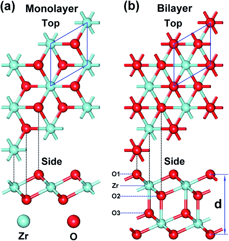 | ||
| Fig. 1 Top and side views of (a) the monolayer of 1T-ZrO2 and (b) the bilayer of 1T-ZrO2, the red and the powder blue spheres represent O atoms and Zr atoms, respectively. The blue rhombus frame denotes the primitive cell. | ||
The optimized lattice constants and Zr–O interatomic distances of 1T-ZrO2 (monolayer and bilayer) and cubic ZrO2 are shown in Table 1. The lattice constants of the monolayer and bilayer are 3.28 Å and 3.42 Å, respectively. We found that the lattice constant of the bilayer (3.42 Å) becomes larger as compared to that of the monolayer (3.28 Å). The Zr–O interatomic distance of the monolayer ZrO2 is 2.12 Å and all Zr–O bond lengths are equal, and are smaller than those in cubic ZrO2. However, for the bilayer, we found that the O–Zr bonds are of three different types, as indicated in the side view of the bilayer in Fig. 1b. The bond lengths of O1–Zr, O2–Zr, and O3–Zr are 2.17 Å, 2.14 Å, and 2.24 Å, respectively, where the O2–Zr bond length is the smallest and O3–Zr bond length is the largest. It is worth noting that the O3–Zr bond is the interlayer bond between two monolayers, which is a strong chemical bond that is different from the weak vdW interlayer interaction in graphite and TMDs.35,36 We further characterized the bonding properties of the Zr–O chemical bonds between the layers (i.e. ionic or covalent characters) through the electron density distribution and electron density difference of bilayer ZrO2.
The bulk ZrO2 has three crystal phases at atmospheric pressure, namely, cubic fluorite, tetragonal and monoclinic structures. With increasing temperature, the monoclinic crystal structure of ZrO2 reversibly transforms into cubic and tetragonal phases. Interestingly, we found that the monolayer and bilayer of 1T-ZrO2 can be cleaved from the (111) facet of the bulk ZrO2 (cubic phase), and the tri-layer slice of O–Zr–O atomic layers is shown in the blue dashed rectangle in Fig. 2a. The structure of the cleaved 2D slice is fully optimized and the relaxed structure is completely consistent with the 1T-ZrO2 monolayer, as shown in Fig. 2b. It is noticeable that in the process of geometric optimization of the cleaved 2D slice, the size of the Zr–O bond length was reduced from 2.20 Å to 2.12 Å, and the Zr–O–Zr bond angle was diminished from 109.47° to 101.02°. The total energy of the cleaved 2D slice was gradually reduced from −2188.36 eV to −2189.39 eV (corresponding to that of the monolayer 1T-ZrO2), with the energy difference of 1.03 eV. In a similar way, the bilayer of the cleaved slice was geometrically relaxed, and the relaxed structure was also consistent with that of the bilayer of 1T-ZrO2, as shown in Fig. 2c. The total energy of the bilayer of the cleaved slice was reduced from −4378.80 to −4379.28 eV (corresponding to that of the bilayer of 1T-ZrO2), and the energy difference is 0.48 eV (or 0.24 eV per formula unit), which is less than that of the monolayer (1.03 eV per formula unit). Overall, the in-plane lattice constants of the monolayer and bilayer (3.28 and 3.42 Å, respectively) have a contraction as compared to the corresponding slab in cubic ZrO2 (3.59 Å), which is consistent with the experimental results of the in-plane lattice constants for the ultrathin ZrO2 film grown on the Rh (111) substrate and the oxidized surface of Pt3Zr (0001) annealed in ultrahigh vacuum (UHV).37,38
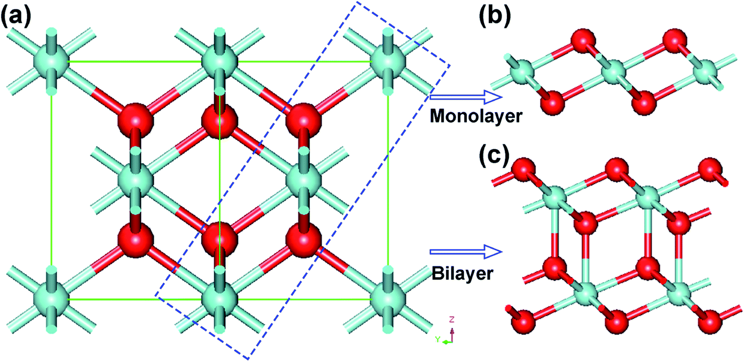 | ||
| Fig. 2 (a) The structure of bulk ZrO2 (cubic phase), and blue rectangular dashed frame denotes the cleavage of the cubic ZrO2 (111) facet. The relaxed structures of the cleaved monolayer and bilayer 2D slices are shown in (b) and (c), respectively. | ||
Stability of the monolayer and bilayer ZrO2
The enthalpy of formation was calculated to investigate the phase stability of 1T-ZrO2 (the monolayer and bilayer). The expression is as follows:| ΔHZrO2 = EZrO2 − EZr − EO2 | (1) |
Phonon calculations were performed to investigate the dynamical stability of the monolayer and bilayer ZrO2, and the phonon dispersions and phonon density of states (DOS) are shown in Fig. 3. There are no imaginary frequencies existing in the phonon dispersions of both the monolayer and bilayer ZrO2 as depicted in Fig. 3a and c, demonstrating that both the monolayer and bilayer ZrO2 are dynamically stable. Monolayer 1T-HfO2 is also dynamically stable as shown in our previous study.39 The phonon dispersion of the monolayer contains three acoustic branches and six optical branches, and the phonon dispersion of the bilayer possesses three acoustic branches and fifteen optical branches because the atoms in the unit cell double. In the vicinity of the Γ point, there are two acoustic branches vibrating in-plane, which are the longitudinal acoustic branch (LA) and the transverse acoustic branch (TA). The LA and TA are approximately linear dispersions near the Γ point and the slopes indicate the group velocities.40 From the phonon dispersion curves of the monolayer and bilayer, the sound velocity of the monolayer and bilayer can be acquired. For the TA and LA modes of the monolayer along the Γ–M high symmetrical line, the sound velocities at the long-wavelength limit are about 5550.9 and 8491.6 m s−1, respectively. Similarly, the sound velocities of the bilayer can be obtained as about 4259.3 and 6356.2 m s−1, respectively, which are smaller than those of the monolayer (5550.9 and 8491.6 m s−1) but very close to the MoS2 case of 4200 m s−1 (TA) and 6700 m s−1 (LA).41 In addition, we found that the out-of-plane transverse acoustic branch (ZA) in 2D systems approximates a parabolic curve near the Γ point, which is a typical mode of 2D materials consistent with the 2D structure of 1T-ZrO2.
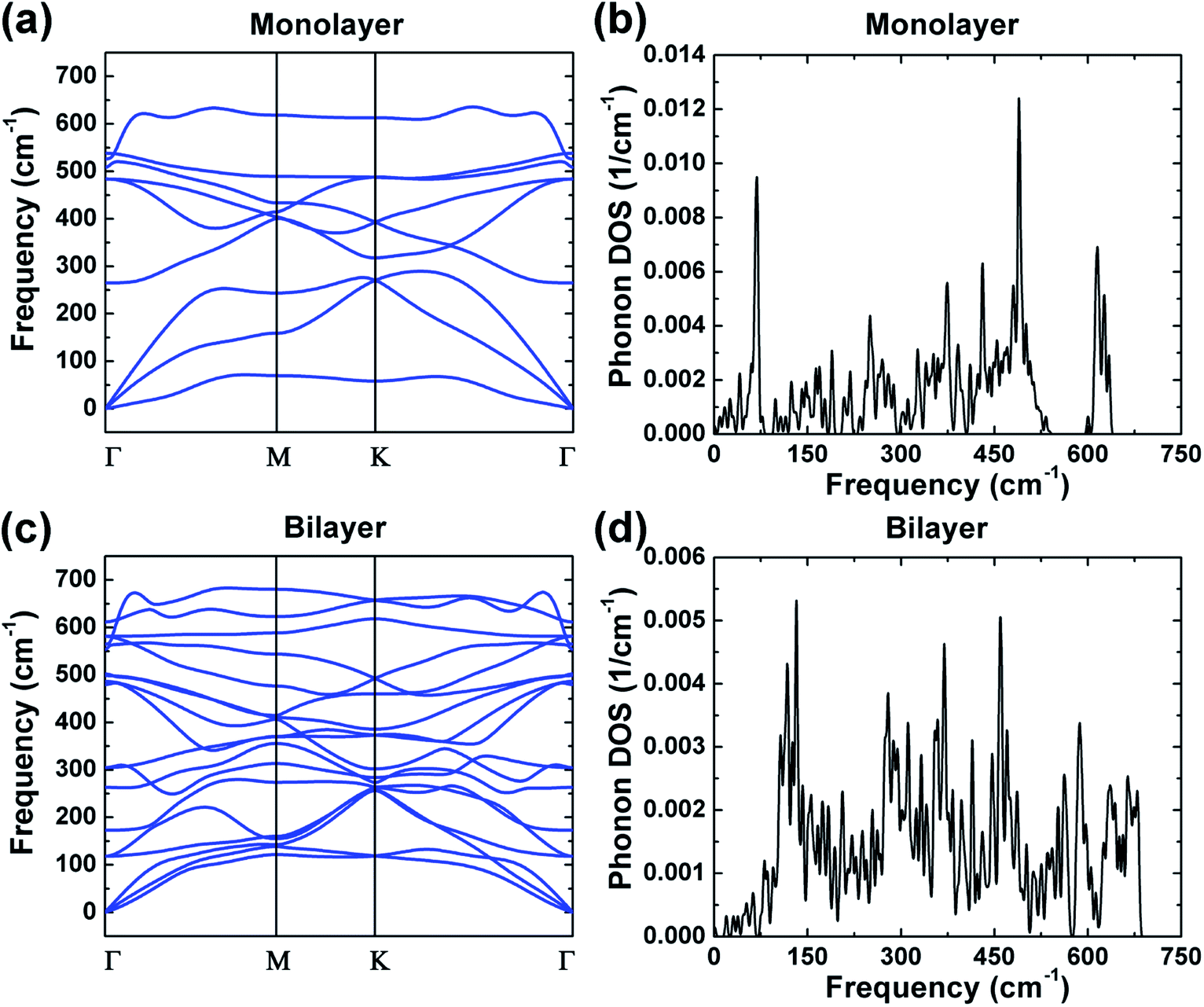 | ||
| Fig. 3 The phonon dispersions of the monolayer and bilayer 1T-ZrO2 are shown in (a) and (c), respectively; the phonon density of states are exhibited in (b) and (d). | ||
Combined with the phonon dispersions, the analysis of the phonon DOS of monolayer ZrO2 (Fig. 3b) demonstrates that the peak at 68.3 cm−1 is entirely contributed by the acoustics branches of phonon. It is noteworthy that the acoustic branches and the optical branches are separated by a gap of about 10 cm−1 in the frequency range of 83.0–93.0 cm−1. There is also a gap of about 46 cm−1 between the acoustic and optical branches of monolayer 1T-HfO2.39 In addition, a gap of about 51 cm−1 appeared in the frequency range of 543 and 594 cm−1 (the optical branches). However, from the phonon DOS of the bilayer exhibited in Fig. 3d, compared to the monolayer, we did not find a gap between the optical branches and the acoustic branches. Through the phonon dispersion of the bilayer ZrO2 (Fig. 3c), it can be found that the acoustic branches and the optical branches cross over, which further illustrates the above results. The absence of a gap between the acoustic and optical branches in bilayer ZrO2 may be attributed to the low-frequency optical modes of two monolayers against each other. The phenomenon of a gap between acoustic and optical branches appearing in the monolayer but disappearing in the bilayer can also be found in 2H-MoS2. For the bilayer and bulk 2H-MoS2, the low-frequency optical modes appearing due to the rigid-layer shear and vertical motion almost match the acoustic modes as the wavenumber q increases.35,42 However, the low-frequency optical modes are absent in monolayer 2H-MoS2 as the rigid-layer shear and vertical motions do not exist, and the acoustic and optical branches are separated by a gap of about 50 cm−1.43
Two possible routes to preparing monolayer and bilayer ZrO2 are through hard-bond cleavage and epitaxial growth. In literature reports, some freestanding monolayers and few-layers have been successfully acquired from non-layered bulk solids by means of various experimental techniques.44,45 For example, monolayer γ-Ga2O3 nanosheets have been prepared from the cubic spinel-type structure via a facile hydrothermal method,44 and large-area freestanding ZnSe monolayers have been fabricated from the zinc-blende ZnSe by means of a strategy involving a lamellar hybrid intermediate.45 The reported experimental preparations of 2D materials from bulk phases demonstrate that the monolayer or few-layer ZrO2 can probably be fabricated from the cubic ZrO2 via some experimental hard-bond cleavage methods. Furthermore, epitaxial growth on a selected substrate can also be a feasible route to prepare the monolayer or few-layer ZrO2. Recently, it was reported that ZrO2 films on a Rh (111) substrate with thicknesses in the range of 2–10 monolayers were deposited using a UHV-compatible sputter source, resulting in layer-by-layer growth and good homogeneity of the films.37 The films showed a (2 × 1) or a distorted (2 × 2) surface structure with respect to the cubic ZrO2 (111) crystal plane,37 which is consistent with the predicted structure of the monolayer and bilayer ZrO2 in our study. Moreover, the lattice constants of layered MoSe2 and WSe2 were 3.288 and 3.286 Å, respectively,46 which well match the lattice constant of monolayer ZrO2 (3.28 Å), and thus can also be candidates for epitaxial substrates.
Electronic structures of the monolayer and bilayer ZrO2
Electronic band structures of monolayer and bilayer ZrO2 along the high-symmetry lines (Γ–M–K–Γ) in the first Brillouin zone were calculated by GGA-PBE exchange–correlation functional in the CASTEP code, as shown in Fig. 4a and c, respectively. From Fig. 4a, the band structure of monolayer ZrO2 possesses a band gap of 4.51 eV, with the conduction band minimum (CBM) located at the K point and the valence band maximum (VBM) located between the K and Γ points, which indicate that the monolayer ZrO2 is an insulator with an indirect and wide band gap. However, compared to the monolayer, the CBM of the bilayer ZrO2 is located at the high symmetry point Γ, and the VBM is between the high symmetry points Γ and M (as shown in Fig. 4c). Moreover, although the band gap of the bilayer ZrO2 is 4.08 eV, reduced by 0.43 eV as compared to that of the monolayer, the bilayer ZrO2 is still an insulator possessing an indirect and wide band gap. The total DOS and partial DOS (PDOS) of the monolayer ZrO2 were also calculated by GGA-PBE, as depicted in Fig. 4b. From the analysis of PDOS, O 2p orbitals have significant contributions to valence bands (−3.92 to 0 eV), and the Zr 4d orbitals possess contributions of similar magnitude to O 2p in the energy range −3.92 to −2.21 eV but less significant near the VBM, demonstrating that O 2p and Zr 4d orbitals hybridize in the range −3.92 to –2.21 eV. Electronic states within the 1 eV range below the VBM are dominated by O 2p, whereas the low conduction bands are dominated by Zr 4d orbitals (in the energy range 4.51–6.31 eV). There is only one equivalent oxygen atom for the monolayer ZrO2, but for the bilayer ZrO2, there are two inequivalent oxygen atoms (O1 and O2) as indicated in the side view of the bilayer in Fig. 1b. From the analysis of PDOS of the bilayer (Fig. 4d), the electronic states near the VBM are dominated by both O1 2p and O2 2p. In the energy range −3.47 to −0.76 eV, O1 2p orbitals possess more contributions than O2 2p orbitals, whereas, in the energy range of −5.0 to −3.47 eV, the contributions of O2 2p orbitals are much larger than that of O1 2p orbitals, reflecting the different chemical environments of O1 (bonded with three Zr atoms in one layer) and O2 (bonded with not only three Zr atoms in one layer but also one Zr atom in the adjacent layer). The low conduction bands (in the energy range 4.08–6.50 eV) are dominated by Zr 4d orbitals, the same as monolayer ZrO2.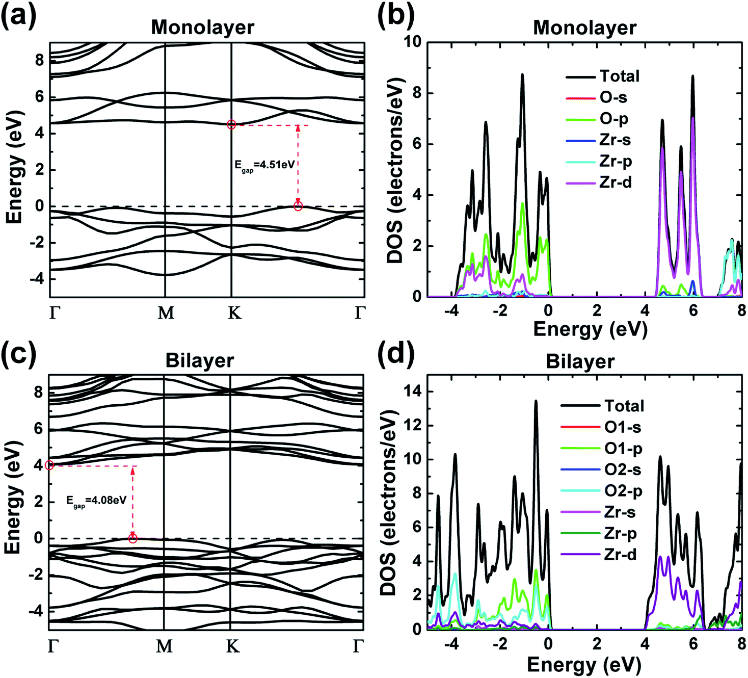 | ||
| Fig. 4 The electronic band structures and the density of states (DOS) of the 1T-ZrO2 monolayer (a and b) and bilayer (c and d), respectively, calculated by the GGA-PBE exchange–correlation functional. The valence band maximum was set to 0 eV. | ||
The DOS features of monolayer and bilayer ZrO2 are different. The major peaks of the total DOS of monolayer ZrO2 are located at −3.15, −2.59, −1.08, −0.35 and −0.07 eV, respectively (in the high energy region of the valence band), and the peak at −1.08 eV is the most prominent. For bilayer ZrO2, the major peaks of the total DOS are located at −4.56, −3.85, −2.90, −1.39, −0.52 and −0.06 eV, respectively (in the high energy region of the valence band), and the highest peak is located at −0.52 eV higher than that of the monolayer (−1.08 eV), as shown in Fig. 4d. Different fine structures of DOS will result in distinguishable spectral features using techniques probing the occupied and unoccupied electronic states, such as X-ray absorption spectroscopy (XAS), X-ray emission spectroscopy (XES), and electron energy-loss spectroscopy (EELS). Excited electron and hole states have different characteristics for both monolayer and bilayer ZrO2 as the unoccupied states near the CBM are dominated by Zr 4d and the occupied electronic states near the VBM are dominated by O 2p.
Since it is well known that standard DFT using LDA/GGA will underestimate the band gap, we have also calculated the band gap of ZrO2 polymorphs and 2D ZrO2 using the GW method implemented in the ABINIT code. The DFT-GGA and GW band gaps calculated by the ABINIT code are listed in Table 2 and the corresponding band structures are provided in the ESI (Fig. S1†). DFT-GGA band gaps calculated by CASTEP are also listed for comparison. Note that the reported experimental band gaps of bulk ZrO2 are spread in a quite large range, especially for cubic and tetragonal phases,47–51 which may have arisen from the difference in the stabilizer and the crystalline morphology. Our calculated GW band gaps are close to, or in the range of, reported experimental band gaps for bulk ZrO2 polymorphs. GW band gaps of monolayer and bilayer ZrO2 are 7.51 and 6.82 eV, respectively, larger than those of all the bulk phases of ZrO2 and h-BN (5.97 eV).18
| Band gap (eV) | ||||
|---|---|---|---|---|
| GGA-PBE (CASTEP) | GGA-PBE (ABINIT) | GW | Experiment | |
| a Experiment ref. 47.b Experiment ref. 48.c Experiment ref. 49.d Experiment ref. 50.e Experiment ref. 51. | ||||
| Monolayer | 4.51 | 4.82 | 7.51 | NA |
| Bilayer | 4.08 | 4.48 | 6.82 | NA |
| Cubic | 3.47 | 4.10 | 5.01 | 4.96a, 6.10b |
| Tetragonal | 4.16 | 4.50 | 5.98 | 5.78b, 5.0c |
| Monoclinic | 3.78 | 3.84 | 5.34 | 5.30c, 4.99d, 5.20e |
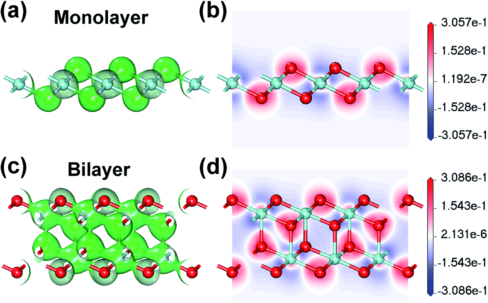
In order to describe the covalency and ionicity of the atomic bonds and the electron transfer between atoms, the electron density and the electron density difference (Δρ) of monolayer and bilayer ZrO2 have been calculated. For the monolayer ZrO2, the isosurfaces of the electron density at the value of about 0.60 electrons per Å3 and the slice through the map of the electron density difference are depicted in Fig. 5a and b, respectively. In the isosurfaces of the electron density of the monolayer ZrO2 (Fig. 5a), the electron density between the O and Zr atoms was about 0.60 electrons per Å3, revealing that there are shared electrons between the O and Zr atoms and the O–Zr bond has a covalent component. From the slice of the electron density difference (Fig. 5b), the electrons are depleted around the Zr atoms (the maximum value of the depleted electrons is −0.31 electrons per Å3), but accumulate around the O atoms (the maximum value of the accumulated electrons is 0.26 electrons per Å3) with the transferred electrons localized around the O atoms, which indicates that the O–Zr bond has strongly ionic character. For the bilayer ZrO2, the isosurface of the electron density at the value of about 0.45 electrons per Å3 and the slice through the map of the electron density difference are shown in Fig. 5c and d, respectively. From the isosurfaces of the electron density and the electron density difference of the bilayer ZrO2, similar to the monolayer ZrO2, the O–Zr bond also has both covalent and ionic characteristics. It is worth noting that the interlayer bond of the bilayer ZrO2 is strong, with a corresponding electron density of about 0.45 electrons per Å3 in the middle of the interlayer Zr–O bond, which is in contrast to the weak vdW interlayer interaction in TMDs.
 | ||
| Fig. 5 The isosurfaces of the electron density of the 1T-ZrO2 monolayer and bilayer at the values of (a) about 0.60 electrons per Å3 and (c) about 0.45 electrons per Å3, respectively. The side view showing the slices through the maps of the electron density difference of 1T-ZrO2 monolayer and bilayer are depicted in (b) and (d), respectively. | ||
Static dielectric constant calculation
For the investigations of the dielectric properties of monolayer and bilayer ZrO2, the macroscopic static dielectric constants containing both the ionic and the electronic response were calculated by the DFPT formalism in response to the electric field. In our previous study, a practical method for accurately evaluating the dielectric constants of 2D materials based on the calculated value obtained from a supercell containing the 2D materials and a vacuum slab have been proposed,39 which is similar to that obtained by Laturia et al. based on the equivalent capacitance principle, but from a different point of view.23 The formula for calculating the dielectric constant of 2D materials based on the corresponding static dielectric constants of the supercell is as follows:23,39
 | (2) |
 | (3) |
For the monolayer, the lattice constant c of the supercell employed in the DFPT calculation is 28 Å, and the static dielectric constant from the supercell calculation are εs‖ = 6.14 and εs⊥ = 1.15, respectively. Based on eqn (2) and (3), we determined that the in-plane and out-of-plane static dielectric constants of monolayer ZrO2 are εm‖ = 33.34 and εm⊥ = 5.58, respectively. For the bilayer, the lattice constant c of the supercell is 35 Å in the DFPT calculation, and the static dielectric constant from the supercell calculation are εs‖ = 7.92 and εs⊥ = 1.23, respectively. In a similar way, we determined that the in-plane and out-of-plane static dielectric constants of the bilayer of 1T-ZrO2 are εb‖ = 33.86 and εb⊥ = 8.93, respectively. Interestingly, the static dielectric constant of the bilayer (εb‖ = 33.86) along the in-plane direction only increased by 1.56% as compared to that of the monolayer (εm‖ = 33.34), but the static dielectric constant of the bilayer (εb⊥ = 8.93) along the out-of-plane direction remarkably increased by 60% as compared to that of the monolayer (εm⊥ = 5.58), indicating that increasing the number of layers of 1T-ZrO2 has a negligible effect on the in-plane static dielectric constant, while the static dielectric constant along the out-of-plane direction is significantly influenced by the number of layers.
Electronic properties and band edge alignment of the 2D ZrO2–MoS2 heterojunction
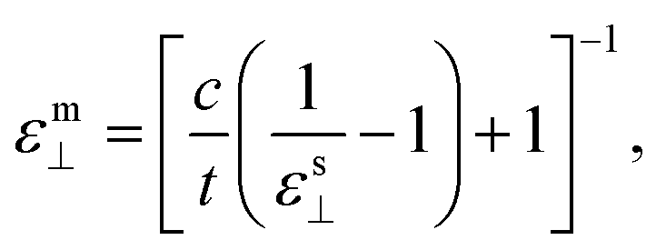
The structure and electronic structure of the interface between few-layered ZrO2 and layered MoS2 is important for the design of 2D electronic devices and for the possible growth of few-layered ZrO2 on the MoS2 substrate. MoS2 is semiconducting in a 2H layer but metallic in a 1T layer. Herein, we studied the electronic properties in the 2D heterojunction between monolayer ZrO2 and monolayer 2H-MoS2 by calculating the electron density difference and analyzing the electronic DOS. The electron density difference (Δρ) can be used to describe the electron transfer at the interface of a heterojunction, which is defined as the difference in electron-density between the states after and before the formation of the ZrO2–MoS2 heterojunction. The isosurfaces of the difference density at a value of about ±0.001 electrons per Å3 are shown in Fig. 6a. It can be seen that the transfer and aggregation of electrons mainly occur at the interface of the ZrO2–MoS2 heterojunction. At the interface of the heterojunction, electrons are transferred from the surrounding area of the sulfur atom and the oxygen atom to the MoS2–ZrO2 interlamination, forming weak bonds between the MoS2–ZrO2 interlamination. It is worth noting that the electrons depleted around S atoms are more pronounced than those of O atoms. We can gain further insight into the changes in bonding by displaying the density difference as a 2D slice, as shown in Fig. 6c. Moreover, in this plot, a loss of electrons is indicated in blue, while electron enrichment is indicated in red. From the electron density difference map, it is obvious that the electrons are depleted in the laminates of 2H-MoS2 and 1T-ZrO2, but accumulate in the MoS2–ZrO2 interlamination. | ||
| Fig. 6 (a) The isosurface of the difference density at a value of about ±0.001 electrons per Å3 for difference density heterojunction between 2H-MoS2 and 1T-ZrO2 monolayers. One is at +0.001 electrons per Å3 and is colored green, the other is at −0.001 electrons per Å3 and is colored purple. (b) The top view of the structural image and the blue line denoting the site of the slice. (c) The side view showing the slices through the map of the electron density difference of 2D ZrO2–MoS2 heterojunction. | ||
In order to characterize the source of the occupied electron contribution near the VBM in the 2D ZrO2–MoS2 heterojunction, we calculated the electron density distribution of the highest occupied orbitals (−1.14 to 0 eV), and the isosurface of the electron density at a value of about 0.06 electrons per Å3 is shown in Fig. 7a. We can find that the electrons of the occupied orbital state near the VBM are mainly from the Mo atoms, and a small part is from the S atoms. It is worth noting that the contribution of ZrO2 to the VBM in the 2D ZrO2–MoS2 heterojunction is nearly zero. We further characterized the contribution to the occupied electronic states near the VBM and the unoccupied states near the CBM by the calculations and analysis of the DOS. From the total DOS of the ZrO2–MoS2 heterojunction depicted in Fig. 7b, it can also be seen that the contributions to the occupied states near the VBM and unoccupied states near the CBM are entirely from MoS2; from ZrO2 there is almost no contribution.
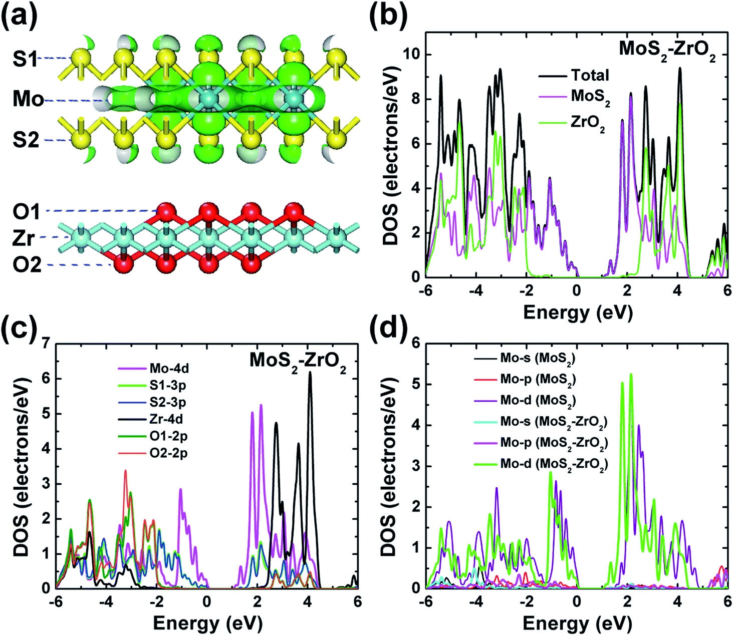 | ||
| Fig. 7 (a) The electron density distribution of the occupied orbitals (−1.14 to 0 eV) near the VBM, and the isosurface of the electron density at a value of about 0.06 electrons per Å3. (b) The calculated total DOS of the 2D ZrO2–MoS2 heterojunction. The calculated PDOS of (c) the 2D ZrO2–MoS2 heterojunction (only the main electronic orbitals are displayed) and (d) MoS2 (in the ZrO2–MoS2 heterojunction) and freestanding monolayer MoS2. | ||
The PDOS of the 2D ZrO2–MoS2 heterojunction is shown in Fig. 7c to further reveal the atomic specific contributions of electronic states. For clarity, only the main electronic orbitals are displayed in Fig. 7c; we refer to Fig. S2 in the ESI† for completeness. As indicated in Fig. 7a, oxygen and sulfur atoms are not equivalent after the formation of the interface due to their different locations at the interface sites (O1 and S1) or surface sites (O2 and S2), and the PDOS of inequivalent O or S atoms only differ very slightly (Fig. 7c). Both the electronic states near the CBM and VBM are dominated by contributions of Mo 4d orbitals, and the S 3p orbitals have a visible contribution to the electronic state near the VBM. In addition, the O 2p orbitals have a prominent contribution in the low valence bands (in the energy range −6 to −2 eV), and the main contributions of Zr and O to the conduction bands are in the energy range of 2.60–4.50 eV.
The band gap in the ZrO2–MoS2 heterojunction is mainly determined by the band gap of MoS2 as discussed above, and ZrO2 has a limited influence on the electronic state of the semiconductor MoS2 in the heterojunction system; therefore, ZrO2 can be used as an excellent dielectric material. However, the calculated band gap of monolayer MoS2 in the heterojunction is 1.16 eV, which is significantly smaller than the band gap of the freestanding monolayer MoS2 (1.60 eV). In order to analyze the causes of the above phenomenon, we compared the PDOS of monolayer MoS2 in the heterojunction with the freestanding monolayer MoS2 in Fig. 7d. In addition to the overall translation to the left for the conduction bands of the heterojunction, which is connected to the decrease in the band gap, the detailed fine features of Mo 4d also changed, especially the relative weight in the energy ranges near the band gap as compared to those of the freestanding monolayer MoS2.
For a 2D heterojunction formed by monolayer MoS2 and ZrO2, the electron affinity rule fails and the band gaps and band edge positions of the two component monolayers will be altered by each other. As shown in Fig. 8a, the CBM energy relative to the vacuum level of the freestanding MoS2 and ZrO2 monolayers are −4.25 eV and −3.29 eV, respectively, and their band gaps are 1.60 eV and 4.51 eV, respectively. After a heterojunction between the MoS2 and ZrO2 monolayer is formed (Fig. 8b), the CBM of MoS2 shifts down to −4.55 eV relative to the vacuum level and the band gap is 1.16 eV, which is smaller than the freestanding MoS2 (as discussed above). To aid a quantitative analysis, the VBM and CBM band edge positions of ZrO2 in the heterojunction were approximately deduced from the PDOS of Zr atoms and the outermost O atoms (denoted as O2 in Fig. 7a) and it was found that the VBM of ZrO2 slightly shifted upwards, resulting in a smaller band gap (4.22 eV) as compared to the freestanding monolayer ZrO2. The electron affinity energy of the heterojunction was determined by the ZrO2 part and was only slightly larger than that of the freestanding monolayer ZrO2. The offset of the band edges after forming the heterojunction is consistent with the physical picture that the separate chemical potentials tend to merge after the interface was formed. The realignment of the band edges is related to the electron transfer discussed in Fig. 6, i.e., electrons are accumulated at the interface formed by MoS2 and ZrO2. The large band gap of monolayer ZrO2 and the type I heterojunction formed with monolayer MoS2 is beneficial for confining carriers in the MoS2 semiconductor.
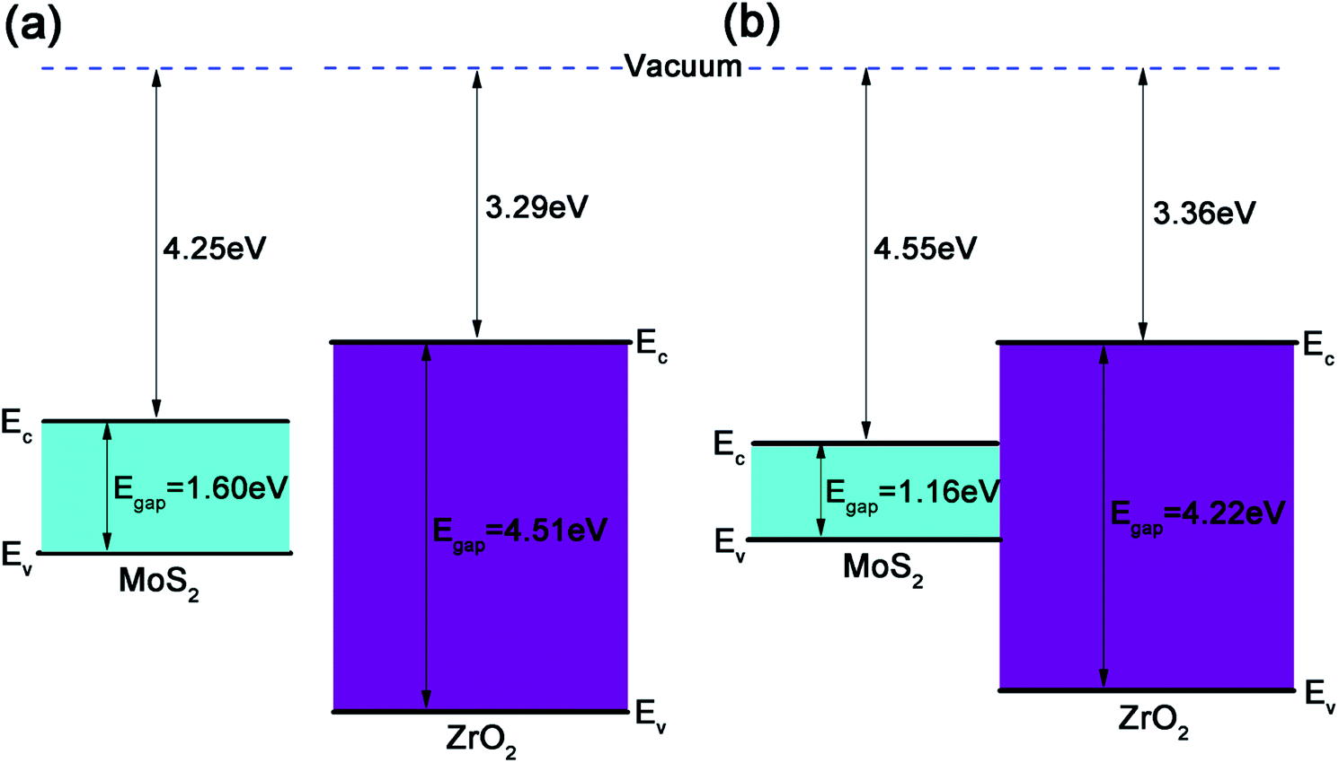 | ||
| Fig. 8 (a) Band edge positions of separating MoS2 and ZrO2 monolayers. (b) Band edge diagram of the 2D ZrO2–MoS2 heterojunction. | ||
Conclusion
The structure and properties of ZrO2 in the ultrathin limit (monolayer and bilayer) were investigated. We have shown that both monolayer and bilayer ZrO2 adopt a honeycomb-like structure, which is similar to 1T-MoS2. The stability of monolayer and bilayer ZrO2 with the 1T structure was confirmed by the calculations of enthalpies of formation and phonon dispersions. The 1T-ZrO2 monolayer or bilayer can be fabricated by the cleavage from the (111) facet of non-layered cubic ZrO2 or by epitaxial growth on a carefully selected substrate such as layered TMDs. Our observation that the in-plane lattice constants of the monolayer and bilayer were shrunken as compared to the corresponding slab in cubic ZrO2 is consistent with the experimental results of the ultrathin ZrO2 films grown on the Rh (111) substrate or formed by oxidation of the Pt3Zr (0001) surface. The calculated electronic band gaps calculated from the GW method show that both the monolayer and bilayer ZrO2 have large band gaps, reaching 7.51 eV and 6.82 eV, respectively. The static dielectric constant of the bilayer ZrO2 (εb‖ = 33.86) along the in-plane direction only increased by 1.56% as compared to that of the monolayer (εm‖ = 33.34), while the static dielectric constant of the bilayer (εb⊥ = 8.93) along the out-of-plane direction was remarkably increased by 60% as compared to that of the monolayer (εm⊥ = 5.58), indicating that the increasing number of layers of 1T-ZrO2 has a more significant effect for the static dielectric constant along the out-of-plane direction. In addition, the static dielectric constants of both monolayer and bilayer are larger as compared to those of monolayer h-BN (ε‖ = 6.82, ε⊥ = 3.29). Therefore, 1T-ZrO2 is a promising candidate for applications in 2D FETs and heterojunctions, due to the high dielectric constant, good thermodynamic stability, and large band gap. The interface between monolayer ZrO2 and monolayer MoS2 was studied and it has been shown that a type I heterojunction was formed. The electronic states near the VBM and CBM of the heterojunction are dominated by the contributions from monolayer MoS2, and the band gap of the monolayer MoS2 interfaced with monolayer ZrO2 is smaller than its freestanding counterparts.Conflicts of interest
There are no conflicts to declare.Acknowledgements
This study was supported by the Innovation Program of Shanghai Municipal Education Commission (Grant No. 15ZZ001) and the Natural Science Foundation of Shanghai (Grant No. 19ZR1404300).Notes and references
- F. Schwierz, Nat. Nanotechnol., 2010, 5, 487 CrossRef CAS PubMed.
- Q. H. Wang, K. Kalantar-Zadeh, A. Kis, J. N. Coleman and M. S. Strano, Nat. Nanotechnol., 2012, 7, 699 CrossRef CAS.
- B. Radisavljevic, A. Radenovic, J. Brivio, i. V. Giacometti and A. Kis, Nat. Nanotechnol., 2011, 6, 147 CrossRef CAS.
- S. Yu, J. S. Kim, P. J. Jeon, J. Ahn, J. C. Park and S. Im, Adv. Funct. Mater., 2017, 27, 1603682 CrossRef.
- Y. Hu, H. Jiang, K. M. Lau and Q. Li, Semicond. Sci. Technol., 2018, 33, 045004 CrossRef.
- Y. Cui, R. Xin, Z. Yu, Y. Pan, Z. Y. Ong, X. Wei, J. Wang, H. Nan, Z. Ni and Y. Wu, Adv. Mater., 2015, 27, 5230–5234 CrossRef CAS.
- D. Deng, K. Novoselov, Q. Fu, N. Zheng, Z. Tian and X. Bao, Nat. Nanotechnol., 2016, 11, 218 CrossRef CAS.
- S. Li, S. Wang, M. M. Salamone, A. W. Robertson, S. Nayak, H. Kim, S. E. Tsang, M. Pasta and J. H. Warner, ACS Catal., 2016, 7, 877–886 CrossRef.
- S. Das, Sci. Rep., 2016, 6, 34811 CrossRef CAS.
- H. Liu, A. T. Neal, Z. Zhu, Z. Luo, X. Xu, D. Tománek and P. D. Ye, ACS Nano, 2014, 8, 4033–4041 CrossRef CAS.
- T. Roy, M. Tosun, J. S. Kang, A. B. Sachid, S. B. Desai, M. Hettick, C. C. Hu and A. Javey, ACS Nano, 2014, 8, 6259–6264 CrossRef CAS.
- X. Liu, Y. Chai and Z. Liu, Nanotechnology, 2017, 28, 164004 CrossRef.
- V. Perebeinos, J. Tersoff and P. Avouris, Phys. Rev. Lett., 2004, 92, 257402 CrossRef.
- L. Zeng, Z. Xin, S. Chen, G. Du, J. Kang and X. Liu, Appl. Phys. Lett., 2013, 103, 113505 CrossRef.
- N. Ma and D. Jena, Phys. Rev. X, 2014, 4, 011043 Search PubMed.
- S.-L. Li, K. Wakabayashi, Y. Xu, S. Nakaharai, K. Komatsu, W.-W. Li, Y.-F. Lin, A. Aparecido-Ferreira and K. Tsukagoshi, Nano Lett., 2013, 13, 3546–3552 CrossRef CAS.
- T. Fang, A. Konar, H. Xing and D. Jena, Phys. Rev. B: Condens. Matter Mater. Phys., 2008, 78, 205403 CrossRef.
- L. Wang, B. Wu, J. Chen, H. Liu, P. Hu and Y. Liu, Adv. Mater., 2014, 26, 1559–1564 CrossRef CAS.
- Y. A. Wu, A. I. Kirkland, F. Schäffel, K. Porfyrakis, N. P. Young, G. A. D. Briggs and J. H. Warner, Nanotechnology, 2011, 22, 195603 CrossRef.
- J. Sun, C. Lu, Y. Song, Q. Ji, X. Song, Q. Li, Y. Zhang, L. Zhang, J. Kong and Z. Liu, Chem. Soc. Rev., 2018, 47, 4242–4257 RSC.
- D. Jena and A. Konar, Phys. Rev. Lett., 2007, 98, 136805 CrossRef PubMed.
- A. Konar and D. Jena, J. Appl. Phys., 2007, 102, 123705 CrossRef.
- A. Laturia, M. L. Van de Put and W. G. Vandenberghe, npj 2D Mater. Appl., 2018, 2, 6 CrossRef.
- E. H. Kisi and C. Howard, Key Eng. Mater., 1998, 153, 1–36 Search PubMed.
- S. Fabris, A. T. Paxton and M. W. Finnis, Acta Mater., 2002, 50, 5171–5178 CrossRef CAS.
- A. Mirgorodsky, M. Smirnov and P. Quintard, Phys. Rev. B: Condens. Matter Mater. Phys., 1997, 55, 19 CrossRef CAS.
- F. Schwierz, J. Pezoldt and R. Granzner, Nanoscale, 2015, 7, 8261–8283 RSC.
- C. Ataca, H. Sahin and S. Ciraci, J. Phys. Chem. C, 2012, 116, 8983–8999 CrossRef CAS.
- S. J. Clark, M. D. Segall, C. J. Pickard, P. J. Hasnip, M. I. Probert, K. Refson and M. C. Payne, Z. für Kristallogr. - Cryst. Mater., 2005, 220, 567–570 CAS.
- B. G. Pfrommer, M. Côté, S. G. Louie and M. L. Cohen, J. Comput. Phys., 1997, 131, 233–240 CrossRef CAS.
- S. Grimme, J. Comput. Chem., 2006, 27, 1787–1799 CrossRef CAS.
- S. Baroni, S. De Gironcoli, A. Dal Corso and P. Giannozzi, Rev. Mod. Phys., 2001, 73, 515 CrossRef CAS.
- X. Gonze, B. Amadon, P.-M. Anglade, J.-M. Beuken, F. Bottin, P. Boulanger, F. Bruneval, D. Caliste, R. Caracas and M. Côté, Comput. Phys. Commun., 2009, 180, 2582–2615 CrossRef CAS.
- M. Fuchs and M. Scheffler, Comput. Phys. Commun., 1999, 119, 67–98 CrossRef CAS.
- A. Molina-Sanchez and L. Wirtz, Phys. Rev. B: Condens. Matter Mater. Phys., 2011, 84, 155413 CrossRef.
- S. L. Xiao, W. Z. Yu and S. P. Gao, Surf. Sci., 2016, 653, 107–112 CrossRef CAS.
- P. Lackner, Z. Zou, S. Mayr, J.-I. J. Choi, U. Diebold and M. Schmid, Surf. Sci., 2019, 679, 180–187 CrossRef CAS.
- M. Antlanger, W. Mayr-Schmölzer, J. Pavelec, F. Mittendorfer, J. Redinger, P. Varga, U. Diebold and M. Schmid, Phys. Rev. B: Condens. Matter Mater. Phys., 2012, 86, 035451 CrossRef.
- J. Weng and S.-P. Gao, Phys. Chem. Chem. Phys., 2018, 20, 26453–26462 RSC.
- A. Jain and A. J. McGaughey, Sci. Rep., 2015, 5, 8501 CrossRef CAS.
- K. Kaasbjerg, K. Bhargavi and S. Kubakaddi, Phys. Rev. B: Condens. Matter Mater. Phys., 2014, 90, 165436 CrossRef.
- G. Q. Huang, Z. W. Xing and D. Y. Xing, Phys. Rev. B, 2016, 93, 104511 CrossRef.
- Y. Q. Cai, J. H. Lan, G. Zhang and Y. W. Zhang, Phys. Rev. B: Condens. Matter Mater. Phys., 2014, 89, 035438 CrossRef.
- Y. Sun, Z. Sun, S. Gao, H. Cheng, Q. Liu, J. Piao, T. Yao, C. Wu, S. Hu and S. Wei, Nat. Commun., 2012, 3, 1057 CrossRef.
- X. Zhang, Z. Zhang, J. Liang, Y. Zhou, Y. Tong, Y. Wang and X. Wang, J. Mater. Chem. A, 2017, 5, 9702–9708 RSC.
- J. A. Wilson and A. Yoffe, Adv. Phys., 1969, 18, 193–335 CrossRef CAS.
- D. Prakashbabu, R. H. Krishna, B. Nagabhushana, H. Nagabhushana, C. Shivakumara, R. Chakradar, H. Ramalingam, S. Sharma and R. Chandramohan, Spectrochim. Acta, Part A, 2014, 122, 216–222 CrossRef CAS.
- R. H. French, S. Glass, F. Ohuchi, Y.-N. Xu and W. Ching, Phys. Rev. B: Condens. Matter Mater. Phys., 1994, 49, 5133 CrossRef CAS.
- L. Dash, N. Vast, P. Baranek, M.-C. Cheynet and L. Reining, Phys. Rev. B: Condens. Matter Mater. Phys., 2004, 70, 245116 CrossRef.
- J. Bendoraitis and R. Salomon, J. Phys. Chem., 1965, 69, 3666–3667 CrossRef CAS.
- C. K. Kwok and C. R. Aita, J. Appl. Phys., 1989, 66, 2756–2758 CrossRef CAS.
Footnote |
| † Electronic supplementary information (ESI) available. See DOI: 10.1039/c9ra06074j |
| This journal is © The Royal Society of Chemistry 2019 |