
 Open Access Article
 This Open Access Article is licensed under a Creative Commons Attribution-Non Commercial 3.0 Unported Licence
Understanding the enhanced electrical properties of free-standing graphene paper: the synergistic effect of iodide adsorption into graphene†
R. Karthicka,
Xianhua Houa,
Qiang Rua,
S. Selva Chandrasekaranb,
M. Ramesh *b and
Fuming Chen*a
*b and
Fuming Chen*a
aGuangdong Provincial Key Laboratory of Quantum Engineering and Quantum Materials, Guangdong Engineering Technology Research Center of Efficient Green Energy, Environment Protection Materials, School of Physics and Telecommunication Engineering, South China Normal University, Guangzhou 510006, P. R. China. E-mail: fmchen@m.scnu.edu.cn
bFunctional Materials Division, CSIR-Central Electrochemical Research Institute, Karaikudi 600003, TamilNadu, India. E-mail: ramesh_pondi@yahoo.co.in
First published on 21st October 2019
Abstract
Free-standing graphene (FSG) paper plays a vital role in a wide variety of applications as an electrode material. Specifically, the electrical properties of FSG are the most important factor affecting its use as an electrode material. Herein, the vacuum filtration technique is utilized to fabricate GO paper, which is then reductively treated with HI. Initially, the electrical conductivity is measured for GO papers with different thicknesses by varying the concentration of GO precursor as well as the reduction time. The FSG paper with a thickness of 3 microns exhibits the lowest sheet resistance and further characterization is carried out to reveal the origin of this enhancement of electrical properties. The low resistance is attributed to its crystalline nature, stacking height (Lc), in-plane crystallite size (La) and defect density (nD). Meanwhile, iodide ions intercalated into the graphene layers act as hole-carriers, and their intercalation is favoured over adsorption at the surface.
1. Introduction
Graphene, i.e. 2D carbon sheets, is a promising candidate in a wide variety of applications, especially graphene-based electrodes for electronic, optoelectronic and electrochemical devices, due to the remarkable properties of graphene.1 Among the graphene family, free-standing graphene (FSG) paper-like electrodes are experiencing rapid growth in popularity for energy storage and conversion applications for flexible devices.2 Nevertheless, bare FSG paper as an electrode provides poor electrochemical behaviour. Hence, it is often incorporated or composited with an electrochemically active host material to enhance the device performance.3 The enhanced performance observed in FSG hybrid paper is due to its high electrical conductivity as well as its ability to collect or withdraw electrons effectively from/to electrochemically active materials. FSG is prepared by various approaches based on the precursor choice.4,5 Commonly, graphene oxide (GO) is preferred as a precursor owing to large scale processability and dispersibility in many solvents, which in turn is due to abundant functional groups, and hence it is utilized for GO paper preparation.6Generally, GO paper shows very low electrical conductivity and also has higher mechanical strength than other paper-like materials.7 GO as an insulator can be converted into highly conductive graphene paper by several techniques. Generally, reductive treatment is preferred to thermal or chemical routes as it allows complete restoration of sp2 carbon without any defects. It is well known that the performances of graphene electrodes in electronic devices are based on the electrical properties, which are greatly influenced by the synthetic methods, as these introduce several changes in the structure and the extent of reduction (ratio of C/O).8 Reductive chemical treatment efficiently removes the oxygen moieties from GO paper whereas thermal treatment provides good restoration of the sp2 carbon network but less removal of oxygen functional groups.9,10 Upon exposure of GO paper to hydrazine vapour, the electrical conductivity of GO paper increases by four orders of magnitude from 8.5× 10⁻² S m−1 to 1.7 × 10² S m−1. Recently, a rapid reduction treatment was proposed in which GO papers are immersed in hydrohalic acids, viz., HI and HBr, and the treated papers showed remarkable electrical conductivity around 298 and 243 S cm−1 respectively.11,12 Further development in the electrical conductivity of FSG was obtained by reducing GO papers using metal halides like MgI2, AlI3, ZnI2, and FeI2, achieving conductivities up to 550 S cm−1.13
However, it is essential to reveal the original of the electrical property enhancement of GO paper during reduction for future electronic device fabrication. Herein, we have chosen HI acid as the reducing agent to reduce GO paper. After the reduction process, it is important to characterize the resulting defects, which directly impact the specific applications of GO paper. The electrical properties of HI-treated GO paper arise from the highly crystalline nature and restored sp2 network. Moreover, the variation of stacking height, in-plane crystallite size and defect density of FSG also affects the electrical behaviour after reduction treatment. A significant factor is the synergistic effect of the iodide ions that intercalate into FSG paper during reduction treatment. Hence, adjustment of the parameters that influence the electrical behaviour may be utilized for specific electronic device applications.
2. Experimental
Graphene oxide was prepared according to a previous report.14 GO powder was well dispersed in 5 mL of distilled water with different concentrations of 4, 8 and 10 mg mL−1 under a probe sonicator for 1 h. These three concentrations of GO were subjected to vacuum filtration to obtain homogeneous free-standing GO paper. The obtained GO papers were reduced by dipping them in HI solution for different intervals of 0.5, 1 and 24 h and denoted as FSG1, FSG2 and FSG3 respectively. All the samples were washed with pure ethanol and distilled water, followed by heating in a vacuum oven overnight before characterization.2.1 Characterization
Raman spectra of graphite and graphene oxide were obtained to characterize the surface defects and sp2 hybridization of the graphene sheets (RENISHAW, The Netherlands) at the excitation wavelength of 532 nm with exposure time of 10 s (100% intensity). The structures of the FSG papers were determined by using a PANALYTICAL (The Netherlands) powder diffractometer with Cu Kα (λ = 1.5406 Å) radiation at a scan speed of 2° min−1 and a step size of 0.03° in the range of 5° ≤ 2θ ≤ 90°. The functional groups were determined by FT-IR analysis with a BRUKER TENSOR 27 spectrometer in the wavenumber range of 4000–400 cm−1. Scanning electron microscopy (SEM) was used to observe the surface morphology and cross sectional images of the FSG papers (TESCAN, Czech Republic), with the magnification of 5000×. The electrical conductivities of the FSG samples were measured by a four-point probe (SES Instruments, India) attached to a PID controlled oven. The electrical properties and IV curves were measured by Hall effect measurement apparatus (ECOPIA-HMS, South Korea) by applying 1 mA current and 0.5 Tesla magnetic field. All the electrochemical characterizations were performed using an SP-150 instrument (Bio-Logic, France). The thickness of the FSG paper was measured by an ELCOMETER 456 ferrous substrate.3. Results and discussion
3.1 Reduction mechanism
The possible reduction mechanism of GO paper in HI solution is shown in Scheme S1.† GO colloidal solution was synthesised from graphite by the modified Hummers' method and filtered to obtain free-standing GO paper with controlled thickness by varying the GO concentration. As GO consists of epoxy, hydroxyl and carboxyl groups, it behaves as an insulator. When the GO paper was immersed in HI solution, the colour of the solution turned deep red, which implies a rapid reaction. During the process, the hydrogen of HI attacks the oxygen in an epoxy group, which forms an oxo cation and leaves behind an iodide ion on the graphene surface. The oxo cation of the epoxy ring splits into two hydroxyl groups and forms a C–I bond upon removal of a water molecule. Similar to the effect of HI on epoxy groups, a hydroxyl group is reduced upon elimination of a water molecule, leaving behind an iodide ion.15,16 These iodides react with one another to form iodine and further triiodide molecules and higher iodides. These polyiodide species are adsorbed on the surface/interior as well as being intercalated into the FSG paper. The iodide ions are strongly adsorbed on the graphene sheet surfaces of the FSG paper17,18 whereas the unreacted iodine molecules and HI are removed by treatment with ethanol solution several times.3.2 Effect of sheet resistance
Fig. 1(a) shows the variation of FSG sheet resistance (Rs) as a function of the thickness, which was tuned by varying the concentration of GO, and of the reduction time. GO powders with concentrations of 4, 8 and 10 mg mL−1 were well dispersed in 5 mL of distilled water under probe sonication for 1 h to fabricate GO paper followed by HI reduction. The thickness was measured at several points on the surface of the FSG paper using the Elcometer. For these measurements, the FSG papers were sliced into several pieces and cross sectional images were captured. By averaging the thicknesses obtained by the Elcometer and cross-sectional imaging, an approximate thickness was obtained. The cross-sectional SEM images in Fig. 1(b), (c) and (d) show distinct differences in the extent of stacking at various GO concentrations.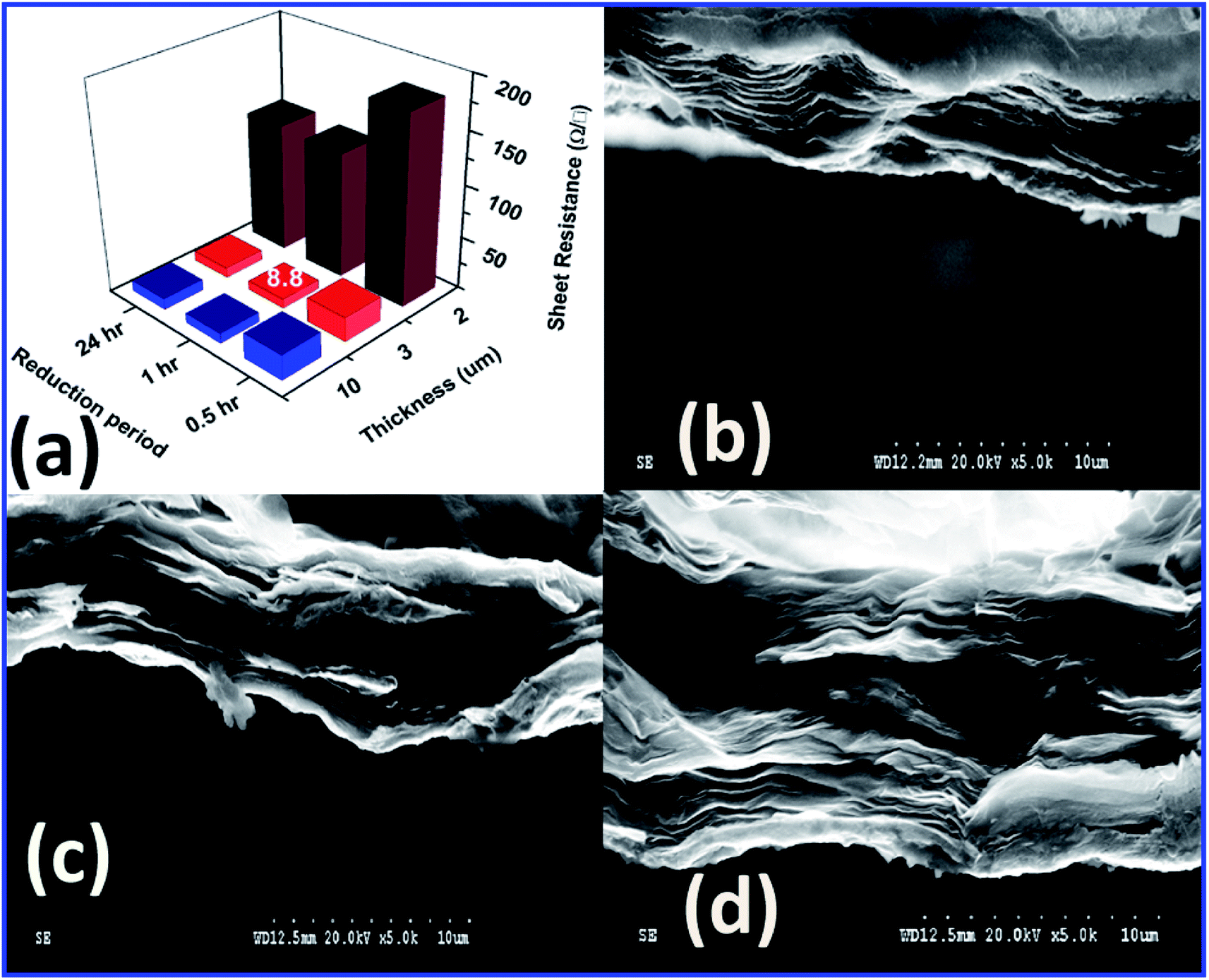 | ||
| Fig. 1 (a) Variation of sheet resistance with respect to FSG thickness and reduction period. (b, c and d) Cross sectional FESEM images of FSG with different GO concentrations (4, 8 and 10 mg mL−1, respectively) at a magnification of 5000×. | ||
However, the closest stacking of graphene sheets was observed at concentrations greater than 4 mg mL−1, indicating that the enhancement of the hydrophilic nature of GO at higher concentration results in a colloid, promoting the formation of homogeneous GO papers. The sheet resistance was measured by the four-point probe technique for all the samples as detailed in ESI.† The change in sheet resistance as a function of FSG thickness and GO precursor concentration is tabulated in Table S1.† The low Rs value of 8.8 Ω □−1 was obtained for the 3-micron-thick paper produced with a 1 h reduction process. However, changing the GO concentration to 10 mg mL−1 did not cause a great difference in the sheet resistance. Hence the concentration of 8 mg mL−1 was preferred for further characterization to explore the origin of the electrical property enhancement. The variation of electrical properties was analysed by measuring the Hall effect. Fig. 2 shows the I–V curves obtained by the van der Pauw technique, and the setup for sheet resistance measurement of the FSG samples is shown in Fig. 2(d). The electrical and Hall effect measurement methods and the related parameters are elaborated in ESI.†
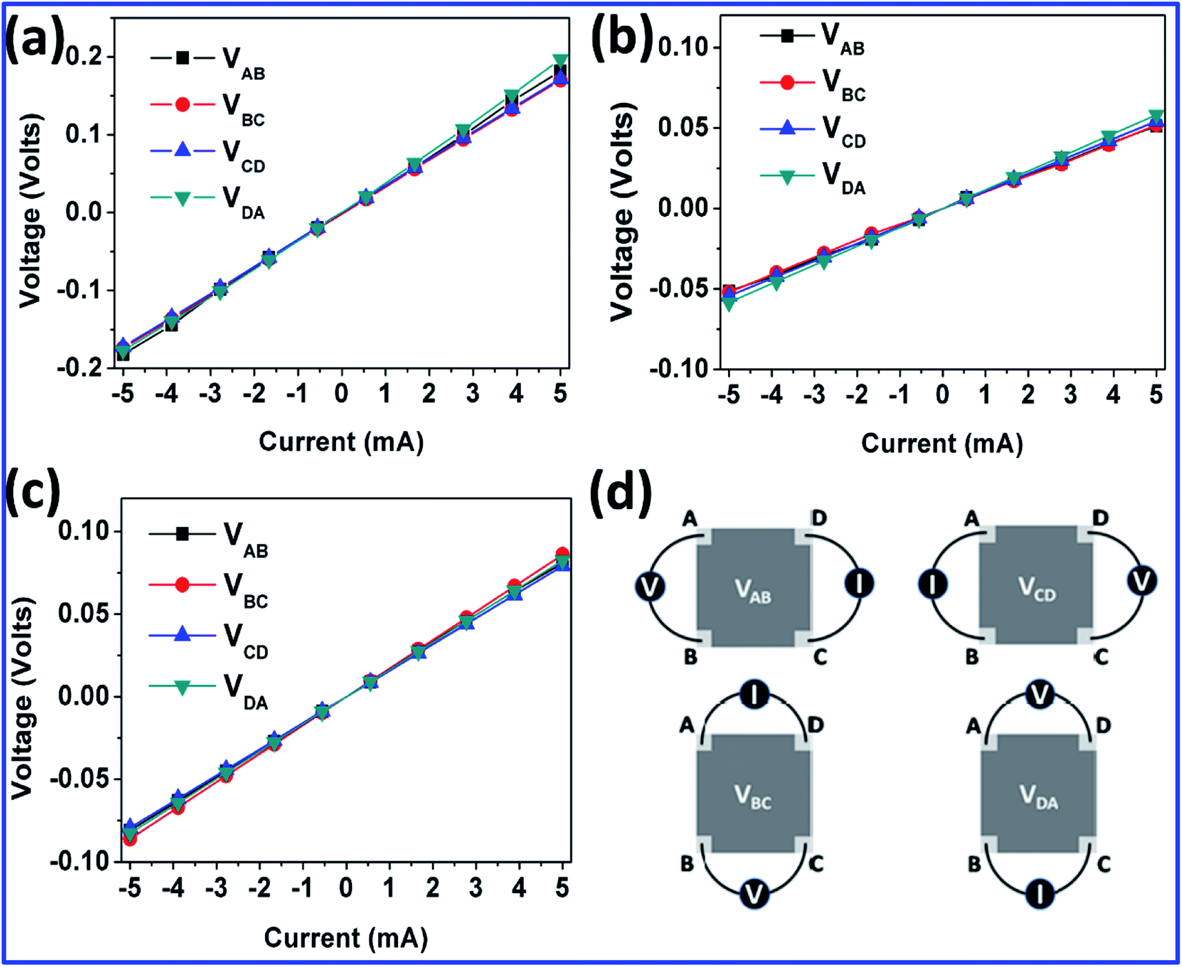 | ||
| Fig. 2 I–V curves measured by the van der Pauw method of (a) FSG1, (b) FSG2 and (c) FSG3. (d) A schematic diagram showing the measuring of electrical resistivity by the van der Pauw technique. | ||
The I–V curves show the changes in electrical resistivity for all the FSG samples obtained after different reduction times. The currents measured do not vary between the four corners, and the I–V curves are linear for all three FSG samples (FSG1, FSG2 and FSG3), as shown in Fig. 2(a, b and c). This reveals the homogeneity and uniform thicknesses of the FSG papers. Comparing the samples, the sheet resistance varies with the reduction time, and it is evident that no physical defects appear in the FSG papers when increasing the reduction time. The same FSG samples were subjected to Hall effect measurement and it was observed that these FSGs obtained by HI treatment show p-type semiconductor nature due to the highly positive value of charge in the bulk material. These electrical parameters obtained by the Hall effect will be discussed later.
3.3 Structural analysis
Deconvoluted laser Raman spectra of the D and G bands for the FSG of 3 μm thickness are shown in Fig. 3. Specifically, graphene's electronic band structure changes upon dopant interaction or when introducing impurities. The prominent peaks for graphene-based materials are the D, G and 2D bands, which imply defect sites, electron–phonon coupling of sp2 carbon and second order doubly degenerate E2g symmetry respectively.19 The electrical properties are mostly determined by the electron–phonon coupling, therefore, the G-bands of graphene-based materials are considered to be sensitive to doping effects and ion impurities. For all the FSGs with different reduction times, the G-band was relatively broad and a shoulder shift was observed on both sides. Hence the G-band was deconvoluted by the Lorentzian derivative into three peaks, namely D**, G and D′ bands, that correspond respectively to the phonon density of states, electron–phonon coupling of sp2 carbon and defective structure of sp2 carbon.19 The presence of the D′ band in all the samples might indicate the vibrational mode of iodides interacting with the graphene phonons, which broadens the G-peak. In samples FSG1 and FSG3, the D** peak due to sp3 carbon is very intense, attributed to C–I vibrations. Additionally, the improvement in electrical properties of FSG2 is manifested by the narrowing of the G-band peak, i.e. the D**/D′ intensity ratio decreases upon treating the GO paper for 1 h and hence the sheet resistance decreases. This indicates that the C–I bonds were converted into sp2 carbon in addition to the changes in the Fermi level. The 2D band is also very sensitive to doped/defect-bearing graphene. Herein, we observed the shift of the 2D band towards higher wavelength, which indicates the upward movement of the Fermi level towards positive values. This also confirms the p-type semiconductor nature of the material and is shown in Fig. S1 (ESI†).20,21 Additionally, polyiodide peaks were observed at lower wavenumbers as shown in Fig. S2† (ESI†).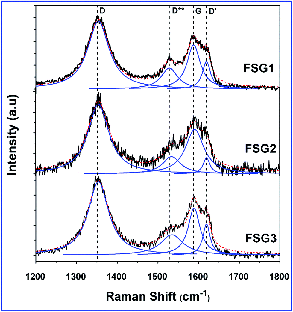 | ||
| Fig. 3 Deconvoluted laser Raman D and G bands for FSG1, FSG2 and FSG3 papers. | ||
Fig. 4(a) and (b) shows the FTIR spectra of the GO paper and FSG samples. As shown in Fig. 4(a), the content of hydroxyl groups increased from FSG1 to FSG3, which indicates the cleavage of epoxy rings to hydroxyl groups. The peaks at 1731 and 1624 cm−1 are attributed to carbonyl and hydroxyl groups of carboxylic acid moieties, respectively.22,23 They are totally absent for FSG2 and FSG3, but were found in FSG1, the sample with the highest sheet resistance. The region between 1100 and 1250 cm−1 corresponds to the epoxy groups, and was reduced in intensity after HI treatment, and the peak at 1060 cm−1 is attributed to carboxy or alkoxy functional groups, and varies between the FSG samples, which indicates the reduction of GO paper.24–26 Specifically, the peak at 1565 cm−1 that appears after HI treatment is ascribed to sp2 carbon and is strongest for FSG2, the sample for which the lowest sheet resistance was observed.27 In the XRD analysis, the GO peak of the [002] plane shifts to higher degrees, namely 24.3°, 24.4° and 24.34° for 0.5, 1 and 24 h HI-treated GO respectively. The [002] peak of FSG2 is closest to that of the graphitic plane and also the narrowest, and thus confirms the restoration of sp2 carbon for the sample.28 This indicates that 1 h treatment is sufficient for highly ordered sp2 carbon, leading to higher electrical conductivity.
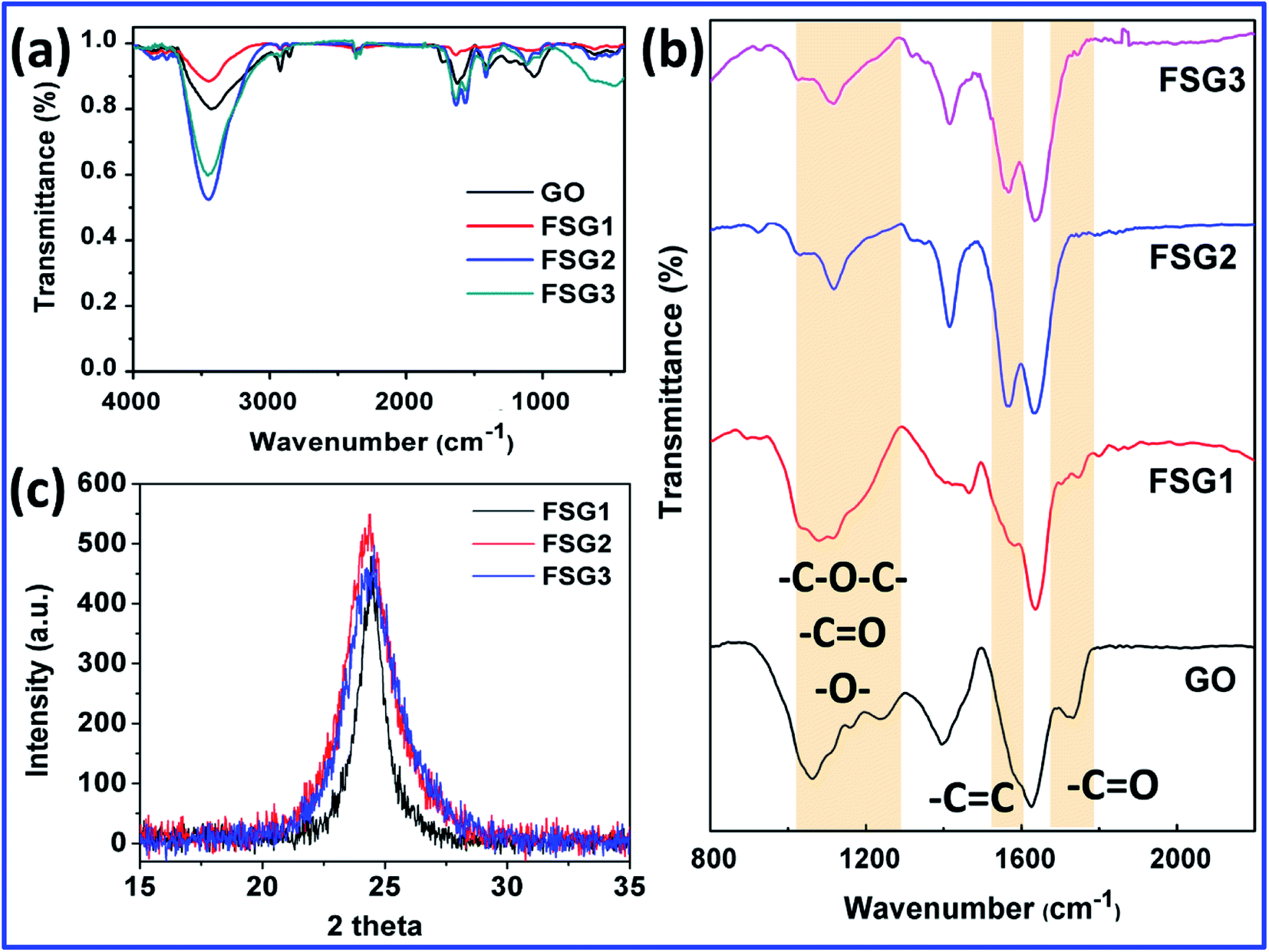 | ||
| Fig. 4 FTIR spectra of GO paper and FSG samples recorded between (a) 4000 and 500 cm−1 and (b) 2200 and 800 cm−1, and (c) XRD spectra of FSG1, FSG2 and FSG3. | ||
3.4 Factors affecting sheet resistance
From the structural analysis, it is clear that the interaction between graphene sheets and iodides dominates the electrical properties of all the samples. Raman and XRD data were extracted and correlated with the electrical properties of each sample to understand the impact of the reduction period. Table 1 shows the correlation between electrical, Raman and XRD parameters. Among the HI-treated GO papers, FSG2 shows the lowest Rs and Hall coefficient (Rh) and highest carrier density due to having the strongest interaction between graphene sheets and iodides. It is well known that Raman characterization is the best tool to analyse the effects of doping and defects in graphene. Doping of graphene sheets may occur in several ways: electrostatic doping, adsorption of impurities, substitutions or interstitials, etc., and all can be characterized by Raman spectroscopy.21 Rather than doping, however, the density and separation distance of defects dominate the quality of graphene and its electrical properties.21,29,30 Shlimak et al. observed that the defect density Nd and average distance between defects Ld, calculated using the ID/IG ratio, were directly related to the electrical properties of graphene.29 Similarly, the GO paper treated with HI solution for different periods of time was characterized by Raman spectroscopy and the Nd and Ld were calculated from the ID/IG ratio as follows:| Ld2 = 1.8 × 10⁻⁹ λL4(IG|ID) | (1) |
| Nd = 1.8 × 10²² λL−4(ID|IG) | (2) |
| Sample | Electrical parameters | Raman parameters | XRD parameters | ||||||
|---|---|---|---|---|---|---|---|---|---|
| Sheet resistance (Ω □−1) | Nc (cm−3) | Rh | Nd (cm−2) | Ld (nm) | ID/IG | [002] position | I [002] | Lc (nm) | |
| FSG1 | 120 | 4.35 × 10²⁰ | 0.014 | 3.83 × 10¹¹ | 9.17 | 1.71 | 24.30 | 430 | 13.7 |
| FSG2 | 9 | 7.70 × 10²⁰ | 0.008 | 3.47 × 10¹¹ | 9.64 | 1.55 | 24.40 | 557 | 8.5 |
| FSG3 | 19 | 5.80 × 10²⁰ | 0.010 | 3.74 × 10¹¹ | 9.28 | 1.67 | 24.38 | 497 | 8.5 |
For optimum improvement of electrical properties, the defect density should be minimized and an appropriate doping concentration should be chosen, which lead to a lower sheet resistance of graphene. However, the reduction of GO leads to higher Nd compared to pristine graphene due to the presence of fewer sp3 carbons. A low defect-density regime was found in FSG2, which provides lower sheet resistance, confirming the effective restoration of sp2 carbon as well as improvement of crystalline nature after 1 h HI treatment. From the XRD analysis, the increased intensity of the FSG2 [002] plane compared to the same plane in FSG1 and FSG3 confirms that the sp2 restoration is better in FSG2. However, iodide intercalation occurred in all the samples, increasing the sheet resistance. Further, to understand the factors affecting sheet resistance, the stacking height was calculated for all the samples as tabulated in Table 1.28,31,32 Upon reduction with HI, the stacking height (Lc) of graphene sheets decreased after 30 minutes of exposure, indicating effective reduction of GO and adsorption of fewer iodide species. However, the factors affecting electrical conductivity in FSG could not be clearly deduced from the XRD parameters.
3.5 Exploration of band gap
Fig. 5 s hows the temperature dependence of the four-point probe resistance from room temperature to 473 K.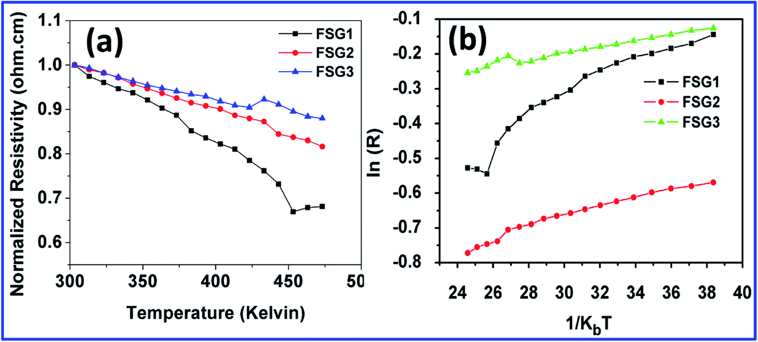 | ||
| Fig. 5 (a) Resistance vs. temperature plots of FSG samples. (b) Arrhenius plots of the temperature dependence of resistance. | ||
The four-probe setup coupled with an oven controller was utilized to analyse the temperature dependence of resistance of the FSG samples. Herein, the temperature dependence of resistance was measured in the high-temperature regime from room temperature to 473 K, where resistivity mostly depends on the band gap scattering by the phonons. Fig. 5(a) shows the normalized resistivity of the FSG samples versus temperature, indicating semiconducting behaviour for all the samples.33 The high linearity observed for FSG2 and FSG3 indicates the effect of GO reduction as well as restoration of sp2 carbon. However, from these results, it is clear that FSG2 and FSG3 have similar sheet resistances as discussed in the previous section on four-probe resistance measurement. Fig. 5(b) shows the plot of ln (R) versus T−1, which highlights the band-gap-dominated Arrhenius-like temperature dependence.34,35 The activation energy, Eg, was estimated using the temperature dependence of the conductivity for an intrinsic semiconductor.
| σ = σ0(−Eg/2KbT) | (3) |
The activation energy of the FSG samples was lower after 30 minutes reduction (14.4 meV and 9 meV for FSG2 and FSG3 respectively), which implies high conductivity at room temperature. These resistivity changes would occur due to interactions between iodide and graphene sheets. The interaction of iodides with graphene was investigated using DFT calculations and is described in ESI† (Fig. S3†).
Fig. 6 shows the Tauc plots measured for the FSG1, FSG2 and FSG3 samples. Herein, we can clearly observe that all the FSG papers have direct allowed transitions instead of indirect allowed transitions. To determine the optical band gap, the Kubelka–Munk function F(R) (a function of α, the absorption coefficient; h, Planck's constant; and ν, the light frequency) is plotted versus the photon energy of the exciting light (hν) in Fig. 6. The Kubelka–Munk function F(R) was determined from the reflectance spectra and plotted under the assumption of indirect and direct band gaps for all the samples to understand the electronic band structure. All the calculations and formulas are highlighted in the ESI.† It is well known that band opening occurs in graphene when inserting or compositing with a host material.36 Hence, the band gap of FSG is also influenced by the synergistic effect of iodides in the samples. To understand the influence of iodides interacting with graphene sheets in FSG, we have plotted both the indirect and direct transitions. Note that graphene behaves as either an indirect or direct band gap material depending on the interactions with other host materials.37–39 It may be concluded from the direct band plot that the band gap was influenced by iodide ions during the reduction of the GO papers. The band gap of FSG2 is slightly higher than those of FSG1 and FSG3 due to the strong interaction of iodides with graphene, which was also confirmed by the DFT analysis (refer to ESI†). However, the optical band gap is below 1.5 eV for all the FSG samples and is lower than that of the GO paper (Fig. S4†) after reduction with HI. Meanwhile, the energy gap obtained by the thermal studies was dominated by phonon–electron interaction, whereas the optical band gap depends upon photoexcitation. Hence, for FSG2 and FSG3, the higher activation energy and optical band gap may influence the electrical properties.
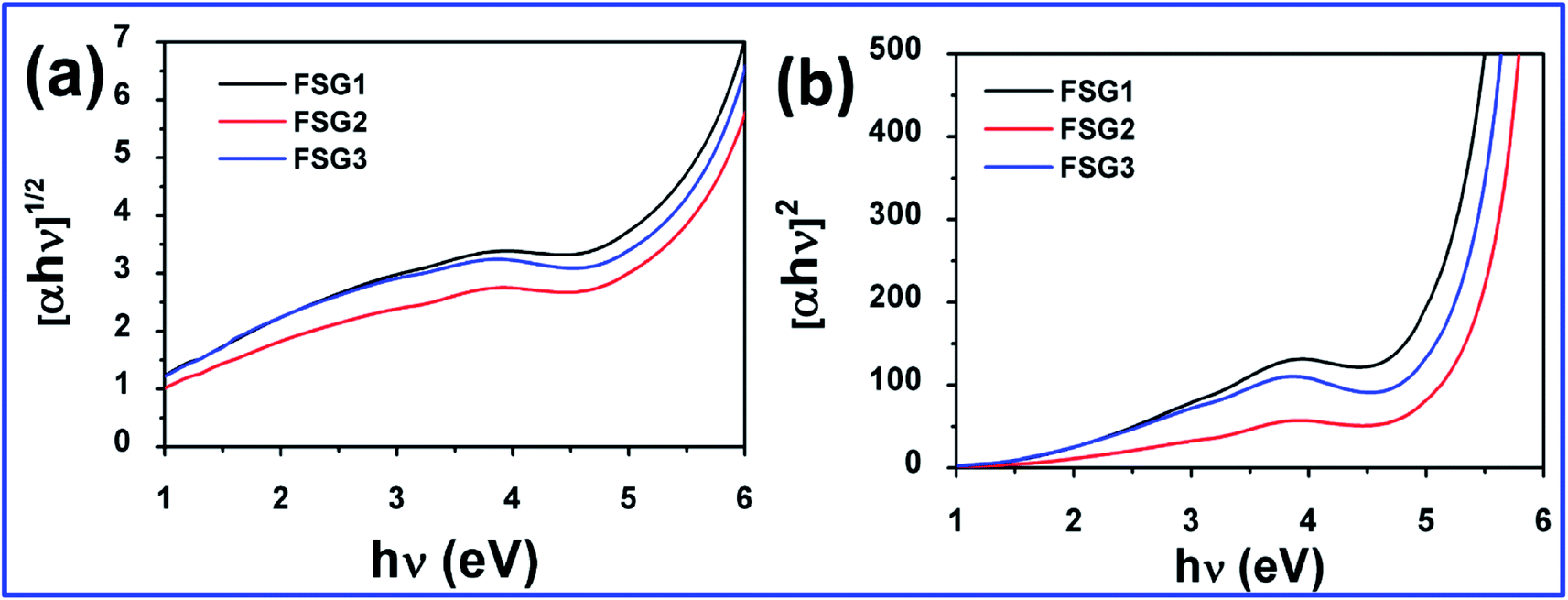 | ||
| Fig. 6 Tauc plots of FSG samples plotted with (a) indirect and (b) direct allowed transitions. | ||
4. Conclusions
In conclusion, the sheet resistance of free-standing graphene paper was influenced by the GO thickness through varying the GO concentration. It was observed that 3 micron GO thickness provided excellent sheet resistance, which was saturated thereafter. The duration of reduction treatment with HI is a significant factor affecting the electrical properties of GO paper. GO paper treated with HI for 1 h showed low sheet resistance due to a low defect density, high defect separation and a low ID/IG ratio, as confirmed by Raman investigations. An XRD study also revealed the low stacking height and highly crystalline nature of this sample (FSG2). These factors were induced by the strong interaction of iodides with graphene sheets, as confirmed by DFT analysis and other techniques. By Hall effect measurements and DFT analysis, FSG paper is concluded to be a p-type semiconductor due to the synergistic effect between graphene and iodide. The interaction of iodide with FSG was also confirmed electrochemically. Hence, we conclude that FSG electrodes obtained through HI reduction may be applied to specific devices.Conflicts of interest
There are no conflicts of interest to declare.Acknowledgements
This project was supported by South China Normal University, the outstanding young scholar project (8S0256), and the Scientific and Technological Plan of Guangdong Province (2018A050506078, 2018B050502010, 2017B090901027). This work is supported by the Project of Blue Fire Plan (No CXZJHZ201708 and CXZJHZ201709). This work was supported by the National Natural Science Foundation of China and Guangdong Province (U1601214, and 61575067). Dr M. Ramesh gratefully acknowledges the Department of Science and Technology (DST) for awarding an INSPIRE Faculty award (DST/INSPIRE/04/2015/002860).References
- G. Jo, C. Minhyeok, L. Sangchul, P. Woojin, H. K. Yung and L. Takhee, The application of graphene as electrodes in electrical and optical devices, Nanotechnology, 2012, 23, 112001–112019 CrossRef.
- B. Sukang, J. K. Sang, S. Dolly, H. A. Jong- and H. H. Byung, Towards industrial applications of graphene electrodes, Phys. Scr., 2012, T146, 014024–014031 CrossRef.
- W. Caiyun, L. Dan, O. T. Chee and G. W. Gordon, Electrochemical Properties of Graphene Paper Electrodes Used in Lithium Batteries, Chem. Mater., 2009, 21, 2604–2606 CrossRef.
- U. K. Zaheen, K. Ayesha, U. Hidayat, B. Amin and U. K. Wasid, A review of graphene oxide, graphene buckypaper, and polymer/graphene composites: Properties and fabrication techniques, J. Plast. Film Sheeting, 2016, 32, 336–379 CrossRef.
- R. Karthick and C. Fuming, Free-standing graphene paper for energy application: Progress and future scenarios, Carbon, 2019, 150, 292–310 CrossRef CAS.
- S. Ling and F. Bunshi, Mass production of graphene oxide from expanded graphite, Mater. Lett., 2013, 109, 207–210 CrossRef.
- A. D. Dmitriy, S. Sasha, J. Z. Eric, D. P. Richard, H. B. D. Geoffrey and E. Guennadi, et al., Preparation and characterization of graphene oxide paper, Nature, 2007, 448, 457–460 CrossRef.
- Z. Peng, L. Zhi, Z. Shijie and S. Guosheng, Recent Advances in Effective Reduction of Graphene Oxide for Highly Improved Performance Toward Electrochemical Energy Storage, Energy and Environmental Materials, 2018, 1, 5–12 CrossRef.
- P. Songfeng and C. Hui-Ming, The reduction of grapheneoxide, Carbon, 2012, 50, 3210–3228 CrossRef.
- R. K. Mohammad and H. Shinya, Chemical, Thermal, and Light-Driven Reduction of Graphene Oxide: Approach to Obtain Graphene and its Functional Hybrids, in Graphene Materials – Advanced Applications, ed. George ZK and Athanasios CM, IntechOpen, 2017; DOI:10.5772/67808.
- P. Songfeng, Z. Jinping, D. Jinhong, R. Wencai and C. Hui-Ming, Direct reduction of graphene oxide films into highly conductive and flexible graphene films by hydrohalic acids, Carbon, 2010, 48, 4466–4474 CrossRef.
- G. Jie, L. Chengyan, M. Lei, W. Xiaoyang and C. Yu, Free-Standing Reduced Graphene Oxide Paper with High Electrical Conductivity, J. Electron. Mater., 2016, 45, 1290–1295 CrossRef.
- L. Chenyang, H. Feng, Z. Xiaochong, Z. Qiancheng, L. Songping and L. Hong, Low temperature reduction of free-standing graphene oxide papers with metal iodides for ultrahigh bulk conductivity, Sci. Rep., 2014, 4, 3965 Search PubMed.
- R. Karthick, M. Brindha, M. Selvaraj and S. Ramu, Stable colloidal dispersion of functionalized reduced graphene oxide in aqueous medium for transparent conductive film, J. Colloid Interface Sci., 2013, 406, 69–74 CrossRef CAS.
- C. K. Chua and P. Martin, Chemical reduction of graphene oxide: a synthetic chemistry viewpoint, Chem. Soc. Rev., 2014, 43, 291–312 RSC.
- K. M. In, L. Junghyun, S. R. Rodney and L. Hyoyoung, Reduced graphene oxide by chemical graphitization, Nat. Commun., 2010, 1, 73 CrossRef PubMed.
- A. H. Robert, E. Marielle R, D. C. Ekin, D. V. Chad and K. Efthimios, Polyiodide-Doped Graphene, J. Phys. Chem. C, 2017, 121(1), 609–615 CrossRef.
- T. Damien, P. Pascal and C. G. Iann, Theoretical study of polyiodide formation and stability on monolayer and bilayer graphene, Phys. Chem. Chem. Phys., 2015, 17, 30045–30051 RSC.
- A. Kaniyoor and S. Ramaprabhu, A Raman spectroscopic investigation of graphite oxide derived graphene, AIP Adv., 2012, 2, 032183 CrossRef.
- L. Jisook, S. N. Konstantin and S. S. Hyeon, Interaction between Metal and Graphene: Dependence on the Layer Number of Graphene, ACS Nano, 2011, 5(1), 608–612 CrossRef PubMed.
- B. Ryan, G. C. Luiz and N. Lukas, Raman characterization of defects and dopants in graphene, J. Phys. Condens. Matter, 2015, 15, 083002 Search PubMed.
- S. Stankovich, R. D. Piner, S. T. Nguyen and R. S. Ruoff, Synthesis and Exfoliation of Isocyanate-Treated Graphene Oxide Nanoplatelets, Carbon, 2006, 44, 3342–3347 CrossRef CAS.
- L. Shahriary and A. A. Athawale, Graphene Oxide Synthesized by Using Modified Hummers Approach, Int. J. Electr. Electron. Eng., 2014, 2(1), 58–63 Search PubMed.
- L. F. Dumeea, C. Fenga, L. Hea, F. M. Alliouxa, Z. Yia and W. Gaoa, et al., Tuning the Grade of Graphene: Gamma Ray Irradiation of Free-Standing graphene Oxide Films in Gaseous Phase, Appl. Surf. Sci., 2014, 322, 126–135 CrossRef.
- Y. Y. Dou, M. Luo, S. Liang, X. L. Zhang, X. Y. Ding and B. Liang, Flexible Free-Standing Graphene-Like Film Electrode for Supercapacitors by Electrophoretic Deposition and Electrochemical Reduction, Trans. Nonferrous Metals Soc. China, 2014, 24, 1425–1433 CrossRef CAS.
- R. J. Seresht, M. Jahanshahi, A. M. Rashidi and A. A. Ghoreyshi, Synthesis and Characterization of Thermally-Reduced Graphene, Iran. J. Energy Environ., 2013, 4(1), 53–59 Search PubMed.
- A. C. Obreja, D. Cristea, R. Gavrila, V. Schiopu, A. Dinescu and M. Danila, et al., Isocyanate Functionalized Graphene/P3HT Based Nanocomposites, Appl. Surf. Sci., 2013, 276, 458–467 CrossRef CAS.
- B. Manoj and A. G. Kunjomana, Study of Stacking Structure of Amorphous Carbon by X-Ray Diffraction Technique, Int. J. Electrochem. Sci., 2017, 7, 3127–3134 Search PubMed.
- Z. Rong, J. Ruwantha, S. Andriy, D. Ruchira, A. Meysam and B. J. Jacek, et al., In Situ Transport Measurements and Band Gap Formation of Fluorinated Graphene, J. Phys. Chem. C, 2015, 119, 20150–20155 CrossRef.
- M. Trushin, Thermally activated conductivity in gapped bilayer graphene, Europhys. Lett., 2012, 98, 47007 CrossRef.
- S. Burcu, D. Fatma and Y. Yuda, Utilization of multiple graphenenanosheets in fuel cells: 2. The effect of oxidation process on the characteristics of graphenenanosheets, Fuel, 2011, 90, 2609–2616 CrossRef.
- A. Beti, G. Anita, P. Perica and T. D. Aleksandar, X-ray diffraction analysis on layers in graphene samples obtained by electrolysis in molten salts: a new perspective, Micro Nano Lett., 2015, 10, 683–685 CrossRef.
- A. B. Richard and H. W. David, The Dependence of Resistance on Temperature for Metals, Semiconductors, and Superconductors, J. Chem. Educ., 1997, 74(9), 1090 CrossRef.
- E. Goki, M. Cecilia, Y. Hisato, K. HoKwon and C. Manish, Insulator to Semimetal Transition in Graphene Oxide, J. Phys. Chem. C, 2009, 113(35), 15768–15771 CrossRef.
- C. Lijie, S. Li, J. Chuanhong, J. Deep, W. Dangxin and L. Yongjie, et al., Atomic layers of hybridized boron nitride and graphene domains, Nat. Mater., 2010, 9, 430–435 CrossRef.
- M. M. MonshiS, M. Aghaei and I. Calizo, Band gap opening and optical absorption enhancement in graphene using ZnOnanocluster, Phys. Lett. A, 2018, 382, 1171–1175 CrossRef.
- A. M. Ismail, M. I. Mohammed and S. S. Fouad, Optical and structural properties of polyvinylidene fluoride (PVDF)/reduced graphene oxide (RGO) nanocomposites, J. Mol. Struct., 2018, 1170, 51–59 CrossRef CAS.
- S. L. Joseph, A. O. John, F. K. Mugwanga and G. G. Katana, Tuning the Band Gap Energy of Reduced GrapheneOxide Using Biopolymer Chitosan for High Powerand Frequency Device Applications, Am. J. Polym. Sci. Eng., 2019, 7, 8–19 CAS.
- M. A. Velasco-Sotoa, S. A. Pérez-Garcíaab, J. Alvarez-Quintanaab, Y. C. L. Nyborgc and L. Licea-Jiménez, Selective band gap manipulation of graphene oxide by its reduction with mild reagents, Carbon, 2015, 93, 967–973 CrossRef.
Footnote |
| † Electronic supplementary information (ESI) available. See DOI: 10.1039/c9ra05529k |
| This journal is © The Royal Society of Chemistry 2019 |