
 Open Access Article
 This Open Access Article is licensed under a Creative Commons Attribution-Non Commercial 3.0 Unported Licence
Beneficial effects of potassium iodide incorporation on grain boundaries and interfaces of perovskite solar cells†
Yin Yanga,
Lili Wu*ab,
Xia Hao *b,
Zeguo Tangc,
Huagui Laia,
Jingquan Zhangab,
Wenwu Wanga and
Lianghuan Fenga
*b,
Zeguo Tangc,
Huagui Laia,
Jingquan Zhangab,
Wenwu Wanga and
Lianghuan Fenga
aInstitute of Solar Energy Materials and Devices, College of Materials Science and Engineering, Sichuan University, Chengdu 610064, China. E-mail: wulili@scu.edu.cn; hao.xia0808@scu.edu.cn; Fax: +86 28 85412542; Tel: +86 28 85412542
bInstitute of New Energy and Low-Carbon Technology, Sichuan University, Chengdu 610027, China
cChengdu Research Center, Hanergy Thin Film Power Group Ltd., Chengdu 610200, China
First published on 10th September 2019
Abstract
Grain boundaries and interfacial impurities are the main factors that limit the further development of polycrystalline perovskite solar cells because their existence severely deteriorates the device performance. In order to optimize the efficiency of perovskite solar cells, it is essential to eliminate these defects. In the present work, potassium iodide (KI) is incorporated into the perovskite absorber. KI incorporation improves the crystallinity of the perovskite, increases the grain size, and decreases the contact potential distribution at the grain boundary, which are verified by X-ray diffraction, scanning electronic microscopy and Kelvin probe force microscopy. Besides, the activation energy of the recombination, estimated from the temperature dependent current–voltage of perovskite solar cells, is larger than the bandgap calculated from the temperature coefficient. These suggest that KI incorporation effectively passivates the grain boundaries and interfacial defects. As a result, charge trapping in the absorber as well as the bimolecular and trap-assisted recombination of the device are significantly suppressed. Consequently, the open circuit voltage and fill factor of the incorporated devices are greatly improved, enabling an optimized power conversion efficiency of 19.5%, in comparison with that of 17.3% for the control one. Our work provides an effective strategy of defect passivation in perovskite solar cells by KI incorporation and clarifies the mechanism of the performance optimization of KI incorporated devices.
Introduction
Over the past decade, the efficiency of organic–inorganic halide hybrid perovskite solar cells has increased from 3.8% to over 24%. Such rapid development has made them a strong competitor in the thin film solar cell community.1 One of the most important reasons for the wide investigation of perovskite solar cells is the advantages of the organic–inorganic halide hybrid perovskite material, such as long lifetime and diffusion length of the carrier,2–4 the tuneable band gap.5 Besides, the inexpensive raw materials and simple preparation processes make it possible to achieve large-scale and cost-effective production.The common structure of the organic–inorganic halide hybrid perovskite material is AMX3 (A = methylammonium (MA) CH3NH3+, or formamidinium (FA) CH3(NH2)2+; M = Pb2+ or Sn2+; X = Cl−, Br− or I−). The solution-processable spin coating is one of the regular techniques for preparing absorber and other functional layers of perovskite solar cells. However, impurities at the grain boundaries (GBs) and interfacial defects are inevitable. Although GBs are not acting as recombination centres, they severely hinder the lateral diffusion of carriers and as a result, degrade the device performance.6 Thus, there have been many reports attempting to modify GBs by incorporating various additives into the absorption layer of perovskite solar cells to achieve improvements both in efficiency and in stability. A passivation functional groups contained carboxyl, amine groups and aromatic structures were customized by Yang et al., and the loss of open circuit voltage for the perovskite solar cell was reduced due to the successful elimination of defects in the absorption layer.7 Niu et al. demonstrated that the trap states near the GB can be effectively passivated by semiconductor molecules having Lewis acid functional groups.8 In addition, interfacial defects are generated during the fabrication process of a sandwich-structured perovskite solar cells, they deteriorate the device performance due to the increased trap-assisted recombination probabilities and recombination velocities. The possible strategy could be modifying the contact properties between the perovskite layer and functional layers by incorporating additives into absorber. Lee et al. added phenethyl ammonium to the absorption layer to form a quasi-two-dimensional material with a large band gap at the interface, which provided effective interface passivation and an optimized device performance was witnessed.9
Alkali metals such as K,10,11 Rb12,13 and Cs14,15 with small ionic radii are often used to replace part of the A-site organic ion of the perovskite structure and the incorporation of alkali metals into perovskites has been proved to be beneficial to suppress the hysteresis effect and improve the stability of perovskite solar cells. It has been confirmed that the incorporating of KI will improve the overall performance of perovskite solar cells. The results of Tang et al. suggested that the band alignment of the perovskite could be modified by KI incorporation, and the electron transport barrier was then reduced. The hysteresis effect was therefore eliminated.11 Bu et al. found that KI could eliminated hysteresis by enhancing conductivity which accelerated the charge transport and distribution.16
In our work, we investigated the effects of the defects at GBs and interfaces from the point view of charge transportation and recombination. We found that KI incorporation realized an obvious increase in PCE of perovskite solar cells and the shelf lifetime τ80 of the unencapsulated devices increased from less than 200 hours to over 1000 hours. The Kelvin probe force microscopy (KPFM), steady state/time-resolved photoluminescence (PL) and temperature-dependent current density–voltage (JVT) measurements were carried out to clarify the mechanism of performance improvement induced by KI incorporation. The results suggest that the main reason of these improvements is the effective GB and interface passivation, which decrease the barrier of charge transport at the GBs of perovskites and suppress the bimolecular and trap-assisted recombination of the solar cells. This verifies the importance of GB and interface passivation for optimizing both the power conversion efficiency and the long-term stability of perovskite solar cells.
Experiment
Device fabrication
The structure of the perovskite solar cells in this work is glass/FTO/SnO2/compact-TiO2/mesoporous-TiO2/(FA0.83MA0.17)Pb(I0.83Br0.17)3/spiro-OMeTAD/Au. The FTO-coated glass substrates (NSG TEC 12D, with a 12 Ω □−1 square resistance) were purchased from Pilkington Group Limited and a 30 nm-thick SnO2 was then sputtered. The substrates were cleaned in sequence in an ultrasonic bath with Amway, deionized water and ethanol. After being dried with N2, the substrates were finally treated by UV-ozone for 15 minutes. The titanium diisopropoxide diluted in absolute ethanol was used to prepare the compact-TiO2 (c-TiO2) by spray pyrolysis with N2 as a carrier gas on a hot plate at 400 °C. A mesoporous TiO2 (mp-TiO2) layer was then deposited by spin coating for 40 s at 4000 rpm with a ramp of 2000 rpm s−1 to achieve a 150–200 nm-thick layer, using a TiO2 particle paste (Dyesol 30 NR-D) diluted in ethanol.The (FA0.83MA0.17)Pb(I0.83Br0.17)3 film was formed by one-step spin coating of the mixed perovskite precursor solution. The composition of the perovskite precursor solution was FAI (1 M), PbI2 (1.05 M), MABr (0.2 M) and PbBr2 (0.2 M) in a mixed solvent of anhydrous N,N-dimethylformamide (DMF) and dimethyl sulfoxide (DMSO). The KI incorporated perovskites were obtained by adding 1.5 M–KI solution into precursors without introducing any other chemicals.
To deposit a perovskite film, the perovskite precursor solution was transferred to an N2 glove box with a relative humidity less than 10%, and then dropped onto the TiO2-coated FTO substrate. The substrate was spun at 1000 rpm and 4000 rpm for 10 s and 50 s respectively. 300 μL of chlorobenzene was poured on the substrate 10 s prior to the end of the program. The as-spun perovskite film was then annealed on a hot plate at 160 °C for 15 minutes. The hole transport layer was spin-coated on the surface of perovskite layer at 3000 rpm for 30 s by dropping a solution of spiro-OMeTAD in chlorobenzene (72.3 mg/1 mL) incorporated by lithium bis(trifluoromethylsulphonyl)imide (Li-TFSI, Sigma-Aldrich) and 4-tert-butylpyridine (TBP, Sigma-Aldrich). Finally, a 100 nm-thick Au electrode was thermally evaporated via a shadow mask and the full structure of the solar cell with a typical area of 0.1886 cm2 was completed.
Characterization
The X-Ray Diffraction (XRD) was performed on a DX-2600 X-ray diffractometer (Dandong Fangyuan Instrument Company) with Cu-Kα radiation (scan range from 10° to 70°). The morphology of the film was observed by a field emission scanning electron microscope (Hitachi S-4300). KPFM measurement was performed on the surface of the perovskite films in ambient air condition, using Multi Mode 8 AFM with commercially available MESP conductive probe coated with Co/Cr. KPFM is used to study the spatially resolved imaging of surface contact potential difference (CPD). The photovoltaic characteristics were measured using a Keithley 2400 Source Meter under simulated AM 1.5G sunlight (Sun 2000 solar simulator, ABET Technology) with an illumination power density of 100 mA cm−2, which is calibrated by a GaAs standard cell. The JVT characteristics of solar cells were carried out under a simulated AM1.5 sunlight. The light-induced temperature gradient on the sample was negligible and the temperature was increased from 300 K to 360 K with a step of 5 K. The device was heated by a self-made resistance heater and the temperature was monitored by a bonded thermocouple (ST-50, PKC, Inc.). The steady state photoluminescence (PL) and time-resolved photoluminescence (TRPL) of perovskite films were characterized by the Edinburgh Instruments FLS 980 fluorescence spectrometer.Results and discussion
The cell structure is glass/FTO/SnO2/c-TiO2/mp-TiO2/K(FA0.83MA0.17)Pb(I0.83Br0.17)3/spiro-OMeTAD/Au. The volume ratio of KI is set as 0% [K0(FA0.83MA0.17)Pb(I0.83Br0.17)3], 3% [K0.03(FA0.83MA0.17)0.97Pb(I0.83Br0.17)3] and 6% [K0.06(FA0.83MA0.17)0.94Pb(I0.83Br0.17)3], which are marked as control, 3% K+ and 6% K+ respectively (the volume ratio is defined as MKI/MKI + MFA + MMA). The photovoltaic parameters are obtained from 10 units cell of each batch, as shown in Fig. 1. Best performance is achieved when the molar ratio of KI is 3% and the average parameters are: short circuit current density (Jsc) = 24.67 mA cm−2, open circuit voltage (Voc) = 1.07 eV, fill factor (FF) = 72.86%, power conversion efficiency (PCE) = 19.27%.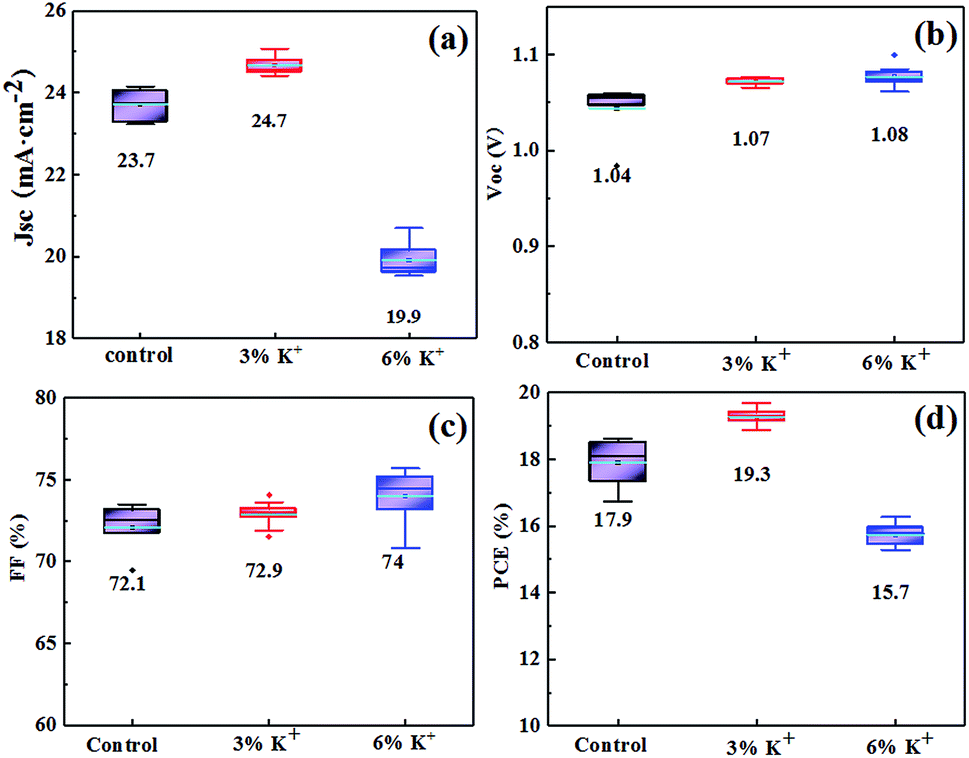 | ||
| Fig. 1 The box charts of performance parameters: (a) Jsc, (b) Voc, (c) FF and (d) PCE for perovskite solar cells with different incorporating concentrations. | ||
The short-circuit current density decreased when we kept increasing the volume ratio of KI to 6%. It has been clarified that this performance deterioration was mainly due to the lattice constant mismatch caused by K+ with a small ionic radius (1.33 Å). It is kinetically unfavourable for films crystallization to produce a preferred face orientation.17 Therefore, in this study, we chose 3% as the incorporating concentration of KI for further investigation.
The morphologies of the perovskite films are shown in Fig. 2. After KI incorporation, the grain size of the film is obviously increased, as shown in Fig. 2a and c. One may find in Fig. 2e that after KI incorporation, the average grain size increased from 0.64 to 1.07 μm, and half of grains grew to over 1 μm. Therefore, the GBs were significantly reduced after KI incorporation, which can effectively suppress the effect of ion diffusion between the functional layers of the device. It is worth noting that in Fig. 2b and d, the large grains are perpendicular to the substrate, which suggests that here only the vertical GBs are formed. Therefore, in case of the KI incorporated devices, the vertical GBs decreased, and no extra lateral GBs were introduced. Therefore, the charge trapping interfaces and photocurrent conduction paths in the KI incorporated devices will be effectively decreased.18 Besides, by investigating series of SEM images for control and K+ incorporated perovskite films, we found that after KI incorporation, small particles were emerged at the GBs, as observed in Fig. 2c. It has been confirmed that these particles are PbI2. Their results also suggest that the existence of PbI2 could suppress charge carrier recombination and improve the Voc of perovskite solar cells.19,20 Furthermore, because of the shorter Pb–I bond length and higher bond strength, the PbI2 solubility in water is lower. As compared with perovskite, PbI2 on the surface of perovskite film is more resistant to moisture-induced degradation.21 And as a result, the water induced degradation of the perovskite solar cells will be suppressed after KI incorporation.
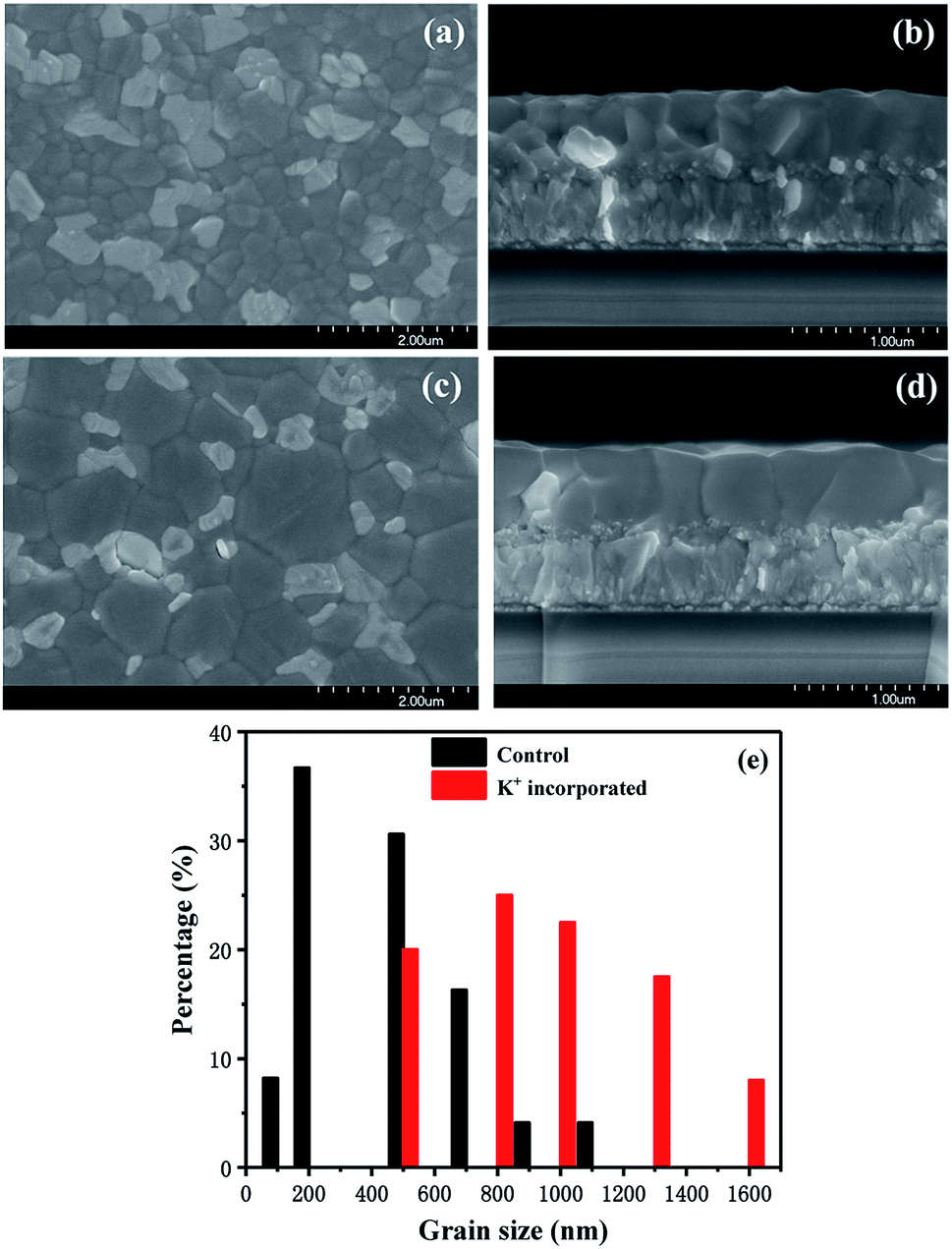 | ||
| Fig. 2 Surface and cross-sectional morphologies of (a and b) control and (c and d) K+ incorporated perovskite films. (e) Grain size distribution corresponding to SEM images. | ||
The crystallinity of the perovskites was analysed by XRD and the results are shown in Fig. 3. The red curve (a) and the black curve (b) represent the crystal structure of the KI incorporated and control films, respectively. It is found that both mixed perovskite films show a perovskite phase (α-phase), rather than a non-perovskite phase (δ-phase), regardless of the of the incorporating ions. This is consistent with the observation in other works.22,23 The main peaks at 14.04°, 19.94°, 24.52°, 28.3°, 31.74° and 40.51° are assigned to the (001), (011), (111), (002), (012) and (022) crystal planes. Peaks marked by # and * are the diffraction peaks of the PbI2 and the substrate. After KI incorporation, the PbI2 peak is obviously suppressed, which indicates that more perovskite phase is formed. Meanwhile, the apparent enhancement of the peaks of (001) and (002) suggests good crystallinity of the tetragonal phase perovskite after incorporating.17 The better crystallinity suggests fewer defects in KI incorporated perovskite film.
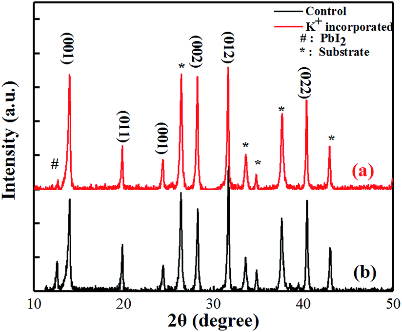 | ||
| Fig. 3 XRD patterns of (a) K+ incorporated and (b) control perovskite films. | ||
The KPFM was performed to measure the contact potential difference (CPD) on the surface of the film to further verify the effect of KI incorporation on GBs. The sample structure for KPFM measurement was glass/FTO/SnO2/c-TiO2/mp-TiO2/perovskite. KPFM is a derivative based on atomic force microscopy with high resolution (<10 nm), which can get the surface topography and CPD images simultaneously, quantify local charge generation and separation within the film. The KPFM can provide a feasible approach to identify grain interiors and GBs. Fig. 4 shows the topographic images of perovskites and the corresponding KPFM results over the surface of the samples. Fig. 4a and c are the surface morphology of the perovskites and one may find that after K+ incorporating, the grain size of perovskite is significantly increased, which is consistent with the SEM images. Moreover, Fig. 4a and c show that the arithmetic mean roughness (Ra) and root mean square roughness (Rq) of the film incorporated with K+ are 20.4 nm and 26.0 nm respectively, which are both smaller than that of the control film (27.5 nm and 34.8 nm, respectively). This suggests that KI incorporation effectively modifies and smoothens the surface of the perovskite. This might be contributing to the performance improvement of the corresponding devices.
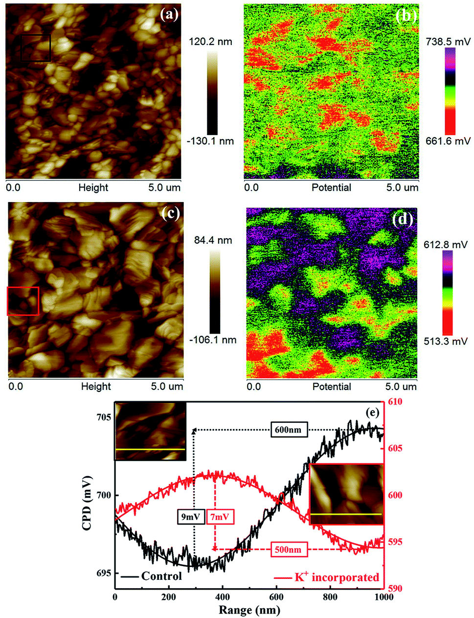 | ||
| Fig. 4 Atomic force microscopy (AFM) and contact potential difference (CPD) images of (a and b) control and (c and d) incorporated perovskite films. (e) CPD distribution of control and K+ incorporated samples across the GBs in black and red squares in (a) and (c). | ||
Fig. 4b and d show the KPFM results over the surface of the perovskites, which are obtained at the same time while measuring the surface morphology. As shown in Fig. 4a, the grain size is small, and the GBs of the control sample are not clear. And as a result, the change of CPD in Fig. 4b is not obvious. On the contrary, in case of KI incorporated sample, as shown in Fig. 4c, a significant increase in the grain size could be observed, which makes the GBs clearly visible. One may notice that the CPD at the GBs in Fig. 4d is smaller than that at the grain interiors. The possible reason of the decreased CPD could be the increased built-in potential that induced by the interstitial or vacancy defects at the GBs. It has been confirmed that the defects at GBs are mainly associated with iodine in perovskites. With the presence of K+, the iodine atoms are partially replaced by bromine, immobile KBr compounds would be generated. The charge trapping induced by the defect states at the GBs will then be eliminated.24 In Fig. 4e, we plotted the CPD distribution of GBs corresponding to the black and red squares in Fig. 4a and c and we found that both of them consistently show the Gaussian distribution (the two yellow lines in Fig. 4e are the specific locations selected). The barrier of the carrier crossing the GB is reflected by the trough value, and the full width at half maximum (FWHM) value of the plot can be attributed to the depletion range of the GB.25 From Fig. 4e, we can see that after KI incorporation, the trough value reduced from 9 mV to 7 mV and FWHM reduced from 600 nm to 500 nm. After KI incorporation, the depletion region of the GB is narrowed and the barrier height for the carriers to transport across the GB is reduced, which ensure efficient transportation of charge carriers.
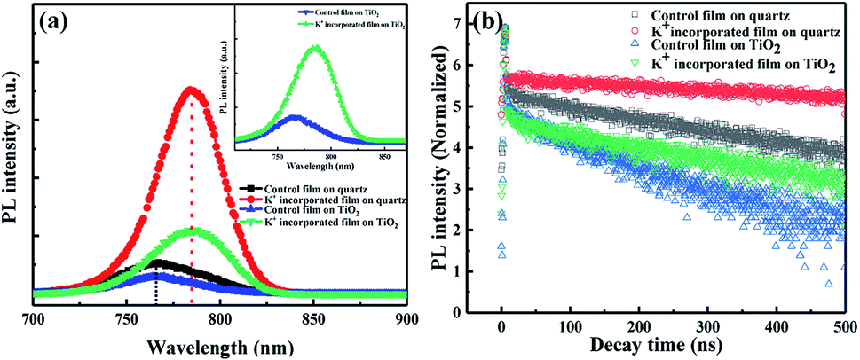
Fig. 5 displays the steady state photoluminescence (PL) and time-resolved photoluminescence (TRPL) spectra of perovskite films. According to the PL spectra, the relative intensities of the photo-generated carrier radiation recombination and non-radiative recombination in the film can be intuitively understood.26 In order to exclude the effect of the electron transport layer on the test results, we also measured PL and TRPL of the perovskites deposited on bare glass substrates marked as control/K+ incorporated film on quartz. After KI incorporation, the band gap (Eg) of the perovskite decreases from 1.62 eV to 1.61 eV due to the small ionic radius of K+. As shown in Fig. 5a, the KI-incorporated film exhibits stronger PL peak intensity whether it contains an electron transport layer (ETL) or not (the inset of Fig. 5a is the PL patterns of perovskites deposited on TiO2). For the film deposited on glass substrate, the PL intensity of KI incorporated (red) sample is ten times stronger than that of control one (black), which indicates that the incorporation of KI greatly inhibits non-radiative trap-assisted recombination due to the reduced internal defect states in perovskite thin films.
 | ||
| Fig. 5 (a) Steady state photoluminescence and (b) time resolved photoluminescence charts of perovskite films. | ||
The charge carrier recombination was then further studied by using TRPL. The PL decay curves of the perovskites are shown in Fig. 5b and the derived lifetimes are summarized in Table 1. The decay curve is fitted by a double exponential function model: IPL(t) = A + B1![[thin space (1/6-em)]](https://www.rsc.org/images/entities/char_2009.gif) exp(−t/τ1) + B2exp(−t/τ2), where t is time, IPL(t) is the time-dependent PL strength, and B1/B2 is the amplitude of the attenuation component τ1/τ2.27 It contains a fast decay (τ1) and a slow decay process (τ2). For perovskites, the τ1 indicates surface recombination and it is generally believed to be not obviously correlated with the device performance. Therefore, we will not discuss about it in details.9,28 On the contrary, τ2 is considered as the radiation recombination in bulk of perovskite before the free carriers are collected.29 In Fig. 5b, the red and black curves are TRPL of incorporated and control perovskite films directly deposited on quartz glass, revealing that τ2 increases from 281.9 to 1186 ns after KI incorporation. This suggests effective suppression of the recombination induced by defect states in the KI incorporated perovskite film. The elimination of the trap states in the perovskite after KI incorporation is ascribed to the occupation of the halide vacancy defects by the excess I−.30 At the same time, τ1 and τ2 in both perovskites deposited on ETL coated substrates before and after KI incorporation are decreased in comparison with that deposited on bare glass. This reflects efficient transport of electrons from the perovskite layer to the ETL. It is worth noting that though the lifetime of incorporated one (239.6 ns) is still higher than the control (123.8 ns), it reduced a lot compared to the original lifetime without ETL. Which not only indicates the lower defect concentration of the film itself, but also suggests an improved charge transport capability at the interface of absorber/ETL after incorporating.
exp(−t/τ1) + B2exp(−t/τ2), where t is time, IPL(t) is the time-dependent PL strength, and B1/B2 is the amplitude of the attenuation component τ1/τ2.27 It contains a fast decay (τ1) and a slow decay process (τ2). For perovskites, the τ1 indicates surface recombination and it is generally believed to be not obviously correlated with the device performance. Therefore, we will not discuss about it in details.9,28 On the contrary, τ2 is considered as the radiation recombination in bulk of perovskite before the free carriers are collected.29 In Fig. 5b, the red and black curves are TRPL of incorporated and control perovskite films directly deposited on quartz glass, revealing that τ2 increases from 281.9 to 1186 ns after KI incorporation. This suggests effective suppression of the recombination induced by defect states in the KI incorporated perovskite film. The elimination of the trap states in the perovskite after KI incorporation is ascribed to the occupation of the halide vacancy defects by the excess I−.30 At the same time, τ1 and τ2 in both perovskites deposited on ETL coated substrates before and after KI incorporation are decreased in comparison with that deposited on bare glass. This reflects efficient transport of electrons from the perovskite layer to the ETL. It is worth noting that though the lifetime of incorporated one (239.6 ns) is still higher than the control (123.8 ns), it reduced a lot compared to the original lifetime without ETL. Which not only indicates the lower defect concentration of the film itself, but also suggests an improved charge transport capability at the interface of absorber/ETL after incorporating.
| Eg (eV) | τ1 (ns) | τ2 (ns) | |
|---|---|---|---|
| Control film on quartz | 1.62 | 0.875 | 281.9 |
| K+ incorporated film on quartz | 1.58 | 0.957 | 1186 |
| Control film on TiO2 | 1.62 | 0.509 | 123.8 |
| K+ incorporated film on TiO2 | 1.58 | 0.752 | 239.6 |
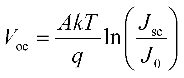
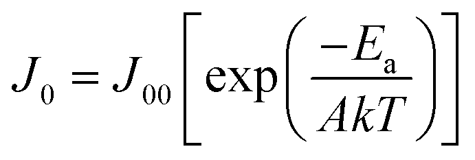
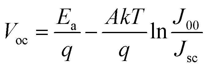
The recombination mechanism of perovskite solar cells was then investigated by using temperature-dependent current–voltage (JVT) measurement. Fig. 6a and b show the fitted line of Voc as a function of T during heating and cooling processes, respectively. By fitting the J–V curves with the ideal diode eqn (1) and J0 can be expressed as eqn (2). According to the activation energy determined from the Voc–temperature (Voc–T) curve by the eqn (3):
 | (1) |
 | (2) |
 | (3) |
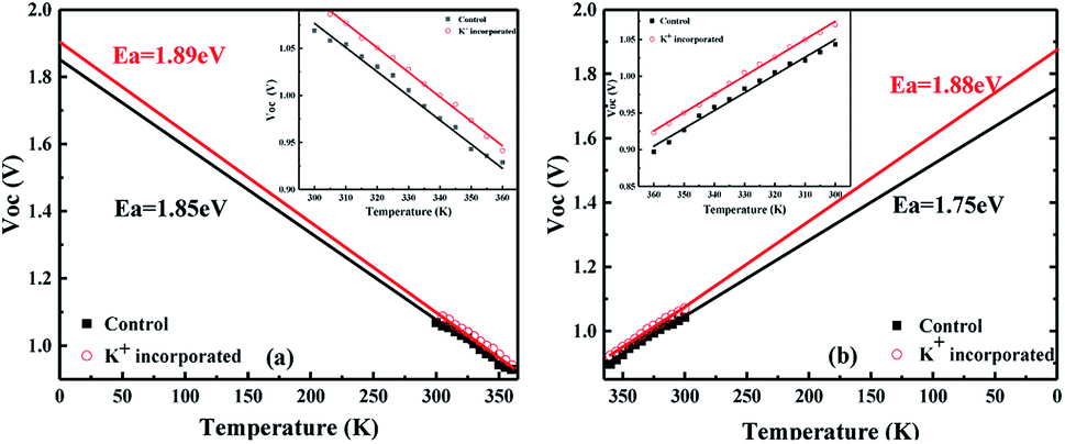 | ||
| Fig. 6 Temperature-dependent current–voltage image (Voc–T) of devices at AM1.5, the solid lines are the linear fitting of the measured points. (a) and (b) are the heating and cooling processes, respectively. | ||
We measured the temperature dependent light J–V of the devices in a temperature cycle of 300–360–300 K. The results of the heating and cooling processes for both devices are shown in Fig. 6. In heating process, the Voc are linearly correlated with temperature. In both devices, Voc follows a straight line for temperature and the extrapolation of the activation energy is higher than the Eg of the perovskite calculated according to the temperature coefficient. Furthermore, the activation energy of the device after incorporating KI (1.89 eV) is greater than that of control one (1.85 eV). These indicate that there are fewer defects inside the incorporated perovskite film, better contact with the functional layers and the internal recombination of carriers is much larger than the interfacial recombination.31 All of the aforementioned factors contribute to the improved device performance. Fig. 6b shows the temperature dependent Voc when the sample is cooled down from 360 K to 300 K. It can be found that the Voc of the cell incorporated with KI can be normally restored to the original state, and thus the derived activation energy is hardly changed. However, on the contrary, the Voc of the control device cannot be restored to the initial state with a reduced activation energy from 1.85 eV to 1.75 eV. This is attributed to the fact that incorporating KI not only reduces the interfacial recombination, but also improves the thermal stability of the cell. As can be seen in Fig. S3,† we have performed the temperature-dependent IV measurements on over 5 sets of control/incorporated perovskite solar cells and found that results were well reproducible. The activation energies of the incorporated samples were between 1.89–1.96 eV, and those of the control ones were between 1.82–1.87 eV.
Fig. 7 is the forward and reverse scan of the J–V curves for specific devices which possess the photovoltaic parameters (summarized in Table 2) close to the average values of each batch. From Fig. 7 and Table 2, we can find that the Voc and FF are significantly improved after KI incorporation, which indicates that the non-radiative trap-assisted recombination inside the cell is greatly suppressed and as a result, a significant optimization of the PCE from 17.3% to 19.5% was witnessed. Apart from PCE, hysteresis factor is another important parameter for perovskite solar cells. The hysteresis factor is defined as (PCEReverse − PCEForward)/PCEReverse, and it is a parameter that describes the magnitude of hysteresis effect.35 From the J–V curves of the both devices shown in Fig. 7, one may notice that not only the efficiency of the cell is increased, but also the difference between the forward scan and the reverse scan is reduced after KI incorporation and the hysteresis factor decreased from 0.13 to 0.03 (see Table 2). It has been reported that grain size and GBs,36 ion migration,37 band gap misalignment38,39 and defects state40,41 are the possible causes of the hysteresis effect. Therefore, in our case, the increased grain size, reduced defects at the GBs and better contact at the interface for KI incorporated device are contributing to a suppressed hysteresis.
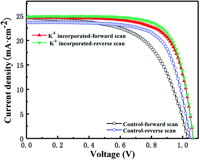 | ||
| Fig. 7 Current density–voltage (J–V) curves for representative devices of incorporated and control perovskite solar cells. | ||
| Jsc | Voc | FF | PCE | Hysteresis factor | |
|---|---|---|---|---|---|
| K+ incorporated-FS | 24.6 | 1.07 | 72.1 | 19.0 | 0.03 |
| K+ incorporated-RS | 24.8 | 1.07 | 73.6 | 19.5 | |
| Control-FS | 24.7 | 1.03 | 58.9 | 15.1 | 0.13 |
| Control-RS | 23.7 | 1.05 | 69.8 | 17.3 |
Currently, the stability is the most critical factor that limits the commercial application of perovskite solar cells. In order to investigate the stability of the perovskite solar cells, the unencapsulated devices were exposed to ambient air with a temperature of 25 °C and humidity of 40%. Except for carrying out illuminated J–V characteristics, the devices were kept in the dark.
Therefore, we can intuitively detect the dark state stability of perovskite solar cells and eliminate the effects of light and temperature. In Fig. S1 of ESI,† there are five J–V curves of control and KI incorporated devices, and we choose one of them to monitor its degradation process. From the variation of normalized PCE during the degradation process, as shown in Fig. 8, one may find that for control device, the efficiency drops rapidly to 80% within 200 h. In contrast, it takes over 1000 hours for the KI incorporated device to decay to 80% of its initial value. The absolute values of Jsc, Voc, FF and PCE for the lifetime measurements can be seen in ESI Fig. S2.† This suggests that KI incorporation is also an effective strategy to improve the long-term stability of perovskite solar cells and has an important indication in pushing forward the commercialization of organic–inorganic halide hybrid PV cells as well as modules.
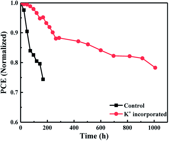 | ||
| Fig. 8 The shelf lifetime trace of the control and incorporated devices (the temperature is 25 °C and the relative humidity is 40%). | ||
Conclusions
By thoroughly investigating the properties of pristine and KI incorporated perovskite thin films/devices, the passivation mechanism of KI was illustrated. The enhanced PL peak and improved carrier lifetime of KI incorporated films suggests that the defects within the film were significantly passivated to inhibit non-radiative recombination. The KPFM results suggest that the narrowed depletion region of the grain boundary and the decreased barrier height are beneficial for the charge transportation within the films. JVT characterization proved that the internal recombination is predominant in both devices and the interface between the perovskite absorption layer and the interface of perovskite/electron transport was also significantly passivated after KI incorporation. The KI incorporation is therefore verified to be an effective solution to passivate not only the defects within the perovskite films, but also the interface of the devices. The KI passivation significantly improves the device performance (average PCE improved from 17.9% to 19.3% and hysteresis factor decreased from 0.13 to 0.03) and long-term stability (τ80 increased from less than 200 hours to over 1000 hours) of the perovskite solar cells.Conflicts of interest
There are no conflicts to declare.Acknowledgements
This work was financially supported by the Science and Technology Program of Sichuan Province (No. 2017GZ0052) and the Fundamental Research Funds for the Central Universities (No. YJ201722).References
- National Renewable Energy Laboratory, Best research-cell efficiencies, https://www.nrel.gov/pv/assets/pdfs/best-research-cell-efficiencies-190416.pdf, visited in April 2019 Search PubMed.
- A. Zhumekenov, M. Saidaminov, M. Haque, E. Alarousu, S. Sarmah, B. Murali, I. Dursun, X.-H. Miao, A. Abdelhady, T. Wu, O. Mohammed and O. Bakr, ACS Energy Lett., 2016, 1, 32–37 CrossRef CAS.
- Q. Dong, Y. Fang, Y. Shao, P. Mulligan, J. Qiu, L. Cao and J. Huang, Science, 2015, 347, 967–970 CrossRef CAS PubMed.
- S.-H. Turren-Cruz, M. Saliba, M. Mayer, H. Juárez-Santiesteban, X. Mathew, L. Nienhaus, W. Tress, M. Erodici, M.-J. Sher, M. Bawendi, M. Grätzel, A. Abate, A. Hagfeldt and J.-P. Correa-Baena, Energy Environ. Sci., 2018, 11, 78–86 RSC.
- A. Bowring, W. Tan, A. Meng, M. McGehee and P. McIntyre, ACS Appl. Mater. Interfaces, 2018, 10, 5485–5491 CrossRef PubMed.
- M. Yang, Y. Zeng, Z. Li, D. Kim, C.-S. Jiang, J. Lagemaat and K. Zhu, Phys. Chem. Chem. Phys., 2017, 19, 5043–5050 RSC.
- S. Yang, J. Dai, Z. Yu, Y. Shao, Y. Zhou, X. Xiao, X. Zeng and J. Huang, J. Am. Chem. Soc., 2019, 141, 5781–5787 CrossRef CAS PubMed.
- T. Niu, J. Lu, R. Munir, J. Li, D. Barrit, X. Zhang, H. Hu, Z. Yang, A. Amassian, K. Zhao and S. Liu, Adv. Mater., 2018, 30, e1706576 CrossRef PubMed.
- D. Lee, J. Yun, J. Kim, A. Soufiani, S. Chen, Y. Cho, X. Deng, J. Seidel, S. Lim, S. Huang and A. Ho-Baillie, ACS Energy Lett., 2018, 3, 647–654 CrossRef CAS.
- D.-Y. Son, S.-G. Kim, J.-Y. Seo, S.-H. Lee, H. Shin, D. Lee and N.-G. Park, J. Am. Chem. Soc., 2018, 140, 1358–1364 CrossRef CAS PubMed.
- Z. Tang, T. Bessho, F. Awai, T. Kinoshita, M. Maitani, R. Jono, T. Murakami, H. Wang, T. Kubo, S. Uchida and H. Segawa, Sci. Rep., 2017, 7, 12183 CrossRef PubMed.
- M. Saliba, T. Matsui, K. Domanski, J.-Y. Seo, A. Ummadisingu, S. Zakeeruddin, J.-P. Correa-Baena, W. Tress, A. Abate, A. Hagfeldt and M. Grätzel, Science, 2016, 354, 206–209 CrossRef CAS PubMed.
- T. Duong, H. Mulmudi, H. Shen, Y. Wu, C. Barugkin, Y. Mayon, H. Nguyen, D. Macdonald, J. Peng, M. Lockrey, W. Li, Y.-B. Cheng, T. White, K. Weber and K. Catchpol, Nano Energy, 2016, 30, 330–340 CrossRef CAS.
- M. Saliba, T. Matsui, J.-Y. Seo, K. Domanski, J.-P. Correa-Baena, M. Nazeeruddin, S. Zakeeruddin, W. Tress, A. Abate, A. Hagfeldt and M. Grätzel, Energy Environ. Sci., 2016, 9, 1989–1997 RSC.
- M. Deepa, M. Salado, L. Calio, S. Kazim, S. Shivaprasadc and S. Ahmad, Phys. Chem. Chem. Phys., 2017, 19, 4069–4077 RSC.
- T. Bu, X. Liu, Y. Zhou, J. Yi, X. Huang, L. Luo, J. Xiao, Z. Ku, Y. Peng, F. Huang, Y.-B. Cheng and J. Zhong, Energy Environ. Sci., 2017, 10, 2509–2515 RSC.
- G. Zheng, C. Zhu, J. Ma, X. Zhang, G. Tang, R. Li, Y. Chen, L. Li, J. Hu, J. Hong, Q. Chen, X. Gao and H. Zhou, Nat. Commun., 2018, 9, 2793 CrossRef PubMed.
- J.-J. Li, J.-Y. Ma, Q.-Q. Ge, J.-S. Hu, D. Wang and L.-J. Wan, ACS Appl. Mater. Interfaces, 2015, 7, 28518–28523 CrossRef CAS PubMed.
- T. Zhang, N. Guo, G. Li, X. Qian and Y. Zhao, Nano Energy, 2016, 26, 50–56 CrossRef CAS.
- Y. Kim, N. Jeon, J. Noh, W. Yang, J. Seo, J. Yun, A. Ho-Baillie, S. Huang, M. Green, J. Seidel, T. Ahn and S. Seok, Adv. Energy Mater., 2016, 6, 1502104 CrossRef.
- Q. Wang, B. Chen, Y. Liu, Y. Deng, Y. Bai, Q. Dong and J. Huang, Energy Environ. Sci., 2017, 10, 516–522 RSC.
- L. Zuo, H. Guo, D. deQuilettes, S. Jariwala, N. Marco, S. Dong, R. DeBlock, D. Ginger, B. Dunn, M. Wang and Y. Yang, Sci. Adv., 2017, 3, e1700106 CrossRef PubMed.
- L. Zuo, S. Dong, N. Marco, Y.-T. Hsieh, S.-H. Bae, P. Sun and Y. Yang, J. Am. Chem. Soc., 2016, 138, 15710–15716 CrossRef CAS PubMed.
- F. Zheng, W. Chen, T. Bu, K. Ghiggino, F. Huang, Y. Cheng, P. Tapping, T. Kee, B. Jia and X. Wen, Adv. Energy Mater., 2019, 1901016 CrossRef.
- C. Li, G. Chen, W. Wang, J. Zhang, L. Wu, X. Hao and L. Feng, J. Mater. Sci.: Mater. Electron., 2018, 29, 20718–20725 CrossRef CAS.
- T. Du, C. Burgess, C.-T. Lin, F. Eisner, J. Kim, S. Xu, H. Kang, J. Durrant and M. McLachlan, Adv. Funct. Mater., 2018, 28, 1803943 CrossRef.
- G. Niu, H. Yu, J. Li, D. Wang and L. Wang, Nano Energy, 2016, 27, 87–94 CrossRef CAS.
- Q. Dong, Z. Wang, K. Zhang, H. Yu, P. Huang, X. Liu, Y. Zhou, N. Chen and B. Song, Nanoscale, 2016, 8, 5552–5558 RSC.
- Q. Dong, K. Zhang, H. Yu, P. Huang, X. Liu, Y. Zhou, N. Chen and B. Song, Nanoscale, 2016, 8, 5552–5558 RSC.
- M. Abdi-Jalebi, Z. Andaji-Garmaroudi, S. Cacovich, C. Stavrakas, B. Philippe, J. Richter, M. Alsari, E. Booker, E. Hutter, A. Pearson, S. Lilliu, T. Savenije, H. Rensmo, G. Divitini, C. Ducati, R. Friend and S. Stranks, Nature, 2018, 555, 497–501 CrossRef CAS PubMed.
- D. Abou-Ras, T. Kirchartz and U. Rau, Advanced Characterization Techniques for Thin Film Solar Cells, Wiley-VCH, 2011 Search PubMed.
- C. Ding, Y. Zhang, F. Liu, Y. Kitabatake, S. Hayase, T. Toyoda, K. Yoshino, T. Minemoto, K. Katayam and Q. Shen, Nano Energy, 2018, 53, 17–26 CrossRef CAS.
- P. Dey, J. Paul, J. Bylsma, D. Karaiskaj, J. M. Luther, M. C. Beard and A. H. Romero, Solid State Commun., 2013, 165, 49–54 CrossRef CAS.
- O. Dupré, R. Vaillon and M. A. Green, Sol. Energy Mater. Sol. Cells, 2015, 140, 92–100 CrossRef.
- Z. Li, J. Tinkham, P. Schulz, M. Yang, D. Kim, J. Berry, A. Sellinger and K. Zhu, Adv. Energy Mater., 2017, 7, 1601451 CrossRef.
- Y. Shao, Z. Xiao, C. Bi, Y. Yuan and J. Huang, Nat. Commun., 2014, 5, 5784 CrossRef CAS PubMed.
- C. Li, A. Guerrero, Y. Zhong and S. Huettner, J. Phys.: Condens. Matter, 2017, 29, 193001 CrossRef PubMed.
- Y. Ju, S. Park, H. Han and H. Jung, RSC Adv., 2019, 9, 7334–7337 RSC.
- H. Li, Y. Xue, B. Zheng, J. Tian, H. Wang, C. Gao and X. Liu, RSC Adv., 2017, 7, 30422–30427 RSC.
- J.-W. Lee, S.-G. Kim, S.-H. Bae, D.-K. Lee, O. Lin, Y. Yang and N.-G. Park, Nano Lett., 2017, 17, 4270–4276 CrossRef CAS PubMed.
- J. Azpiroz, E. Mosconi, J. Bisquert and F. Angelis, Energy Environ. Sci., 2015, 8, 2118–2127 RSC.
Footnote |
| † Electronic supplementary information (ESI) available: J–V curves of five control and incorporated devices; the absolute values of Jsc, Voc, FF and PCE obtained from the degradation process of control and KI incorporated devices; JVT curves of control and KI incorporated devices during heating and cooling process. See DOI: 10.1039/c9ra05371a |
| This journal is © The Royal Society of Chemistry 2019 |