
 Open Access Article
 This Open Access Article is licensed under a Creative Commons Attribution-Non Commercial 3.0 Unported Licence
Charge transfer-induced enhancement of a Raman signal in a hybrid Ag–GaN nanostructure
Kishor Upadhyayaa,
Sharvani Sb,
Narasimha Ayachitc and
S. M. Shivaprasad *b
*b
aThin Films Lab, Centre for Materials Science, Department of Physics, B. V. Bhoomaraddi College of Engineering and Technology (Presently known as K. L. E. Technological University), Hubballi – 580031, India
bChemistry and Physics of Materials Unit, Jawaharlal Nehru Centre for Advanced Scientific Research, Bangalore-560064, India. E-mail: smsprasad@jncasr.ac.in
cCentre for Materials Science, K. L. E. Technological University, B. V. B. Campus, Hubballi – 580031, India
First published on 10th September 2019
Abstract
A hybrid system consisting of Ag nanoparticles dispersed onto a GaN nanowall network (GaN NWN) exhibited characteristic optical properties and electronic band structure. Surface-sensitive XPS studies of this high-surface-area system revealed the presence of a high surface charge carrier concentration due to dangling bonds, which resulted in a high metal-like surface conductivity. The low coverage of absorbed Ag led to the nanocluster formation, facilitating charge transfer from GaN to Ag, and thereby further increasing the surface charge carriers. Photoluminescence studies revealed the presence of a high density of band tail states at the conduction band, which is significantly (14-fold) larger than in the GaN epilayer. Raman studies show an increase (2.46-fold) in the interfacial strain at the Ag/GaN interface after the deposition of the Ag nanoparticles. We show that these surface modifications increase the density of hot spots, resulting in an intense Raman signal with an enhancement factor of 107. The role of the charge transfer between Ag nanoparticles and GaN NWN in the enhancement of Raman signal has been demonstrated.
Introduction
Metal nanoparticles have been the most sought-after materials in the past couple of decades for nano-photoelectronic applications due to the size-dependent tunability of their properties.1–3 The nanoparticles of noble metals including silver and gold exhibit properties such as surface plasmon resonance and possess a large effective scattering cross section, which make them suitable for biomolecular detection via surface enhanced Raman spectroscopy (SERS).4–7 Recent research has focused on finding a system with a suitably stable and large (area) substrate with uniformly distributed uncapped metal nanoparticles for quantitative and reliable biomolecular detection using SERS.8–11 Various materials have been used as substrates to distribute metal nanoparticles to study the enhancement of a Raman signal for different analyte molecules. A colloidal solution of Ag nanoparticles has been extensively used as a SERS substrate to detect various analytes such as valeric acid, naphthalene, phenanthrene, methimazole, ketoconazole, and 2-thiouracil. The underlying mechanism of the nanoparticle interactions with the analytes has been discussed based on experimental results using density functional theory (DFT) calculations.12–18 Several other materials, such as silicon, graphene, and actinide-embedded structures, have been used as supporting substrates for distributing Ag and Au nanoparticles to enhance the interactions between the nanoparticles and analyte molecules and consequently improve the limits of detection and enhancement factors.19–21 Similarly, the GaN thin films of various morphologies (planar and porous) have been used as supports for depositing silver nanoparticles, on which a significant enhancement in the Raman signal has been reported.22,23 This wide band-gap semiconductor is an attractive material because of its chemical resistance, high temperature/high power capability, electron saturation velocity, and internal spontaneous and piezoelectric polarization.24,25 However, studies related to the influence of the optoelectronic properties of the substrate on the characteristics of the metal nanoparticles/substrate hybrid material systems and on the enhancement of the Raman signal have been scarce.In the present study, we formed a hybrid system consisting of a GaN nanowall network (NWN) with uniformly deposited bare Ag nanoparticles. We report a comparative study of the optoelectronic properties of the GaN epilayer and GaN NWN with and without the Ag deposition of two different particle sizes. In addition to the large number of charge carriers present on the GaN NWN, we observed a charge transfer between GaN NWN and Ag, which enhanced the amount of charge carriers at the surface of the Ag/GaN hybrid system. GaN NWN substrate not only acted as a supporting substrate by providing a large surface area to form a high density of ‘hot spots’ and enabling multiple reflections within cavities22 but also contributed charge carriers to the surface of the Ag/GaN hybrid system. These large numbers of carriers at the Ag/GaN surface could exhibit plasmonic resonance upon optical excitation, leading to the observed enhancement in the Raman signal of the Rhodamine 6G (R6G) analyte.
Experimental
Nanostructured GaN thin films were grown on c-sapphire using Plasma Assisted Molecular Beam Epitaxy (SVT, USA) operating under a base pressure of 3 × 10⁻¹¹ Torr. The substrates were chemically cleaned, and then introduced into the chamber and degassed at 500 °C for 1 h. The sample was further moved to the growth chamber, where it was degassed for 30 min at 800 °C. The characteristic streaky RHEED pattern was observed, indicating the atomic cleanness of the substrate. Using growth parametric control, with a III–V ratio of 1![[thin space (1/6-em)]](https://www.rsc.org/images/entities/char_2009.gif) :100, the desired nanowall network morphology was obtained.26 The films were grown for 3 h, with Ga K-cell at 1000 °C, while the substrate was held at 630 °C with a 4.5 sccm nitrogen gas flow rate and RF plasma forward power of 375 W. The pressure of the growth chamber during the growth was 3 × 10⁻⁵ Torr. Silver nanoparticles were deposited on the network sample in an electron beam PVD system (base pressure ∼ 10−9 Torr) using an Ag wire (99.99% purity), whose coverage and size were monitored by a Quartz Crystal Microbalance. The GaN films coated by Ag were characterized for morphological images by FESEM (Quanta 3D FEG, FEI, Netherlands) at 20 kV. The morphology and particle size distribution of the samples were analyzed using the Imagej software. X-ray photoelectron spectroscopy (EAC 2000 SPHERA 547 spectrometer) with an X-ray spot diameter of 3–4 mm was used to study the electronic structure using an Al K-alpha anode. The binding energies were calibrated by measuring the Fermi energy on a silver foil in electrical contact with the sample. The analyzer was kept normal to the surface of the samples, and the spectra were recorded with a constant analyzer pass-energy of 100 eV for survey scans and 25 eV for valence band scans. Optical properties were studied using a photoluminescence spectrometer (Horiba Scientific, Japan) with a He–Cd laser using 325 nm excitation at 8 mW power. Raman spectra (inVia, Renishaw, UK) were recorded in the 180° backscattering geometry using a 532 nm excitation from a Nd:YAG solid state laser (∼8 mW power) with a grating monochromator (2400/1800 grooves per mm) and Peltier-cooled CCD detector, and the acquisition time was 30 s. 1 μl of different concentrations of Rhodamine 6G was drop-cast on the samples and dried for 1 h before the Raman spectrum was acquired for SERS studies.
:100, the desired nanowall network morphology was obtained.26 The films were grown for 3 h, with Ga K-cell at 1000 °C, while the substrate was held at 630 °C with a 4.5 sccm nitrogen gas flow rate and RF plasma forward power of 375 W. The pressure of the growth chamber during the growth was 3 × 10⁻⁵ Torr. Silver nanoparticles were deposited on the network sample in an electron beam PVD system (base pressure ∼ 10−9 Torr) using an Ag wire (99.99% purity), whose coverage and size were monitored by a Quartz Crystal Microbalance. The GaN films coated by Ag were characterized for morphological images by FESEM (Quanta 3D FEG, FEI, Netherlands) at 20 kV. The morphology and particle size distribution of the samples were analyzed using the Imagej software. X-ray photoelectron spectroscopy (EAC 2000 SPHERA 547 spectrometer) with an X-ray spot diameter of 3–4 mm was used to study the electronic structure using an Al K-alpha anode. The binding energies were calibrated by measuring the Fermi energy on a silver foil in electrical contact with the sample. The analyzer was kept normal to the surface of the samples, and the spectra were recorded with a constant analyzer pass-energy of 100 eV for survey scans and 25 eV for valence band scans. Optical properties were studied using a photoluminescence spectrometer (Horiba Scientific, Japan) with a He–Cd laser using 325 nm excitation at 8 mW power. Raman spectra (inVia, Renishaw, UK) were recorded in the 180° backscattering geometry using a 532 nm excitation from a Nd:YAG solid state laser (∼8 mW power) with a grating monochromator (2400/1800 grooves per mm) and Peltier-cooled CCD detector, and the acquisition time was 30 s. 1 μl of different concentrations of Rhodamine 6G was drop-cast on the samples and dried for 1 h before the Raman spectrum was acquired for SERS studies.
Results and discussion
Ag nanoparticles of two different sizes were deposited onto the GaN nanowall network. Fig. 1 shows FESEM images of the network morphologies of the bare GaN nanowall network and two different coverage levels of Ag on GaN. The interfacial tensile stress between GaN and sapphire, which are 16% lattice mismatched, results in a dense network of GaN nanowalls due to the formation of open screw dislocations as a strain relaxation pathway.27 These wedge-shaped nanowalls are 5–10 nm wide at the tips and 100–150 nm wide at the base with a height of ∼1 μm. The calculated surface area of these walls is 80- to 100-fold greater than that of the GaN epilayer. Upon Ag deposition, the measured average size of the Ag nanoparticles is 13 nm and 25 nm for the first (Fig. 1b) and second (Fig. 1c) coverage levels, respectively. The average interparticle spacing between these nanoparticles is 5 nm and 10 nm for the first and second coverages, respectively, which indicates that the Ag nanoparticles are uniformly distributed and densely populated on the nanowalls. The electron concentration was estimated by Hall measurements on bare GaN in the nanowall network configuration to be ∼1019 cm−3. This high carrier concentration is attributed to the large density of surface dangling bonds caused by nitrogen vacancies.28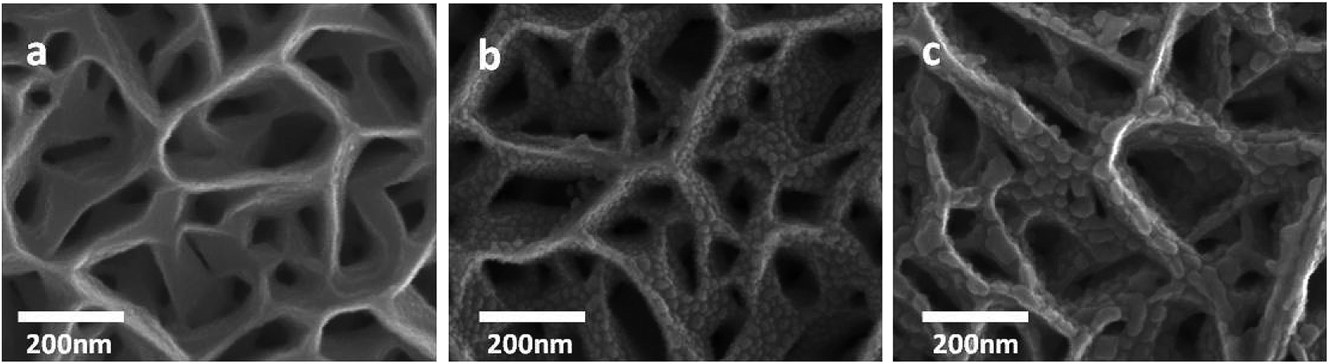 | ||
| Fig. 1 FESEM images of (a) GaN nanowall network (b) GaN network with 13 nm Ag nanoparticles and (c) GaN network with 25 nm Ag nanoparticles. | ||
Fig. 2 shows XPS valence band spectra for the GaN flat epilayer, GaN NWN, Ag 13 nm/GaN and Ag 25 nm/GaN. The spectrum for the epilayer has a peak at 4.06 eV, which corresponds to the N 2p–Ga 4p hybridized state, and two N 2p–Ga 4s hybridized peaks at 8.16 eV and 9.58 eV.29,30 The binding energy values of these peaks shift to 4.7 eV, 8.7 eV and 10.1 eV, respectively, in the case of GaN NWN, which has a more electronically stable structure. After deposition of 13 nm and 25 nm Ag nanoparticles, the occupied states in the valence band maxima shift by 0.3 eV towards the lower binding energy scale with respect to that of the epilayer, which signifies a comparative shift in the Fermi level of both the Ag/GaN samples towards conduction band minima. A strong peak is observed at 4.8 eV, which corresponds to the Ag 4d shallow core-level, and a lower intensity peak is observed for the 25 nm Ag nanoparticles. The Ga 3d core-level peak is observed at 19.7 eV and 20.1 eV for the epilayer and GaN nanowall, respectively. These peak values shift to 20.6 eV and 20.5 eV for Ag 13 nm/GaN and Ag 25 nm/GaN, respectively. This higher binding energy shift of the Ga 3d core level signifies a decrease in the upward surface band bending, as shown in the schematic band diagram (Fig. 6),31–33 and results in a lowering of the barrier height and contact resistance.31,32 An additional peak observed at −5.70 eV upon deposition of the Ag nanoparticles corresponds to the degenerately occupied electron states in the conduction band of the Ag/GaN system. This additional peak along with the higher binding energy shift in the Ga core level spectra as discussed above indicate a charge transfer from GaN to Ag at the surface, thereby increasing the cumulative number of surface electrons in the Ag/GaN hybrid system that contribute to plasmonic resonance upon optical illumination.
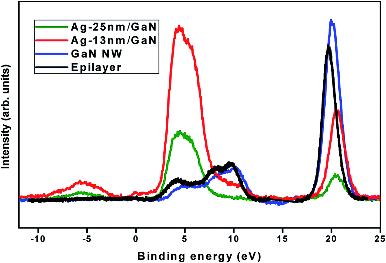 | ||
| Fig. 2 Valence band and Ga 3d core level spectra of GaN epilayer, GaN nanowall network, Ag 13 nm/GaN and Ag 25 nm/GaN samples acquired by X-ray photoelectron spectroscopy. | ||
Fig. 3 shows a comparison of the PL spectra between the band-edge emission of GaN NWN and the GaN epilayer sample with 2 μm thickness. The PL emission of the flat GaN epilayer film, which has a large dislocation density (∼109 cm−2), is less intense and has a very narrow FWHM in comparison to that of the GaN NWN. The high intensity emission (∼14 times larger) from the nanowalls is attributed to the low level of defects and low strain of the nanowalls, while the broad FWHM compared to that of the epilayer arises due to a high density of band tail states in the conduction band.34 Upon the deposition of the Ag nanoparticles, the band-edge emission for the Ag-13 nm/GaN sample decreases by 35% and further decreases by 75% for the Ag-25 nm/GaN sample compared to the GaN NWN sample. No change in the FWHM in either of the Ag-deposited samples is observed compared to that of GaN NWN. This reduction in the intensity upon the deposition of the Ag nanoparticles is attributed to a combination of charge transfer-induced conduction band filling, as evident from the XPS and Ag nanoparticles acting as traps, to the band edge emission from GaN NWN underneath them.35,36 This characteristic enables the recombination of electron–hole pairs, thereby reducing their numbers and resulting in an observed intensity loss of the PL signal. The previously mentioned unchanged large FWHM for all three samples as compared to those of the epilayer is attributed to the broad conduction band of electrons that recombine with holes in the valence band.
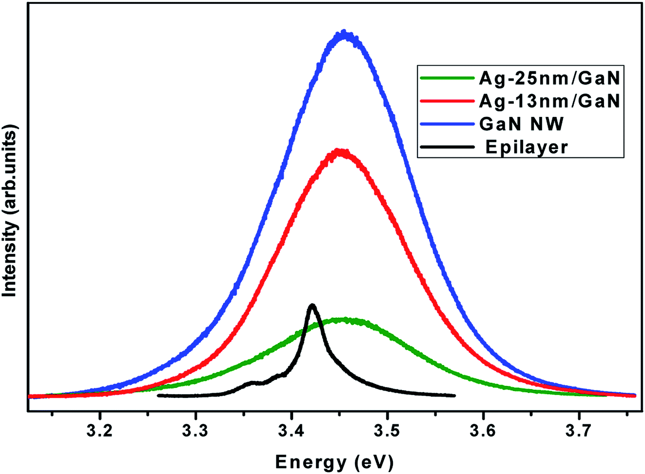 | ||
| Fig. 3 Photoluminescence band-edge emission spectra of GaN epilayer, GaN nanowall network, Ag-13 nm/GaN and Ag-25 nm/GaN samples. | ||
Fig. 4 shows E2 (high) Raman spectra for GaN NWN, Ag-13 nm/GaN and Ag-25 nm/GaN. The E2 (high) peak appearing around 570 cm−1 is due to the vibration of the N atoms of GaN. Using the shift of this peak with respect to that of powdered GaN, we calculate the stress values (σa) of our samples using the Kozawa relation,37
| ΔE2 = σa × (4.2 ± 0.3) cm−1 GPa−1 |
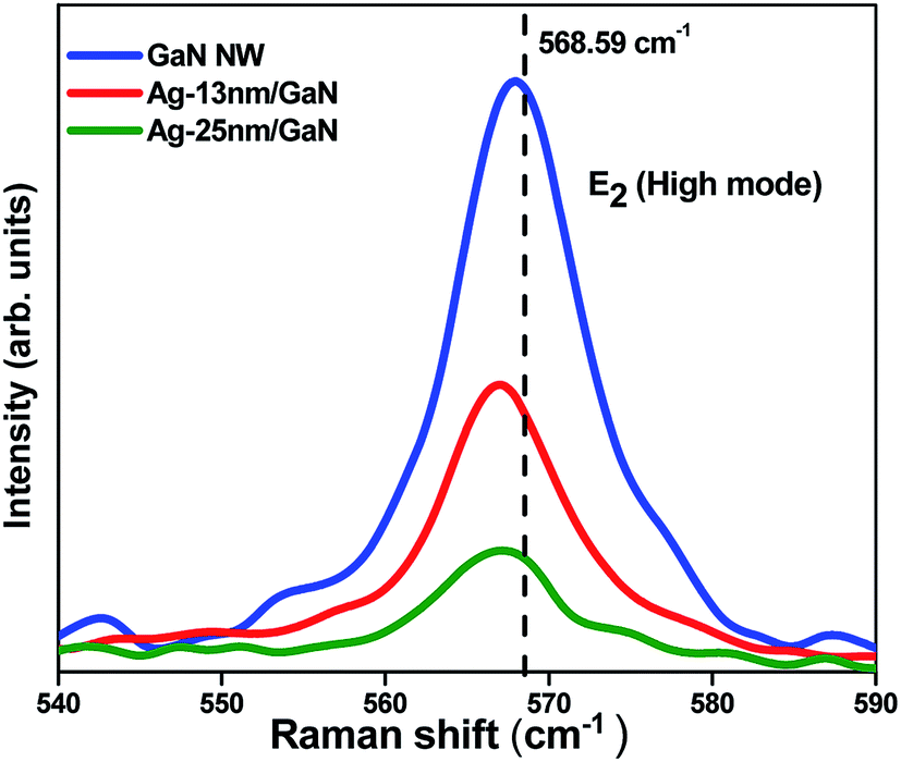 | ||
| Fig. 4 Raman spectra showing E2 (high) mode of GaN nanowall network, Ag-13 nm/GaN and Ag-25 nm/GaN samples. | ||
The peak for E2 (high) mode for the epilayer appears at 568.59 cm−1. Table 1 shows the shift in the wavenumber as well as the estimated stress values.
| Sample | E2 (high) cm−1 | Raman shift (ΔE2) in cm−1 | Stress (σa) in GPa |
|---|---|---|---|
| GaN NWN | 567.9 | 0.63 | 0.15 |
| Ag-13 nm/GaN | 567 | 1.59 | 0.37 |
| Ag-25 nm/GaN | 567 | 1.59 | 0.37 |
It is evident from the Table 1 that GaN NWN exhibits a Raman shift of 0.63 cm−1 compared to GaN epilayer due to the tensile strain, as mentioned earlier. Because of the absence of nitrogen atoms or excess gallium (Ga to N ratio = 1.75, calculated from XPS results), phonon localization may also be responsible for this observed shift. After the deposition of Ag, the shift increases to 1.59 cm−1 for both the Ag-deposited samples. This shift of 0.96 cm−1 with respect to that of the bare GaN NWN is due to the increased interfacial strain caused by the deposition of the Ag nanoparticles.
In order to observe the enhancement in the Raman signal of Ag/GaN substrate, Rhodamine 6G dye (10−4 M) was dropped on the bare GaN NWN and Ag-13 nm/GaN samples. The increase in the Raman signal is quantified by the enhancement factor (EF), which is based on the relative intensity of the Raman spectra with respect to that of analyte molecule for a specific peak and ratio of number of molecules probed in bulk with SERS experiments.22 The calculated enhancement factor for the Ag-13 nm/GaN sample for the R6G analyte is 1 × 10⁷. This enhancement of the Raman signal is a combined effect of the dense and uniform distribution of the Ag nanoparticles on the GaN nanowalls along with the large surface area and additional surface electron concentration that occurs due to the charge transfer between the Ag nanoparticles and GaN nanowalls network. This increases the density of hot spots, which in turn increases the number of adsorbed molecules on the sample and hence enhances the Raman signal. Raman spectra are shown in Fig. 5 corresponding to the bare GaN and Ag-13 nm/GaN samples. The bare GaN nanowall network showed minimal Raman features with the R6G molecule whereas Ag-13 nm/GaN showed distinct and intense vibrational peaks. The peak observed at 1195 cm−1 corresponds to C–H in-plane bending, while the peaks from 1318 to 1666 cm−1 are due to the C–C stretching of the aromatic ring of the R6G molecule.38 The peaks at 622 cm−1 and 782 cm−1 appear due to the in-plane and out-of-plane bending motions of carbon and hydrogen atoms of the xanthene skeleton, respectively.39 As we see in Fig. 5, the Raman spectra acquired from the Ag/GaN sample shows a huge enhancement in the signal compared to that of the bare GaN substrate, which is due to the surface plasmon resonance exhibited by the Ag nanoparticles and the large number of free electrons present on the GaN NWN surface. The high surface area of the GaN nanowalls substrate, uniform distribution of high-density Ag nanoparticles and the additional free electrons that accumulate on the surface of Ag/GaN film contribute to the enhancement in the Raman signal.
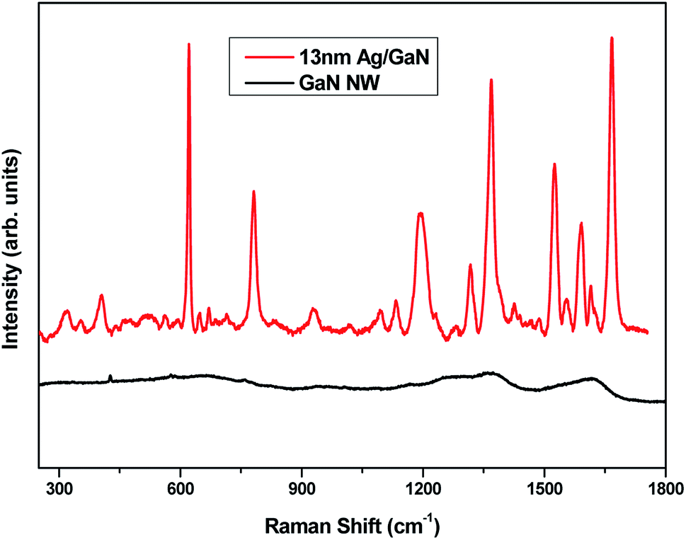 | ||
| Fig. 5 Comparison of Raman spectra acquired for GaN nanowall network and Ag-13 nm/GaN sample with R6G dye (10−4 M). | ||
Fig. 6 shows the schematic band structure of the epilayer, GaN NWN, Ag-13 nm/GaN and Ag-25 nm/GaN samples, which are derived from the valence band spectra of the XPS results (Fig. 2) and photoluminescence spectra (Fig. 3). It is evident from the figure that all of the samples are n-type since the Fermi level lies close to their respective conduction bands. The Fermi level of the GaN network sample coincides with the conduction band minima; this occurs because of the large charge (electron) carrier concentration on the surface that results from the nitrogen vacancies, as evidenced by the Ga-to-N ratio (1.75) calculated from XPS. In the case of the epilayer, the Fermi level lies 0.52 eV lower than the conduction band minimum, indicating a lesser n-type behaviour compared to GaN NWN. The Ga 4p–N 2p hybridized bands of GaN NWN appear at higher binding energies (shift of 0.6 eV) compared to that of the epilayer, suggesting a more electronically relaxed structure. This result is due to the charge transfer between Ga 4p and N 2p, which leads to a shift in the valance band maxima away from the Fermi level and consequently the coincidence of the conduction band minimum with the Fermi level of the GaN NWN. After depositing 13 nm Ag on GaN, the Fermi level shifts away from the conduction band minimum as compared to that of GaN NWN and shifts further away with the 25 nm Ag deposition. A clear broadening of the conduction band for both of the Ag-deposited GaN substrates is observed due to the charge transfer from GaN and Ag to the conduction band, resulting in a photoemission peak at −5.6 eV. These transferred charges act as free electrons at the surface of the Ag/GaN system, which causes surface plasmon resonance and leads to the Raman signal enhancement observed in the Raman studies.
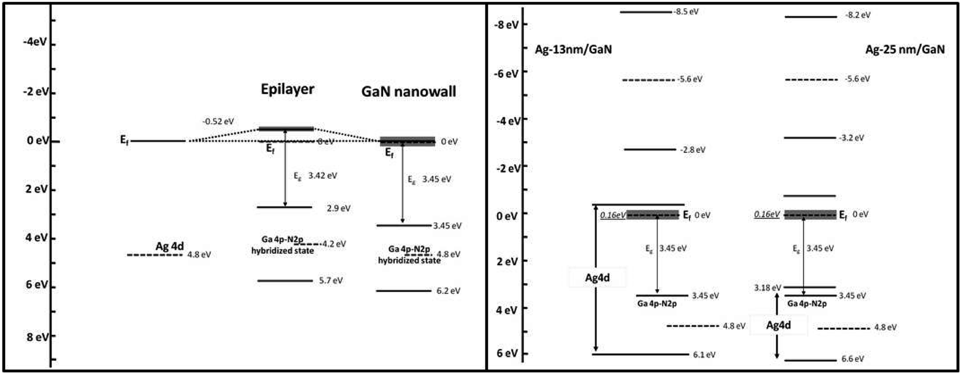 | ||
| Fig. 6 Schematic band structure of the epilayer, GaN nanowall network, Ag-13 nm/GaN and Ag-25 nm/GaN samples. | ||
Conclusions
In summary, a comparative study of different GaN substrates (planar and nanowall network) with different morphologies and distributions of Ag nanoparticles (13 and 25 nm) was performed in order to study the role of surface properties of GaN nanowall network in the enhancement of the Raman signal. XPS results show that GaN NWN possessing a high carrier concentration (∼1019 cm−3) facilitated the charge transfer from GaN to the Ag conduction band due to surface band bending at the Ag/GaN interface upon Ag nanoparticles deposition, which led to the accumulation of a high-density free electrons on the surface of the Ag/GaN hybrid system. Photoluminescence spectra of GaN NWN reveal the presence of a high density of band tail states at the conduction band, which is significantly (14-fold) larger than that of the GaN epilayer. Raman studies show a 2.46-fold increase in the interfacial strain upon the deposition of Ag nanoparticles on GaN NWN. The enhancement factor of the Raman signal is calculated to be 107 for Rhodamine 6G analyte molecules. A high density of free electrons on the Ag/GaN surface aided by the charge transfer, the large surface area of the GaN NWN substrate, and the uniform distribution of highly dense Ag nanoparticles promote surface plasmon resonance, which led to the observed enhancement. This study shows the potential of employing the Ag/GaN-NWN hybrid system for bioanalytical and biochemical sensing applications. Further work to tune the band edge emission in GaN by alloying with indium to enhance its coupling with the surface plasmons is in progress.Conflicts of interest
There are no conflicts to declare.Acknowledgements
The authors thank Prof. C. N. R. Rao for the support and encouragement for this study. The authors thank Dr Sandeep Dhara, Indira Gandhi Centre for Atomic Research, Kalpakkam for their kind support regarding Raman studies. One of the authors (Kishor Upadhyaya) thanks VGST and TEQIP for its financial support.References
- J. A. Scholl, A. L. Koh and J. A. Dionne, Quantum plasmon resonances of individual metallic nanoparticles, Nature, 2012, 483, 421–427 CrossRef CAS PubMed.
- F. Javier García de Abajo, Plasmons go quantum, Nature, 2012, 483, 417–418 CrossRef PubMed.
- J. Bosbach, C. Hendrich, F. Stietz, T. Vartanyan and F. Träger, Ultrafast Dephasing of Surface Plasmon Excitation in Silver Nanoparticles: Influence of Particle Size, Shape, and Chemical Surrounding, Phys. Rev. Lett., 2002, 89, 257404 CrossRef CAS PubMed.
- K. Hering, et al., SERS: a versatile tool in chemical and biochemical diagnostics, Anal. Bioanal. Chem., 2008, 390, 113–124 CrossRef CAS PubMed.
- A. Kawabata and R. Kubo, Electronic Properties of Fine Metallic Particles. II. Plasma Resonance Absorption, J. Phys. Soc. Jpn., 1966, 21, 1765–1772 CrossRef CAS.
- P. K. Jain and M. A. El-Sayed, Plasmonic coupling in noble metal nanostructures, Chem. Phys. Lett., 2010, 487, 153–164 CrossRef CAS.
- L. Vigderman and E. R. Zubarev, Starfruit-Shaped Gold Nanorods and Nanowires: Synthesis and SERS Characterization, Langmuir, 2012, 28, 9034–9040 CrossRef CAS PubMed.
- C. Noguez, Surface Plasmons on Metal Nanoparticles: The Influence of Shape and Physical Environment, J. Phys. Chem. C, 2007, 111, 3806–3819 CrossRef CAS.
- K. Lance Kelly, E. Coronado, L. L. Zhao and G. C. Schatz, The Optical Properties of Metal Nanoparticles: The Influence of Size, Shape, and Dielectric Environment, J. Phys. Chem. B, 2003, 107, 668–677 CrossRef.
- J. A. Huang, Y. Q. Zhao, X. J. Zhang, L. F. He, T. L. Wong, Y. S. Chui, W. J. Zhang and S. T. Lee, Ordered Ag/Si Nanowires Array: Wide-Range Surface-Enhanced Raman Spectroscopy for Reproducible Biomolecule Detection, Nano Lett., 2013, 13, 5039–5045 CrossRef CAS PubMed.
- C. S. Rout, A. Kumar and T. S. Fisher, Carbon nanowalls amplify the surface-enhanced Raman scattering from Ag nanoparticles, Nanotechnology, 2011, 22, 395704 CrossRef PubMed.
- M. Kamran, et al., Characterization of valeric acid using substrate of silver nanoparticles with SERS, J. Mol. Liq., 2019, 273, 536–542 CrossRef CAS.
- A. T. Onawole, S. A. Popoola, T. A. Saleh and A. A. Al-Saadi, Silver-loaded graphene as an effective SERS substrate for clotrimazole detection: DFT and spectroscopic studies, Spectrochim. Acta, Part A, 2018, 201, 354–361 CrossRef CAS PubMed.
- K. Haruna, T. A. Saleh, M. K. Hossain and A. A. Al-Saadi, Hydroxylamine reduced silver colloid for naphthalene and phenanthrene detection using surface-enhanced Raman spectroscopy, Chem. Eng. J., 2016, 304, 141–148 CrossRef CAS.
- K. Haruna, T. A. Saleh, J. A. Thagfi and A. A. Al-Saadi, Structural properties, vibrational spectra and surface-enhanced Raman scattering of 2,4,6-trichloro- and tribromoanilines: a comparative study, J. Mol. Struct., 2016, 1121, 7–15 CrossRef CAS.
- T. A. Saleh, M. M. Al-Shalalfeh and A. A. Al-Saadi, Silver nanoparticles for detection of methimazole by surface-enhanced Raman spectroscopy, Mater. Res. Bull., 2017, 91, 173–178 CrossRef CAS.
- M. M. Al-Shalalfeh, A. T. Onawole, T. A. Saleh and A. A. Al-Saadi, Spherical silver nanoparticles as substrates in surface-enhanced Raman spectroscopy for enhanced characterization of ketoconazole, Mater. Sci. Eng. C, 2017, 76, 356–364 CrossRef CAS PubMed.
- M. M. Al-Shalalfeh, T. A. Saleh and A. A. Al-Saadi, Silver colloid and film substrates in surface-enhanced Raman scattering for 2-thiouracil detection, RSC Adv., 2016, 6, 75282–75292 RSC.
- Y. Bu, et al., Silver-Nanoparticle-Embedded Porous Silicon Disks Enabled SERS Signal Amplification for Selective Glutathione Detection, ACS Appl. Nano Mater., 2018, 1(1), 410–417 CrossRef CAS.
- X. Yue, et al., Synthesis of a low-cost, stable, silicon-based SERS substrate for rapid, nondestructive biosensing, Optik, 2019, 192, 162959 CrossRef CAS.
- Y. Gao, L. Chen, X. Dai, R. Song, B. Wang and Z. Wang, A strong charge-transfer effect in surface-enhanced Raman scattering induced by valence electrons of actinide elements, RSC Adv., 2015, 5, 32198–32204 RSC.
- S. Siddhanta, V. Thakur, C. Narayana and S. M. Shivaprasad, Universal Metal-Semiconductor Hybrid Nanostructured SERS Substrate for Biosensing, ACS Appl. Mater. Interfaces, 2012, 4, 5807–5812 CrossRef CAS PubMed.
- S. Sharvani, K. Upadhayaya, G. Kumari, C. Narayana and S. M. Shivaprasad, Nano-morphology induced additional surface plasmon resonance enhancement of SERS sensitivity in Ag/GaN nanowall network, Nanotechnology, 2015, 26, 465701 CrossRef CAS PubMed.
- B. S. Kang, H. T. Wang, F. Ren and S. J. Pearton, Electrical detection of biomaterials using AlGaN/GaN high electron mobility transistors, J. Appl. Phys., 2008, 104, 031101 CrossRef.
- M. E. Sharifabad, et al., Sains Malays., 2011, 40(3), 267 CAS.
- M. Kesaria, S. Shetty and S. M. Shivaprasad, Evidence for Dislocation Induced Spontaneous Formation of GaN Nanowalls and Nanocolumns on Bare C-Plane Sapphire, Cryst. Growth Des., 2011, 11, 4900–4903 CrossRef CAS.
- M. Kesaria and S. M. Shivaprasad, Nitrogen flux induced GaN nanostructure nucleation at misfit dislocations on Al2O3(0001), Appl. Phys. Lett., 2011, 99, 143105 CrossRef.
- H. P. Bhasker, S. Dhar, A. Sain, M. Kesaria and S. M. Shivaprasad, High electron mobility through the edge states in random networks of c-axis oriented wedge-shaped GaN nanowalls grown by molecular beam epitaxy, Appl. Phys. Lett., 2012, 101, 132109 CrossRef.
- V. Thakur and S. M. Shivaprasad, Electronic structure of GaN nanowall network analysed by XPS, Appl. Surf. Sci., 2015, 327, 389–393 CrossRef CAS.
- V. Venugopal, K. Upadhyaya, K. Kumar and S. M. Shivaprasad, Ion induced compositional changes and nanodroplet formation on GaN surface, Appl. Surf. Sci., 2014, 315, 440–444 CrossRef CAS.
- Z. Zhang and J. T. Yates Jr, Band Bending in Semiconductors: Chemical and Physical Consequences at Surfaces and Interfaces, Chem. Rev., 2012, 112, 5520–5551 CrossRef CAS PubMed.
- G. Margaritondo, F. Gozzo and C. Coluzza, Band bending at semiconductor interfaces and its effect on photoemission line shapes, Phys. Rev. B: Condens. Matter Mater. Phys., 1993, 47, 9907–9909 CrossRef PubMed.
- R. Huang, et al., Angular Dependent XPS study of surface band bending on Ga-polar and n-GaN, Appl. Surf. Sci., 2018, 440, 637–642 CrossRef CAS.
- V. Thakur, M. Kesaria and S. M. Shivaprasad, Enhanced band edge luminescence from stress and defect free GaN nanowall network morphology, Solid State Commun., 2013, 171, 8–13 CrossRef CAS.
- A. Ganguly, A. Mondal, J. C. Dhar, N. K. Singh and S. Choudhury, Enhanced visible light absorption by TiO2 film patterned with Ag nanoparticles arrays, Physica E, 2013, 54, 326–330 CrossRef CAS.
- W. Zhou, H. Liu, J. Wang, D. Liu, G. Du and J. Cui, Ag2O/TiO2 Nanobelts Heterostructure with Enhanced Ultraviolet and Visible Photocatalytic Activity, ACS Appl. Mater. Interfaces, 2010, 2, 2385–2392 CrossRef CAS PubMed.
- C. Kisielowski, J. Krüger, S. Ruvimov, T. Suski, J. W. Ager III, E. Jones, Z. Liliental Weber, M. Rubin, E. R. Weber, M. D. Bremser and R. F. Davis, Strain-related phenomena in GaN thin films, Phys. Rev. B: Condens. Matter Mater. Phys., 1996, 54, 17745 CrossRef CAS PubMed.
- E. Kirubha and P. K. Palanisam, Silver nanoparticles: synthesis, properties, toxicology, applications and perspectives, Adv. Nat. Sci.: Nanosci. Nanotechnol., 2014, 5, 4 Search PubMed.
- S. Cong, et al., Noble metal-comparable SERS enhancement from semiconducting metal oxides by making oxygen vacancies, Nat. Commun., 2015, 6, 7800 CrossRef CAS PubMed.
| This journal is © The Royal Society of Chemistry 2019 |