
 Open Access Article
 This Open Access Article is licensed under a Creative Commons Attribution-Non Commercial 3.0 Unported Licence
Improved photoelectric performance of all-inorganic perovskite through different additives for green light-emitting diodes†
Xianqi Yang,
Huaimin Gu *,
Shuti Li,
Jihang Li,
Hengzhi Shi,
Jinyuan Zhang,
Nana Liu,
Zebing Liao,
Wenzhu Xu and
Yuan Tan
*,
Shuti Li,
Jihang Li,
Hengzhi Shi,
Jinyuan Zhang,
Nana Liu,
Zebing Liao,
Wenzhu Xu and
Yuan Tan
Institute of Semiconductor Science and Technology, South China Normal University, Guangzhou, Guangdong, China. E-mail: guhm139@139.com
First published on 25th October 2019
Abstract
The exceptional optical and electronic properties of all-inorganic cesium lead bromide (CsPbBr3) perovskite make it an ideal new optoelectronic material, but low surface coverage limits its performance. The morphological characteristics of thin films have a great influence on the performance of perovskite light emitting diodes, especially at low coverage, and an inhomogeneous surface will lead to current leakage. To tackle this problem, the widespread adoption of composite layers including polymers poly(ethylene oxide) (PEO) and organic insulating poly(vinylpyrrolidone) (PVP) and all-inorganic perovskites is an effective way to increase the surface coverage and uniformity of perovskite films and improve the performance of perovskite light emitting devices. In our work, the perovskite thin films are investigated by using PEO and PVP dual additives, and the optimized CsPbBr3–PEO–PVP LED with maximum luminance, current efficiency, and external quantum efficiency of 2353 cd m−2 (at 7.2 V), 2.14 cd A−1 (at 6.5 V) and 0.85% (at 6.5 V) was obtained. This work indicates that the method of using additives is not only the key to enhancing the quality of perovskite thin film, but also the key to achieving a higher performance perovskite LED.
Introduction
In recent years, organic–inorganic hybrid perovskites have attracted significant scientific attention in the field of solar cells and light emitting diodes. The perovskite materials show that they have tremendous prospects in optoelectronic devices because of their superior optoelectronic properties.1–5 However, organic–inorganic hybrid perovskite materials are more easily degraded in air, which leads to a decrease of device stability. In contrast, all-inorganic cesium–lead halide perovskite (CsPbX3, X = Cl, Br, I) has been proven to have better stability and excellent photoelectric properties, such as high colour purity with narrow spectral width (full width at half maximum, FWHM, of ≈20 nm), high absorption coefficients, long diffusion length and tunability of the band gap.5–9 Hence, the investigation of all-inorganic cesium–lead halide perovskite may lay the foundation for the development of high-performance and stable perovskite light-emitting diodes.10Although all-inorganic perovskite has unique advantages in heat resistance and environmental adaptability which enhance the stability of devices, the preparation process is difficult to master accurately. It may lead to poor perovskite films in spin-coating precursor process, resulting in high leakage currents and low efficiencies in device.7,11 Various approaches have been reported, such as using a mixed-cation perovskite on top of a hydrophilic polymer for better wetting and surface coverage.12 There is still a lack of control over the perovskite precipitation and crystallization, because the precursors are pre-mixed and deposited as a whole, thereby leading to formation of non-uniform and inhomogeneous film morphologies. Besides, various synthetic methods of Cs–perovskite have been developed, such as anion exchange, room-temperature precipitation, solvothermal, etc.13 Wu et al. have reported a water triggered CsX (X = Cl, Br, or I) stripping approach to convert the non-luminescent Cs4PbX6 into monodisperse luminescent CsPbBr3 NCs.14 Li et al. have utilized a room-temperature supersaturated recrystallization method (free of inert gas and injection operation) to control the size of all-inorganic perovskite QDs and have successfully fabricated efficient perovskite LEDs.15 Dr Y. Shi designed a new concept, IPI, that is, a pair of ultrathin insulator layers (LiF) sandwiching the perovskite film. As a result, a 30-fold enhancement in current efficiency of IPI structured PeLEDs over conventional one was achieved from 0.64–20.3 cd A−1.36
Despite remarkable development of all-inorganic perovskite LED, there are still many factors that limit its application. At the electronic field, the stability of perovskite LED is largely determined by thin film surface coverage. Relevant researches show that pinholes in perovskite emissive layer can engender short circuits of devices, which is the main reason for hindering the development of all-inorganic perovskite LED. In order to improve the quality of the thin film, researchers have developed a pinhole-free uniform perovskite film by continuous deposition, which can greatly improve device efficiency.16,17 However, the pinholes and incompleteness of thin films have not been completely solved, especially for solution-based processing technology. Therefore, in order to promote the application of the all-inorganic perovskite film, the most urgent problem to be solved at present is to develop a smooth, complete, uniform and pinhole-free perovskite thin film. So far, it is still a challenging task for the development of all-inorganic perovskite LED. It is noteworthy that researchers have been reporting various new methods of solving this problem by mixing polymers with perovskite, including poly(9-vinylcarbazole) (PVK),18–20 a dielectric polymer matrix of polyimide precursor dielectric (PIP),21 poly methyl methacrylate (PMMA),22,23 polyethylene oxide (PEO),24–26,34 polyethyleneimine (PEI),27,28 etc. Nonetheless, there are still plenty of shortcomings of discontinuous coverage and current leakage in the perovskite emissive layer, which prevent perovskite LEDs from reaching a high luminance intensity.9
In this paper, the smooth, homogeneous, pinhole-free perovskite composite emissive layer consisting of cesium lead tribromide (CsPbBr3), poly(ethylene oxide) (PEO), and poly(vinylpyrrolidone) (PVP) was investigated. The LEDs were developed with an indium tin oxide (ITO) anode, CsPbBr3–PEO–PVP composite emissive layer, PEDOT:PSS hole transporting layer (HTL), TPBi electron transporting layer (ETL) and LiF/Ag cathode. Furthermore, CsPbBr3–PEO–PVP thin films were developed using the different proportion of additives, and the relationships between device performance and the crystallinity of CsPbBr3–PEO–PVP thin films were studied. The optimized CsPbBr3–PEO–PVP LED achieved maximum luminance, current efficiency, and external quantum efficiency of 2353 cd m−2 (at 7 V), 2.14 cd A−1 (at 6.5 V) and 0.85 (at 6.5 V). Compared with CsPbBr3–PEO–TPBI perovskite LED devices,13 our work is to apply CsPbBr3–PEO–PVP thin films in the structure of ITO/PEDOT:PSS/Perovskite/TPBI/LiF/Al and achieve higher performance, including current efficiency, EQE and stability. On the other hand, compare with relevant research,20 the coverage of our perovskite films has been significantly improved. Theoretically, the electrical properties of the devices can be expected to be further improved. It is one of the urgent work that we need to carry out in the future.
Experimental
Materials
Cesium bromide (CsBr, 99%) and lead bromide (PbBr2, 99.99%) were purchased from Xi'an Polymer Light Technology Corp. Polyethylene oxide (PEO, Mw = 400![[thin space (1/6-em)]](https://www.rsc.org/images/entities/char_2009.gif) 000), Polymer Polyvinyl Pyrrolidone (PVP, Mw = 1300000), 1,3,5-tris(2-N-phenylbenzimidazolyl)-benzene (TPBi), poly(2,3-dihydrothieno-1,4-dioxin)-poly(styrenesulfonate) (PEDOT:PSS, AI4803) and dimethyl sulfoxide (DMSO, ≥99.9%) were purchased from Sigma-Aldrich. All the materials were directly used without any further purifications.
000), Polymer Polyvinyl Pyrrolidone (PVP, Mw = 1300000), 1,3,5-tris(2-N-phenylbenzimidazolyl)-benzene (TPBi), poly(2,3-dihydrothieno-1,4-dioxin)-poly(styrenesulfonate) (PEDOT:PSS, AI4803) and dimethyl sulfoxide (DMSO, ≥99.9%) were purchased from Sigma-Aldrich. All the materials were directly used without any further purifications.
Precursor preparation
CsBr and PbBr2 with a molar ratio of 2:1 (0.7 M) were first mixed in DMSO and then mixed with PEO in four different weight ratio (1:0.009 to 1:0.024) to prepare the CsPbBr3–PEO precursor solution. The CsPbBr3–PEO solution with optimized ratio was further blended with PVP in varied weight ratios (1:0.03 to 1:0.12) to furnish the CsPbBr3–PEO–PVP precursor solution.
Film preparation and device fabrication
ITO-patterned glass substrates were cleaned sequentially with detergent water, acetone, and ethanol for 30 min by sonication, then dried with nitrogen and followed by oxygen plasma treatment for 20 min before using. All the devices were fabricated with multilayers structure consisting of ITO/PEDOT:PSS/Perovskite/TPBi/LiF/Ag. The PEDOT:PSS (40 nm) was spin-coated onto ITO substrates at 3000 rpm for 50 s, following by annealing at 140 °C for 20 min in air to remove the residual water. After cooling down, all the perovskite films based on CsPbBr3 were fabricated on PEDOT:PSS film in an N2-filled glove box. For CsPbBr3 films, CsPbBr3–PVP films, CsPbBr3–PEO films and CsPbBr3–PEO–PVP films, optical transparent precursor solutions were spin-coated onto the substrate at 3000 rpm for 60 s, and annealed at 80 °C for 10 min to remove the residual solvent. Finally, the device fabrication process was finished by depositing TPBi (40 nm), LiF (1 nm), and Ag (100 nm) layers in thermal evaporation chamber with vacuum pressure below 2 × 10⁻⁶ mbar. The active area of the device is 0.08 cm2.Film characterization and device measurements
XRD spectra were obtained by X-ray diffractometer with a Cu Kα source (PANalytical B.V. Empyrean). The morphology of perovskite films was studied using a Zeiss Ultra 55 scanning electron microscope (SEM). Light absorption spectra of CsPbBr3 layers were acquired by a UV-vis spectrometer (Agilent 8453). The photoluminescence spectra of the prepared perovskite films were measured by Flouromax-4. PL decay lifetimes and temperature-dependent PL spectra were acquired by fluorescence spectrophotometer (HORIB-FM-2015). Devices performance including current–voltage, luminescence, current efficiency, EQE, and EL spectra were recorded by a spectrophotometer (PR-670) coupled with Keithley 2400.Results and discussion
Device architecture is shown in Fig. 1(a). The indium tin oxide (ITO) serves as the bottom anode, and poly(2,3-dihydrothieno-1,4-dioxin)-poly(styrenesulfonate) (PEDOT:PSS) as the hole-injection layer, compositional perovskite layer behaves as the emissive layer, and 1,3,5-tris(2-N-phenylbenzimidazolyl)-benzene (TPBi) as the electron-injection and hole-blocking layer, and LiF/Ag acts as the top cathode, where compositional perovskite layer includes CsPbBr3, polyethylene oxide (PEO) and polyvinyl pyrrolidone (PVP). Flat-band energy level diagram of the devices is presented in Fig. 1(b), where the energy levels of inorganic materials and the work-function of electrodes are cited from the literature.29,30,32,39 The UPS data of pure CsPbBr3, CsPbBr3–PEO and CsPbBr3–PEO–PVP films are showed in Fig. S7.† As seen, the addition of PEO and PVP does not influence the energy levels of CsPbBr3 film.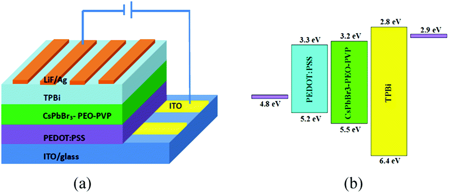 | ||
| Fig. 1 (a) The structure of device. (b) Flat-band energy level diagram of perovskite LEDs. | ||
Surface morphology and cross-sectional of perovskite thin film (CsPbBr3, CsPbBr3–PVP, CsPbBr3–PEO, CsPbBr3–PEO–PVP) was examined using a scanning electron microscope (SEM), as depicted in Fig. 2. It can be found that pure CsPbBr3 film exhibits a discontinuous surface morphology with pinholes, inhomogeneous crystals and low surface coverage (≈68% estimated using ImageJ software), which may easily lead to electrical shunt paths and leakage currents in the perovskite LED. PEO is optically transparent and electrically insulating, thus it can act as a charge-blocking material in LEDs.10 In addition, such composite films have been successfully applied as the emissive layer in CsPbBr3 PeLEDs.9,25 In order to obtain the most suitable PEO incorporation, four different CsPbBr3–PEO films with ratio of 1:0.009, 1:0.012, 1:0.018, 1:0.024 were investigated. As seen in Fig. 2(c), incorporating PEO in the CsPbBr3 solution (defined as CsPbBr3:PEO, 1:0.012 w/w ratio) leads to smaller CsPbBr3 microcrystals and high surface coverage (≈80%). As evidenced from the grain size distribution (Fig. S1a and c†), PEO restricts the growth of perovskite grains, and comparatively smaller grains can be obtained. The PEO also hinders the diffusivity of the perovskite precursor at the solvent drying stage, leading to smaller crystal size and its uniform distribution. Smaller grain suppresses the exciton quenching process that occurs at the grain boundaries.6,13,33
 | ||
| Fig. 2 The surface and cross-sectional SEM image of perovskite films on glass of (a and e) pure CsPbBr3, (b and f) CsPbBr3–PVP (1:0.06), (c and g) CsPbBr3–PEO (1:0.012), (d and h) CsPbBr3–PEO–PVP (1:0.012:0.06). | ||
Since the CsPbBr3–PEO thin films does not realize a totally pinhole-free perovskite film, the organic insulating PVP are blended into the perovskite precursor solution to improve the surface film coverage. Using the CsPbBr3:PEO film with a ratio of 1:0.012 as control condition, four different CsPbBr3:PEO:PVP film with ratio of 1:0.012:0.03, 1:0.012:0.06, 1:0.012:0.09, 1:0.012:0.012 were studied. As seen in Fig. 2(d), the CsPbBr3–PEO–PVP films with the blending ratios of 1:0.012:0.06 possess more homogeneous film morphology and higher surface coverage (≈95%) compared with those of control CsPbBr3–PEO film. Not only that, the grain size is further reduced (Fig. S1d†). In order to further explore the reasons of changes of grain size and coverage of CsPbBr3–PEO–PVP films, the SEM image of CsPbBr3–PVP films were studied. As seen in Fig. 2(b), the grain size of CsPbBr3–PVP films further decreases compared with pure CsPbBr3 films along with the addition of PVP. The coverage rate of CsPbBr3–PVP films increases from 68% to 78% (using ImageJ software) and the grain size decreases from 410 nm to 320 nm (Fig. S1†). PVP is chosen as a surfactant to control the surface coverage and morphology of the CsPbBr3 perovskite films due to its non-toxic, good film-forming properties and stability.37 It can be inferred that the perovskite films can be dispersed by PVP, and the grain size of CsPbBr3–PEO–PVP films is much smaller than that of CsPbBr3–PEO composite films and CsPbBr3 films.
In order to study the quality and crystallinity of the prepared perovskite thin film, the XRD measurements of CsPbBr3 crystals were made for all samples. The XRD patterns of pure CsPbBr3, CsPbBr3–PVP, CsPbBr3–PEO and CsPbBr3–PEO–PVP thin films are shown in Fig. 3. As shown, the XRD characteristics imparted to the CsPbBr3 crystal can be clearly observed for all samples. The diffraction peaks are at 15.2°, 21.5°, 30.4° corresponding to (001), (110), (200) plane of the perovskite crystal lattice, respectively, which are consistent with the values reported in the literature.35 It is noteworthy that with the gradual mixing of PEO and PVP, the peak strength increases and the half width decreases, which indicates that the crystallinity increases.
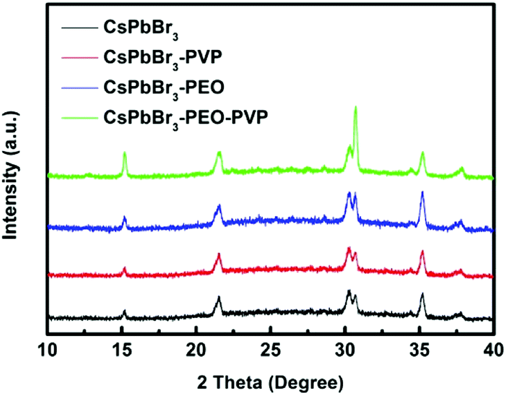 | ||
| Fig. 3 XRD patterns of the pure CsPbBr3, CsPbBr3–PEO (1:0.012), CsPbBr3–PVP (1:0.06) and CsPbBr3–PEO–PVP (1:0.012:0.06) films. | ||
The optical properties of the perovskite thin films were studied. Fig. 4(a) shows the UV-visible absorption spectra of the perovskite thin films. It can be found that no characteristic red or blue shift is observed, which confirms that the absorption of CsPbBr3 remains unchanged even when PEO and PVP are added. Fig. 4(b) presents the photoluminescence (PL) spectra of the pure CsPbBr3, CsPbBr3–PEO, CsPbBr3–PVP and CsPbBr3–PEO–PVP films. As shown, the PL intensities of the samples show a gradually increasing trend (CsPbBr3, CsPbBr3–PVP, CsPbBr3–PEO, and CsPbBr3–PEO–PVP). The additives PEO and PVP obviously increase the PL intensity without affecting its peak value. It can be seen that additives have a great impact on the crystallization of CsPbBr3 and enhance the luminescent intensity. Notably, all the films have similar UV-vis absorbance and PL spectra, and maximum peaks are all near 521 nm. It is worth noting that FWHM of PL spectra of the CsPbBr3–PEO–PVP films (21 nm) is narrower than that of the pure perovskite film (30 nm). Such enhancement is also benefited from the improved film quality and the uniformity of the perovskite thin films as regulated by the dual additive.31
 | ||
| Fig. 4 (a) UV-visible and (b) photoluminescence (PL) spectra recorded on glass pure CsPbBr3, CsPbBr3–PEO (1:0.012), CsPbBr3–PVP (1:0.06) and CsPbBr3–PEO–PVP (1:0.012:0.06) films respectively. | ||
LEDs were set up using an ITO anode/PEDOT:PSS hole-injection layer/CsPbBr3–PEO–PVP composite emissive layer/TPBi electron-injection layer/Ag cathode. The electroluminescence spectra shown in Fig. 5(a) confirm that all devices exhibit electroluminescence at 7 V with an emission wavelength of 523 nm. It is obvious that the EL intensity of CsPbBr3–PEO–PVP perovskite LED device is stronger than that of the CsPbBr3–PEO perovskite LED device and the pure CsPbBr3 perovskite LED device. Current–voltage–luminescence (J–V–L), current efficiency (CE), and external quantum efficiency (EQE) characteristics are displayed in Fig. 5. As shown in Fig. 5(b), the CsPbBr3–PEO–PVP thin film device has lower current density than the CsPbBr3 thin film device and the CsPbBr3–PEO thin film device. This may be attributed to the leakage current caused by the discontinuous CsPbBr3 film and the CsPbBr3–PEO film, which further affects device performance. The related performances of these optimized devices are summarized in Table 1. The J–V–L, current efficiency, and EQE characteristics of the LEDs based on the CsPbBr3–PEO films (1:x) with other PEO blending ratios are illustrated in Fig. S2 (ESI),† and the relevant characteristics of the devices based on the CsPbBr3–PEO–PVP films (1:0.012:x) with other PVP blending ratios are presented in Fig. S3 (ESI).† As shown, the CsPbBr3 device exhibits maximum luminance, CE, and EQE of 243 cd m−2 (at 7 V), 0.005 cd A−1 (at 6.5 V), and 0.002% (at 6.5 V), respectively. After blending proper amount of PEO, the optimized CsPbBr3–PEO (1:0.012) device achieves much enhanced device performance with maximum luminance, CE, and EQE of 1147 cd m−2 (at 6.2 V), 0.32 cd A−1 (at 6 V), and 0.15% (at 6 V). The optimized CsPbBr3–PEO–PVP (1:0.012:0.06) reaches maximum luminance, CE, and EQE of 2353 cd m−2 (at 7.2 V), 2.1 cd A−1 (at 6.5 V) and 0.85% (at 6.5 V), respectively. Fig. S4† shows the optimal brightness for three devices. Fig. S6† shows the time-dependent luminance intensities of devices based on pure CsPbBr3, CsPbBr3–PEO, and CsPbBr3–PEO–PVP emitting layers. It can be found that the operational stabilities of the devices with additives are improved because of the introduce of PEO and PVP.
 | ||
| Fig. 5 (a) Electroluminescence (EL) spectra (at 7 V), (b) J–V–L, (c) CE, (d) EQE versus voltage of the pure CsPbBr3, CsPbBr3–PEO (1:0.012), and CsPbBr3–PEO–PVP (1:0.012:0.06) devices. | ||
| Active layer | VT [V] | Lmax [cd m−2] | CEmax [cd A−1] | EQE [%] |
|---|---|---|---|---|
| CsPbBr3 | 2.8 | 243@7 V | 0.005@6.5 V | 0.002@6.5 V |
| CsPbBr3–PEO | 3 | 1147@6.2 V | 0.32@6 V | 0.15@6 V |
| CsPbBr3–PEO–PVP | 4 | 2353@7.2 V | 2.14@6.5 V | 0.85@6.5 V |
Conclusions
In summary, we have developed a simple and easy strategy to achieve smooth, complete, homogeneous, pinhole-free perovskite thin films by introducing PEO and PVP dual additives. Consequently, the optimized CsPbBr3–PEO–PVP LED obtains a maximum luminance, current efficiency, and external quantum efficiency of 2353 cd m−2 (at 7 V), 2.14 cd A−1 (at 6.5 V) and 0.85% (at 6.5 V), far surpassing the performance of the pure CsPbBr3 film device. In order to further improve performance and stability of perovskite LED device, reducing the thickness of perovskite film is worthy to be considered, and thin perovskite emitting layers is helpful for heat dissipation of the device and temperature control. Meanwhile, a dense alumina may be coated on the perovskite layer to form a dense protection, which can keep the stable device in water, air and light.38 The CsPbBr3–PEO–PVP type perovskite thin film are contributed to the improvement of performance of perovskite LEDs, which opens up a new promising avenue for future thin film LED development. It can be expected that the results will provide some help in developing polymer additive-assisted perovskite LEDs with high performance. The efficient perovskite LEDs based on the thin perovskite films will be beneficial to realizing transparent devices for the potential application in see-through displays.25Conflicts of interest
There are no conflicts to declare.Acknowledgements
This work utilized the facilities of the Institute of Semiconductor Science and Technology of South China Normal University. This work was financially supported by South China Normal University through the Perovskite Material Device Program and Start-Up Funds.References
- X. Zhang, B. Xu and J. Zhang, et al., All-Inorganic Perovskite Nanocrystals for High-Efficiency Light Emitting Diodes: Dual-Phase CsPbBr3-CsPb2Br5 Composites, Adv. Funct. Mater., 2016, 26(25), 4595–4600 CrossRef CAS.
- Z. F. Shi, X. G. Sun and D. Wu, et al., High-performance planar green light-emitting diodes based on a PEDOT:PSS/CH3NH3PbBr3/ZnO sandwich structure, Nanoscale, 2016, 8(19), 10035–10042 RSC.
- X. Dai, Z. Zhang and Y. Jin, et al., Solution-processed, high-performance light-emitting diodes based on quantum dots, Nature, 2014, 515(7525), 96 CrossRef CAS.
- J. Wang, N. Wang and Y. Jin, et al., Interfacial control toward efficient and low-voltage perovskite light-emitting diodes, Adv. Mater., 2015, 27(14), 2311–2316 CrossRef CAS.
- M. H. Park, S. H. Jeong and H. K. Seo, et al., Unravelling additive-based nanocrystal pinning for high efficiency organic-inorganic halide perovskite light-emitting diodes, Nano Energy, 2017, 42, 157–165 CrossRef CAS.
- M. Zhang, F. Yuan and W. Zhao, et al., High performance organo-lead halide perovskite light-emitting diodes via surface passivation of phenethylamine, Org. Electron., 2018, 60, 57–63 CrossRef CAS.
- N. Yantara, S. Bhaumik and F. Yan, et al., Inorganic halide perovskites for efficient light-emitting diodes, J. Phys. Chem. Lett., 2015, 6(21), 4360–4364 CrossRef CAS.
- J. Song, J. Li and X. Li, et al., Quantum dot light-emitting diodes based on inorganic perovskite cesium lead halides (CsPbX3), Adv. Mater., 2015, 27(44), 7162–7167 CrossRef CAS.
- J. Li, X. Shan and S. G. R. Bade, et al., Single-layer halide perovskite light-emitting diodes with sub-band gap turn-on voltage and high brightness, J. Phys. Chem. Lett., 2016, 7(20), 4059–4066 CrossRef CAS.
- C. Wu, Y. Zou and T. Wu, et al., Improved Performance and Stability of All-Inorganic Perovskite Light-Emitting Diodes by Antisolvent Vapor Treatment, Adv. Funct. Mater., 2017, 27(28), 1700338 CrossRef.
- Z. Wei, A. Perumal and R. Su, et al., Solution-processed highly bright and durable cesium lead halide perovskite light-emitting diodes, Nanoscale, 2016, 8(42), 18021–18026 RSC.
- L. Zhang, X. Yang and Q. Jiang, et al., Ultra-bright and highly efficient inorganic based perovskite light-emitting diodes, Nat. Commun., 2017, 8, 15640 CrossRef CAS.
- M. Y. Huang, L. Veeramuthu and C. C. Kuo, et al., Improving performance of Cs-based perovskite light-emitting diodes by dual additives consisting of polar polymer and n-type small molecule, Org. Electron., 2019, 67, 294–301 CrossRef CAS.
- L. Wu, H. Hu and Y. Xu, et al., From nonluminescent Cs4PbX6 (X = Cl, Br, I) nanocrystals to highly luminescent CsPbX3 nanocrystals: water-triggered transformation through a CsX-stripping mechanism, Nano Lett., 2017, 17(9), 5799–5804 CrossRef CAS.
- X. Li, Y. Wu and S. Zhang, et al., CsPbX3 quantum dots for lighting and displays: room-temperature synthesis, photoluminescence superiorities, underlying origins and white light-emitting diodes, Adv. Funct. Mater., 2016, 26(15), 2435–2445 CrossRef CAS.
- L. Zhang, X. Yang and Q. Jiang, et al., Ultra-bright and highly efficient inorganic based perovskite light-emitting diodes, Nat. Commun., 2017, 8, 15640 CrossRef CAS.
- X. Ji, X. Peng and Q. Wang, et al., On the performance of polymer: organometal halide perovskite composite light emitting devices: The effects of polymer additives, Org. Electron., 2018, 52, 350–355 CrossRef CAS.
- Y. L. Shi, F. Liang and Y. Hu, et al., High-efficiency quantum dot light-emitting diodes employing lithium salt doped poly (9-vinlycarbazole) as a hole-transporting layer, J. Mater. Chem. C, 2017, 5(22), 5372–5377 RSC.
- J. C. Germino, E. Yassitepe, J. N. Freitas, et al., Color tunable hybrid light-emitting diodes based on perovskite quantum dot/conjugated polymer, Organic, Hybrid, and Perovskite Photovoltaics XVIII, International Society for Optics and Photonics, 2017, vol. 10363, p. 103630Q Search PubMed.
- P. Chen, Z. Xiong and X. Wu, et al., Highly efficient perovskite light-emitting diodes incorporating full film coverage and bipolar charge injection, J. Phys. Chem. Lett., 2017, 8(8), 1810–1818 CrossRef CAS PubMed.
- G. Li, Z. K. Tan and D. Di, et al., Efficient light-emitting diodes based on nanocrystalline perovskite in a dielectric polymer matrix, Nano Lett., 2015, 15(4), 2640–2644 CrossRef CAS.
- K. Ma, X. Y. Du and Y. W. Zhang, et al., In situ fabrication of halide perovskite nanocrystals embedded in polymer composites via microfluidic spinning microreactors, J. Mater. Chem. C, 2017, 5(36), 9398–9404 RSC.
- S. Kumar, J. Jagielski and N. Kallikounis, et al., Ultrapure green light-emitting diodes using two-dimensional formamidinium perovskites: Achieving recommendation 2020 color coordinates, Nano Lett., 2017, 17(9), 5277–5284 CrossRef CAS.
- W. Ruan, Y. Hu and T. Qiu, et al., Morphological regulation of all-inorganic perovskites for multilevel resistive switching, J. Phys. Chem. Solids, 2019, 127, 258–264 CrossRef CAS.
- L. Song, X. Guo and Y. Hu, et al., Efficient inorganic perovskite light-emitting diodes with polyethylene glycol passivated ultrathin CsPbBr3 films, J. Phys. Chem. Lett., 2017, 8(17), 4148–4154 CrossRef CAS.
- S. G. R. Bade, J. Li and X. Shan, et al., Fully printed halide perovskite light-emitting diodes with silver nanowire electrodes, ACS Nano, 2015, 10(2), 1795–1801 CrossRef PubMed.
- J. Wang, N. Wang and Y. Jin, et al., Interfacial control toward efficient and low-voltage perovskite light-emitting diodes, Adv. Mater., 2015, 27(14), 2311–2316 CrossRef CAS.
- Q. Dong, Z. Wang and K. Zhang, et al., Easily accessible polymer additives for tuning the crystal-growth of perovskite thin-films for highly efficient solar cells, Nanoscale, 2016, 8(10), 5552–5558 RSC.
- Z. Wei, A. Perumal and R. Su, et al., Solution-processed highly bright and durable cesium lead halide perovskite light-emitting diodes, Nanoscale, 2016, 8(42), 18021–18026 RSC.
- H. Huang, F. Zhao and L. Liu, et al., Emulsion synthesis of size-tunable CH3NH3PbBr3 quantum dots: an alternative route toward efficient light-emitting diodes, ACS Appl. Mater. Interfaces, 2015, 7(51), 28128–28133 CrossRef CAS.
- M. Xue, H. Zhou and G. Ma, et al., Investigation of the stability for self-powered CsPbBr3 perovskite photodetector with an all-inorganic structure, Sol. Energy Mater. Sol. Cells, 2018, 187, 69–75 CrossRef CAS.
- Y. F. Ng, W. J. Neo and N. F. Jamaludin, et al., Enhanced Coverage of All-Inorganic Perovskite CsPbBr3 through Sequential Deposition for Green Light-Emitting Diodes, Energy Technol., 2017, 5(10), 1859–1865 CrossRef CAS.
- X. Ji, X. Peng and Y. Lei, et al., Multilayer light emitting devices with organometal halide perovskite: Polymer composite emission layer: The relationship of device performance with the compositions of emission layer and device configurations, Org. Electron., 2017, 43, 167–174 CrossRef CAS.
- Y. Ling, Y. Tian and X. Wang, et al., Enhanced Optical and Electrical Properties of Polymer-Assisted All-Inorganic Perovskites for Light-Emitting Diodes, Adv. Mater., 2016, 28(40), 8983–8989 CrossRef CAS.
- K. Lin, J. Xing and L. N. Quan, et al., Perovskite light-emitting diodes with external quantum efficiency exceeding 20 per cent, Nature, 2018, 562(7726), 245–248 CrossRef CAS PubMed.
- Y. Shi, W. Wu and H. Dong, et al., A Strategy for Architecture Design of Crystalline Perovskite Light-Emitting Diodes with High Performance, Adv. Mater., 2018, 1800251 CrossRef.
- Y. Ding, X. Yao and X. Zhang, et al., Surfactant enhanced surface coverage of CH3NH3PbI3-xClx perovskite for highly efficient mesoscopic solar cells, J. Power Sources, 2014, 272, 351–355 CrossRef CAS.
- A. Loiudice, S. Saris and E. Oveisi, et al., CsPbBr3 QD/AlOx Inorganic Nanocomposites with Exceptional Stability in Water, Light, and Heat, Angew. Chem., 2017, 129, 10836–10841 CrossRef.
- L. Zhang, X. Yang and Q. Jiang, et al., Ultra-bright and highly efficient inorganic based perovskite light-emitting diodes, Nat. Commun., 2017, 8, 15640 CrossRef CAS.
Footnote |
| † Electronic supplementary information (ESI) available. See DOI: 10.1039/c9ra05053a |
| This journal is © The Royal Society of Chemistry 2019 |