
 Open Access Article
 This Open Access Article is licensed under a Creative Commons Attribution-Non Commercial 3.0 Unported Licence
High efficiency Mg2(Si,Sn)-based thermoelectric materials: scale-up synthesis, functional homogeneity, and thermal stability†
Nader Farahi *a,
Christian Stiewea,
D. Y. Nhi Truonga,
Johannes de Boora and
Eckhard Müllerab
*a,
Christian Stiewea,
D. Y. Nhi Truonga,
Johannes de Boora and
Eckhard Müllerab
aInstitute of Materials Research, German Aerospace Center (DLR), D-51170 Köln, Germany. E-mail: nfarahi@uwaterloo.ca
bInstitute of Inorganic and Analytical Chemistry, Justus Liebig University Gießen, D-35392 Gießen, Germany
First published on 25th July 2019
Abstract
Considering the need for large quantities of high efficiency thermoelectric materials for industrial applications, a scalable synthesis method for high performance magnesium silicide based materials is proposed. The synthesis procedure consists of a melting step followed by high energy ball milling. All the materials synthesized via this method demonstrated not only high functional homogeneity but also high electrical conductivity and Seebeck coefficients of around 1000 Ω−1 cm−1 and −200 μV K−1 at 773 K, respectively. The measured values were similar for all the samples extracted from the ∅50 mm and ∅70 mm compacted pellets and were stable upon thermal cycling. Thermal stability experiments from 168 hours to 720 hours at 723 K revealed no significant change in the material properties. The low thermal conductivity of ∼2.5 W m−1 K−1 at 773 K led to a maximum figure of merit, zTmax, of 1.3 at the same temperature and an average value, zTavg, of 0.9 between 300 K and 773 K, which enables high efficiency in future silicide-based thermoelectric generators.
1. Introduction
Contemplating the decades of space exploration missions, thermoelectric (TE) materials are auspiciously established as a unique energy supplier for space explorers such as Cassini, the Voyager probes, and most recent Mars rover Curiosity.1,2 Moreover, this notable capacity is not limited to the space program, and also TE materials are now on the verge of waste heat recovery for stationary3 and non-stationary4,5 applications. In order to alleviate the destructive impact of climate change on our planet, both CO2 emission and fossil fuel consumption need to be reduced. Therefore, it is vital to recuperate as much waste heat as possible. In that context, TE materials, which are made of cost effective, environmentally benign elements, and have high efficiency, are inimitable.6 The criterion to evaluate the efficiency of a TE material is called figure of merit, z, which is commonly defined in its dimensionless form through zT = S2σ(κph + κe)−1T, where S, σ, κph, κe, and T represent Seebeck coefficient, electrical conductivity, lattice thermal conductivity, electronic thermal conductivity, and absolute temperature, respectively.7Magnesium silicide based TE materials are worth investigating as potential candidates for module fabrication due to fulfilling most of the above-mentioned criteria. Mg2Si adopts an anti-fluorite cubic structure which belongs to the high symmetry Fm![[3 with combining macron]](https://www.rsc.org/images/entities/char_0033_0304.gif) m space group with a band gap of ∼0.77 eV.8 The combination of low intrinsic carrier concentration (∼3 × 1017 cm−3 at 300 K) and a high symmetry structure consisting of light atoms with strong covalent bonds manifests itself in low electrical conductivity (∼2 Ω−1 cm−1 at 300 K) and high thermal conductivity (∼10 W m−1 K−1 at 300 K) leading to a zT of below 0.1 at 300 K, which does not significantly enhance even at high temperature.9,10 Increasing the electrical conductivity can be achieved via increasing the carrier density through doping with non-isoelectronic elements. So far, for n-type doping, group XV elements such as bismuth (Bi)11–18 and antimony (Sb),19–25 which replace silicon (Si), appear to be the most potent in enhancing the carrier concentration (more than 1020 cm−3 at 300 K); therefore, increasing the electrical conductivity.16 Reducing the thermal conductivity is also attainable by reducing the lattice contribution (κph) via phonon scattering. To enhance this scattering effect, alloying with both heavier and larger isoelectronic atoms, such as germanium (Ge)26–28 and tin (Sn)29–32 on the Si position, have demonstrated to efficaciously reduce the thermal conductivity by 70% as compared to its non-alloyed value (from ∼10 W m−1 K−1 to ∼2.5 W m−1 K−1).10,17 In order to reach lattice thermal conductivity values close to the alloy limit, phonons with a wide range of wavelengths need to be scattered via integrating other strategies, such as nanostructuring,33–36 nano-inclusion,10,37–39 and modulation doping,40 with alloying. The best performing materials in the Mg2(Si,Sn) system usually contain ∼23 ± 3 at% Sn, which is where the conduction band convergence is taking place,41,42 and all exhibit a maximum figure of merit, zTmax, of 1.4 ± 0.2, satisfactory for the device applications.43
m space group with a band gap of ∼0.77 eV.8 The combination of low intrinsic carrier concentration (∼3 × 1017 cm−3 at 300 K) and a high symmetry structure consisting of light atoms with strong covalent bonds manifests itself in low electrical conductivity (∼2 Ω−1 cm−1 at 300 K) and high thermal conductivity (∼10 W m−1 K−1 at 300 K) leading to a zT of below 0.1 at 300 K, which does not significantly enhance even at high temperature.9,10 Increasing the electrical conductivity can be achieved via increasing the carrier density through doping with non-isoelectronic elements. So far, for n-type doping, group XV elements such as bismuth (Bi)11–18 and antimony (Sb),19–25 which replace silicon (Si), appear to be the most potent in enhancing the carrier concentration (more than 1020 cm−3 at 300 K); therefore, increasing the electrical conductivity.16 Reducing the thermal conductivity is also attainable by reducing the lattice contribution (κph) via phonon scattering. To enhance this scattering effect, alloying with both heavier and larger isoelectronic atoms, such as germanium (Ge)26–28 and tin (Sn)29–32 on the Si position, have demonstrated to efficaciously reduce the thermal conductivity by 70% as compared to its non-alloyed value (from ∼10 W m−1 K−1 to ∼2.5 W m−1 K−1).10,17 In order to reach lattice thermal conductivity values close to the alloy limit, phonons with a wide range of wavelengths need to be scattered via integrating other strategies, such as nanostructuring,33–36 nano-inclusion,10,37–39 and modulation doping,40 with alloying. The best performing materials in the Mg2(Si,Sn) system usually contain ∼23 ± 3 at% Sn, which is where the conduction band convergence is taking place,41,42 and all exhibit a maximum figure of merit, zTmax, of 1.4 ± 0.2, satisfactory for the device applications.43
As for industrial applications, in addition to the electrode development which is in good progress,44–46 a large amount of material is required; thus, a scalable synthesis method that sustains the outstanding TE properties of the material needs to be established. The up-scaling process can be challenging due to occurrence of de-mixing phenomena such as the formation of Si-rich and Sn-rich regions induced by gravity.47 Moreover, with respect to the larger amount of Mg and longer processing time, controlling the evaporation of Mg could be problematic. Although a previous study showed that the Mg loss in an up-scaling process can be tackled utilizing the gas atomization technique,48 this method is not commonly available in material synthesis laboratories. In this study, a practical scalable procedure for synthesis of high efficiency Bi-doped Mg2(Si,Sn) based TE materials together with the effect of heat treatment on the microstructure and TE properties of these materials will be discussed. The proposed procedure comprises less steps and shorter duration compared to the conventional solid state reaction which was employed for large scale Bi-doped Mg2Si production,49 and the samples demonstrate higher structural stability than those of up-scaled Bi-doped and Sb-doped Mg2Si0.4Sn0.6 upon thermal cycling.50 Although this study focuses on the high performance n-type material, we believe the technique can be applied to this class of material with different doping or Si/Sn ratio (Fig. S1†) with subtle adjustments, and is a step forward towards the technological feasibility of silicide based thermoelectric generators (TEGs).
2. Experimental section
Mg2Si0.3Sn0.675Bi0.025 samples were prepared by using Mg pellets (99.99%, Evochem, 3–6 mm), Si powder (99.9%, Alfa Aesar, −100 mesh), Sn granules (99.99%, Evochem, 1–4 mm), and Bi granules (99.999%, Goodfellow, ∼7 mm) for the synthesis. The elements were placed inside a graphite crucible in an argon filled glove box according to the stoichiometric ratios plus ∼6 wt% of excess Mg to compensate for the evaporation during high temperature steps of the material preparation. The crucible was then transferred to a Direct-Current Sintering Press (Dr. Fritsch GmbH, DSP 510 SE) for the melting process. Subsequently, melting was performed at various temperatures (from 973 K to 1273 K) for three times consecutively to increase stoichiometric homogeneity. To complete the reaction and facilitate the homogenization process, the obtained ingot was then ball-milled for around 12 hours using a high-energy SPEX Sample Prep 8000D Mixer Mill with stainless steel balls and vials, where the weight of the collected powder is more than 98% of the targeted initial mass. To obtain compacted pellets, the as-milled powder was sintered at 973 K for 20 minutes under ∼40–60 MPa and partial Ar atmosphere using DSP 510 SE with graphite dies of 50 mm and 70 mm inner diameter, respectively. To alleviate strain and stress on the pellets, the pressure was released during their natural cooling process.A D8 Discover Bruker X-ray diffractometer with Cu-Kα1 radiation and a HI-STAR-2D area detector was used to determine the purity of the synthesized samples. X-ray patterns on the pellets (Fig. S2†) revealed small traces of Mg from the excess amount used, and magnesium oxide (MgO) which is a well-known side product in Mg2Si based compounds.51–53
The pressed pellets were 50 mm and 70 mm in diameter and ∼5 mm in thickness. The functional homogeneity of the pellets was investigated by an in-house developed surface scanning Seebeck microprobe (PSM).54 For measuring the electrical conductivity (σ) and Seebeck coefficient (S), the pressed pellets were subsequently cut into bars with the dimensions of approximately 10 × 10 × 4 mm. The measurements were carried out under helium (He) atmosphere between 300 K and 773 K by utilizing an in-house developed facility (High Temperature Seebeck and Sigma Measurement Instrument) applying a four-probe method.55 The detailed analysis of the Seebeck coefficient measurement is explained elsewhere;56 the uncertainty of the measurement can arise from various sources such as cold finger effect57 and is estimated to be around 5%.58 To study the effect of heat treatment on the microstructure of the samples, scanning electron microscopy (SEM) analysis was performed on parts of pellets using an ULTRA 55 electron microscope equipped with a Zeiss QBSE detector associated with an Oxford energy dispersive X-ray (EDX) device, EDAX PentaFETx3.
Thermal diffusivity (α) of the pressed pellets was measured between 300 K and 773 K under Ar flow using the laser flash Netzsch LFA 427 apparatus. The measured values were then multiplied by the density (ρ) of the pellets, measured via the Archimedes method in ethanol, and the specific heat (Cp) of the compounds, calculated utilizing the Dulong–Petit approximation, to obtain the thermal conductivity (κ), κ = α × ρ × Cp. The calculated specific heat together with the obtained densities of all the samples is available in Tables S1 and S2.† The Dulong–Petit approximation was previously confirmed to be well within the accepted accuracy for Mg2Si based materials.26,59
Thermal stability experiments were performed on boron nitride coated samples under partial Ar pressure using a GERO-D7531 vertical resistance heater furnace. The annealing temperature was fixed at 723 K and the test duration varied between 168 hours and 720 hours.
3. Results and discussion
First of all, it is worth to mention that the initial attempts on large scale synthesis of high performance Mg2(Si,Sn) materials led to a clear agglomeration of Sn and Sn-rich phases at the bottom of the compacted pellet (Fig. S3†). This could be due to the current passing through the sample during sintering which softened the heavier Sn-rich phases with low melting points. As a consequence, these compositions accumulate at the bottom of the as-sintered pellet. To tackle this issue, the current path through the sample is blocked through non-conductive coating and a gradual heating procedure is then employed for the sintering process. The surface Seebeck scan of both surfaces together with the cross section of the ∅50 mm pellet made by pressing 50 grams of Mg2Si0.3Sn0.675Bi0.025 powder is shown in Fig. 1.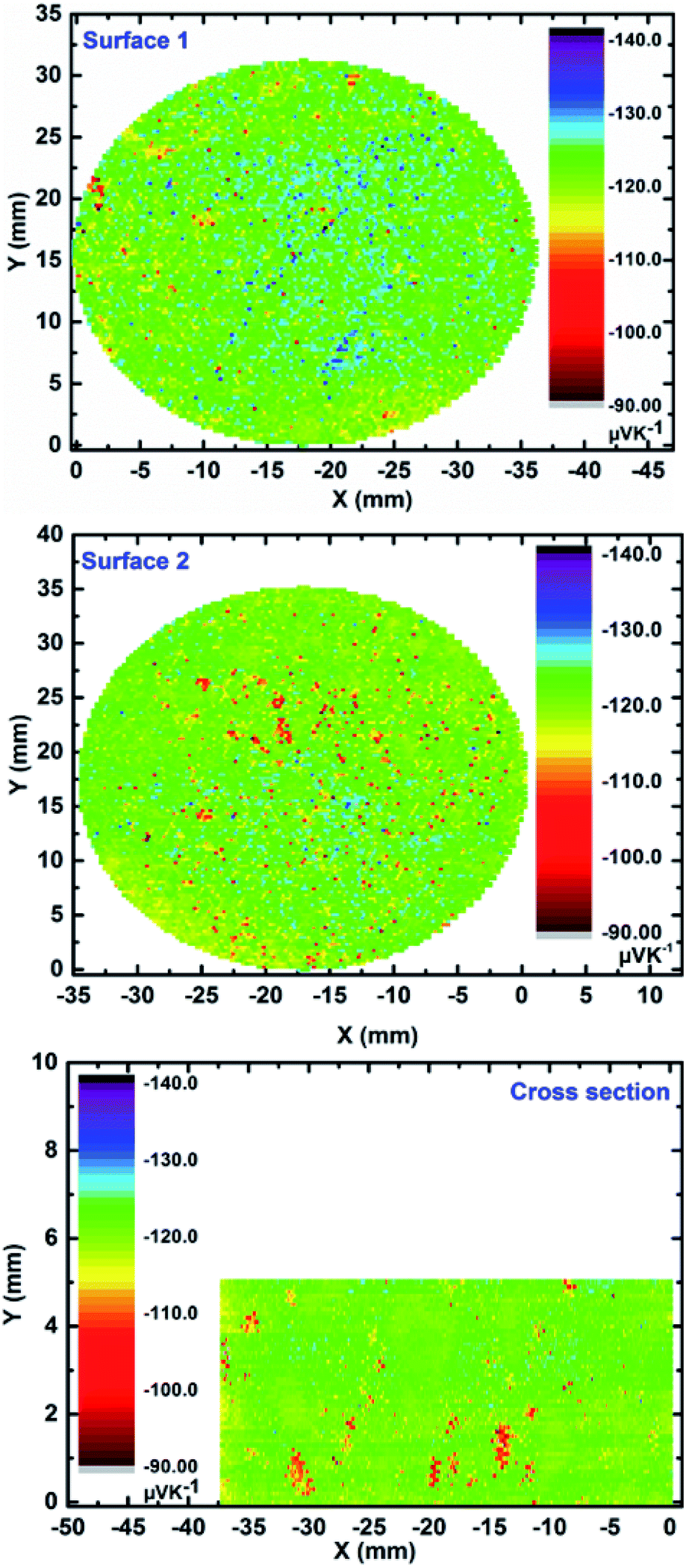 | ||
| Fig. 1 Surface Seebeck scans of both base faces and cross section of ∅50 mm Mg2Si0.3Sn0.675Bi0.025 pellet compacted from 50 grams of material (error 5%). | ||
The negative values of the Seebeck coefficient on all the surfaces confirm electrons to be the major charge carriers, as expected due to bismuth doping on the silicon position. All the surfaces exhibit high functional homogeneity with the average Seebeck value of −122 ± 7 μV K−1 in majority of the areas. The obtained average value is well within the range of previously reported Bi-doped Mg2(Si,Sn) samples with the optimized doping level.15,17 As an example, the frequency count of Seebeck values for one of the surfaces is illustrated in Fig. S4† demonstrating mainly a single peak distribution behaviour. Moreover, the scanning electron image together with the compositional EDX analysis along the cross section of the sample (Fig. S5†) show rather uniform compositions close to the nominal values (Mg ∼ 66.7 at%, Si ∼ 10.0 at%, Sn ∼ 22.5 at%, Bi ∼ 0.8 at%). For the transport property measurements, the ∅50 mm sample was divided into quarters (numbered as I–IV) and one sample from each quarter was extracted to assure and confirm the consistency of the observed values. Fig. 2 shows the temperature dependent Seebeck coefficient of all samples in one heating and cooling cycle from ∼300 K to ∼773 K. The average Seebeck value of all samples at ∼300 K is around −115 ± 6 μV K−1 which is in good agreement with the value obtained from surface Seebeck measurement on the whole pellet. This value is in the expected range for the heavily doped n-type Mg2(Si,Sn) compounds due to the high carrier concentration in the order of 1020 cm−3.17,23,43 By increasing the temperature, the absolute Seebeck value is increased for all the samples and reached an average maximum value of −200 ± 10 μV K−1 at ∼773 K.
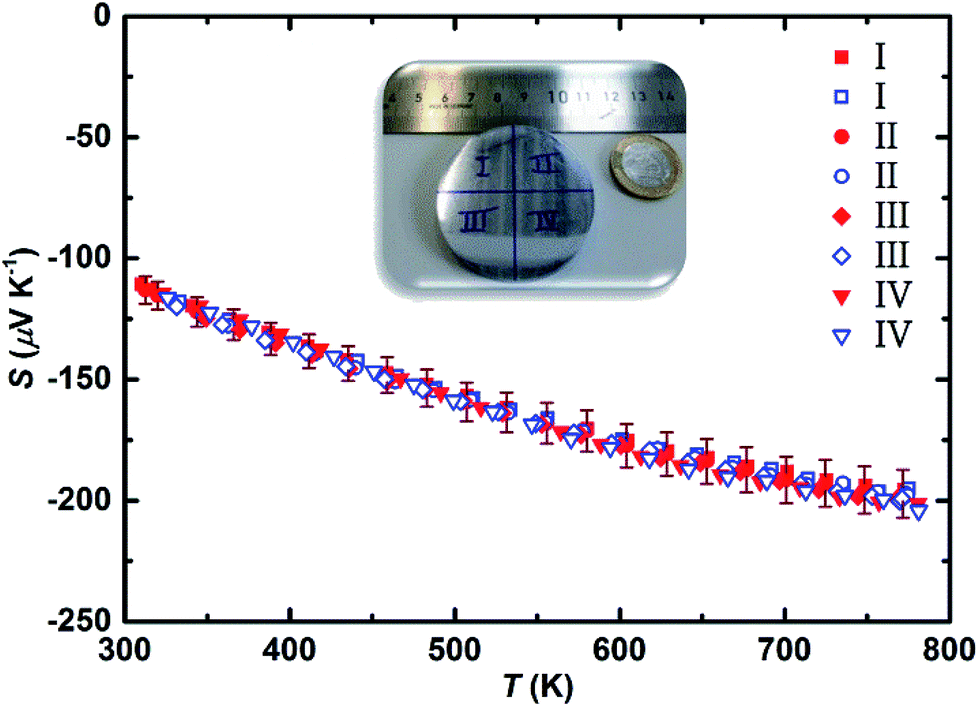 | ||
| Fig. 2 Seebeck coefficient of the four samples extracted from the ∅50 mm Mg2Si0.3Sn0.675Bi0.025 pellet (I–IV) (error 5%). The solid and open symbols represent the heating and cooling cycles, respectively. | ||
The electrical conductivity of all the samples is presented in Fig. 3. All samples exhibit fairly similar (within the uncertainty range of the measurement) electrical conductivity of above 2000 Ω−1 cm−1 at ∼300 K that proves their heavily doped character compared to ∼2 Ω−1 cm−1 at ∼300 K for an undoped material.10 All samples follow the degenerate semiconductor behavior with increasing the temperature, and their electrical conductivity decreases due to a decrease in mobility.60 Even though magnesium oxide can reduce the electrical conductivity at lower temperatures,53 we only observed the usual decrease with elevated temperature due to the scattering of electrons with acoustic phonons, indicating that the detected MgO amount does not significantly influence the thermoelectric properties. All samples reach a value of around 1000 Ω−1 cm−1 at ∼773 K which is quite comparable with the values previously reported for Bi-doped Mg2(Si,Sn) with similar composition.15,17,43 Although the Seebeck values of these samples are similar to those of the Mg2Si0.5875Sn0.4Sb0.0125 samples synthesized using gas atomization technique,48 the initial electrical conductivities (∼2500 Ω−1 cm−1) are around 25% higher, which could be attributed to both higher doping level (higher carrier concentration) and optimum Sn content leading to less alloy scattering (i.e. higher carrier mobility).
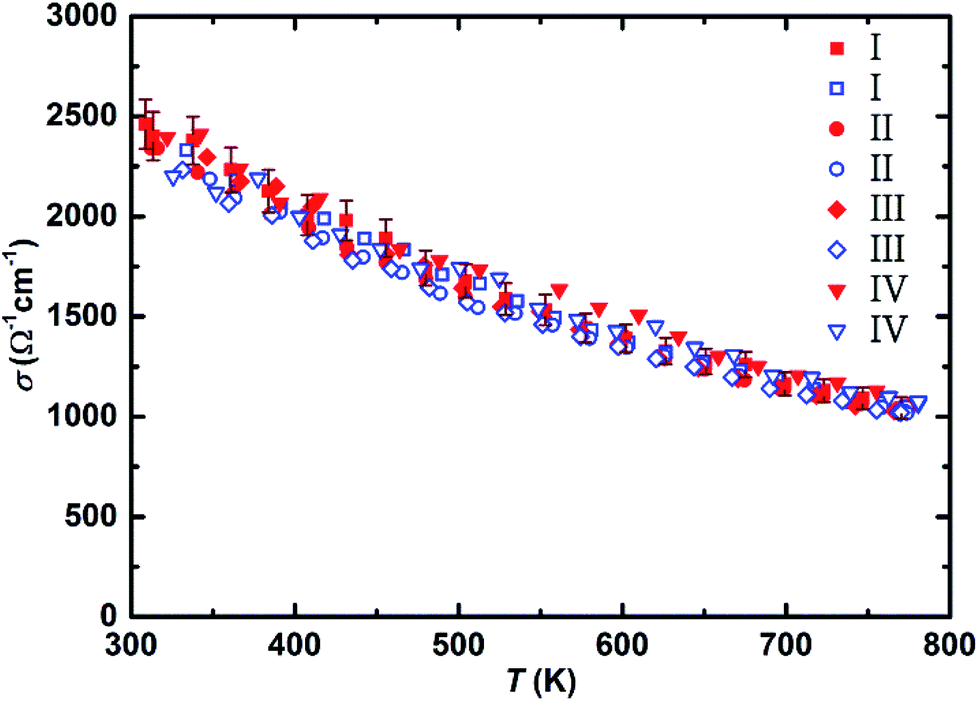 | ||
| Fig. 3 Electrical conductivity of the four samples extracted from the ∅50 mm Mg2Si0.3Sn0.675Bi0.025 pellet (I–IV) (error 5%). The solid and open symbols represent the heating and cooling cycles, respectively. | ||
To be able to calculate the dimensionless figure of merit (zT) for all the samples, the thermal conductivity of sample number I is measured and used for the calculation. Since all the samples have the same chemical composition and manifest rather identical electrical conductivity, Seebeck coefficient, and density values, no significant difference is expected for their thermal conductivity.
Fig. 4 shows the temperature dependent total thermal conductivity together with the lattice and bipolar contributions of the thermal conductivity of sample I. The thermal conductivity decreases from 2.82 W m−1 K−1 at ∼350 K to reach a minimum value of 2.35 W m−1 K−1 at ∼700 K. For the temperature above 700 K, a slight increase in thermal conductivity is observed which is due to the excitation of intrinsic carriers (bipolar contribution) leading to a value of 2.47 W m−1 K−1 at ∼773 K. The obtained values are very well comparable with the previously reported ones for Mg2Si0.3Sn0.7−xBix composition.17 The Mg2Si0.5875Sn0.4Sb0.0125 sample synthesized using gas atomization showed slightly lower thermal conductivity at high temperatures (>700 K), which could be due to more alloy scattering (less Sn substitutions), less bipolar contribution (larger band gap originating from lower Sn content), and smaller grain sizes.48
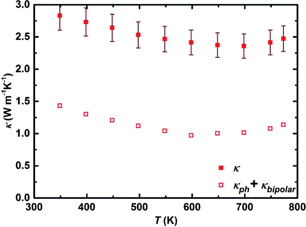 | ||
| Fig. 4 Total thermal conductivity (solid symbols), lattice and bipolar thermal conductivity (open symbols) of sample I (error 8%). | ||
The lattice and bipolar contributions to the thermal conductivity, κph + κbipolar, were extracted from the total thermal conductivity (Fig. 4), κ, by deducting the electronic part of the thermal conductivity, κe, which was calculated employing the Wiedemann–Franz law, κe = L × σ × T. To calculate κe, the temperature dependence of the Lorenz number, L, was obtained through the L (10−8 V2 K−2) = 1.5 + exp[−|S|/116 μV K−1] equation, where S is in μV K−1, and L is expressed in 10−8 V2 K−2. Assuming the validity of a single parabolic band model and elastic carrier scattering, the obtained Lorenz number values are within 5% accuracy and in good agreement with the previously reported values for the Mg2(Si,Sn) system.17,61 The lattice thermal conductivity of 1.4 W m−1 K−1 and 1.1 W m−1 K−1 at ∼350 K and ∼773 K, respectively, indicates that nearly half of the total thermal conductivity is carried by phonons. To further reduce the thermal conductivity, it is worthwhile to examine approaches that affect phonon scattering by extended structural defects such as grain boundary engineering,62,63 mesostructuring,64 and hierarchical architectures.65 The dimensionless figure of merit, zT, of all samples in the temperature range of 300 K to 800 K is presented in Fig. 5. The figure of merit of all samples starts from around 0.3 at ∼300 K and enhances with increasing temperature to around 1.3 at ∼773 K, that is quite comparable to the as-synthesized sample using gas atomization method and among the highest so far reported efficiency for this class of material.12,15,17,23,66 This provides an average zT of 0.9 over the whole temperature range which is distinctly beneficial from the module fabrication point of view. The figure of merit of all samples is within the accepted uncertainty range of calculation (10–20%).67
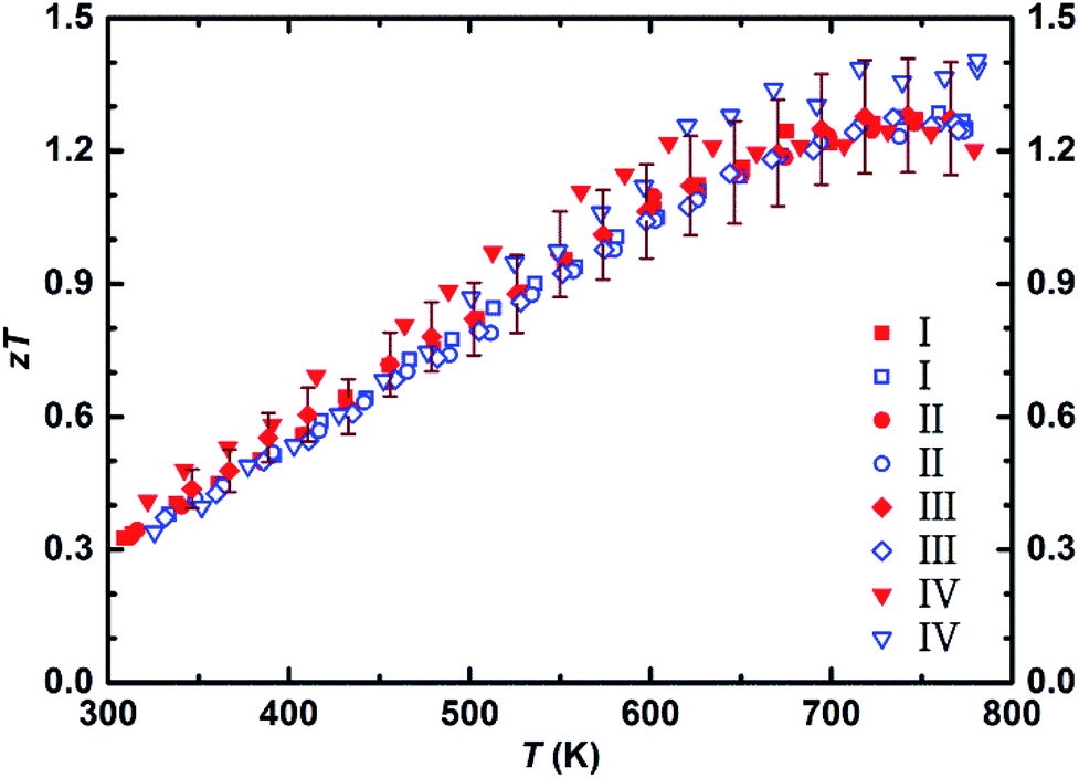 | ||
| Fig. 5 Temperature dependent dimensionless figure of merit of four samples extracted from the ∅50 mm Mg2Si0.3Sn0.675Bi0.025 pellet (I–IV) (error 10%). | ||
In another attempt to expand the scalability of this method, 75 grams of the material synthesized through a similar procedure was pressed using the ∅70 mm graphite die. The X-ray diffraction analysis made on 10 different points on the sample (Fig. S6†) reveals similar phase homogeneity to what was achieved for the ∅50 mm pellet. The comparison between the electronic transport properties of 50 gram and 75 gram sample is illustrated in Fig. 6. Across the entire temperature range, both electrical conductivity and Seebeck coefficient values can be considered analogous within the accepted uncertainty of the measurement.
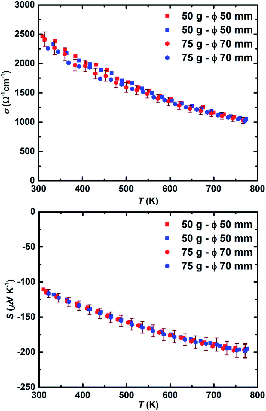 | ||
| Fig. 6 Electrical conductivity (top) and Seebeck coefficient (bottom) of the samples extracted from the ∅50 mm and ∅70 mm Mg2Si0.3Sn0.675Bi0.025 pellets (error 5%, red and blue symbols represent heating and cooling cycles, respectively). | ||
To be able to employ the high efficiency of the synthesized material for module fabrication, it is crucial to have knowledge concerning the thermal stability of the material. For this purpose, three samples (numbered I to III) were extracted from the ∅70 mm pellet and annealed at 723 K (i.e. operational temperature at the hot side of Mg2(Si,Sn) based thermoelectric module) for the durations of 168 hours, 336 hours, and 720 hours, respectively. Fig. 7 shows the electrical conductivity and Seebeck coefficient of the samples before and after heat treatment. Since MgO formation was previously observed on the samples heat treated in air,68–70 partial Ar atmosphere was chosen for our experiments.
 | ||
| Fig. 7 Electrical conductivity (top) and Seebeck coefficient (bottom) of the samples extracted from the ∅70 mm pellets before (solid symbols) and after (open symbols) heat treatment (error 5%, red and blue symbols represent heating and cooling cycles, respectively). | ||
Boron nitride (BN) coating was shown earlier to be a potent high temperature coating for Mg2Si0.3Sn0.7 sample in order to prevent Mg loss and oxidation;71 therefore, it is also applied to our samples. Table S3† summarizes the electronic transport properties of all the samples before and after heat treatment at ∼773 K. No significant change is observed in any of those properties, corroborating the stability of the synthesized material under the examined conditions. To be able to successfully operate the Mg2(Si,Sn) based devices in air, an anti-oxidation layer needs to be developed covering the materials' exposed surfaces. For instance, yttria-stabilized zirconia ((Y2O3)0.08(ZrO2)0.92, YSZ) appeared to be an effective anti-oxidation barrier for Mg2Si legs heat treated at 973 K in air, which hampered the oxygen diffusion without significantly affecting the electrode contact resistance.72 Hence, it is worth to investigate later the effect of yttria-stabilized zirconia coating on the high efficiency Mg2(Si,Sn) based legs. Although a slight decrease in electrical conductivity and a small increase in Seebeck coefficient observed after 720 hours of annealing, this could also be partly attributed to the grain growth detected on the SEM image of the sample before and after heat treatment (Fig. S7†). However, it should be noted that these changes are still within the error ranges of the measurements meaning the materials remain functionally stable after this long period of heat treatments.
All in all, the materials obtained from this scalable synthesis route not only show a high performance zT reaching around 1.3 at 773 K, but also are scalable and stable under heat treatment up to 720 hours. To the best of our knowledge, there are very few reported works on the successful large scale synthesis of high efficiency magnesium silicide-based compounds; aside from our method, the other approaches include gas atomization48 and solid state reaction.50 On the one hand, the gas atomization was successful in producing large quantities of material with high performance (zTmax ∼ 1.4 at 800 K), but the apparatus is not easily accessible and operable in usual material science laboratories. On the other hand, the solid state reaction was used to make around 100 grams of sample in one batch. Unfortunately, the synthesized materials show a low thermal stability and performance (zTmax ∼ 0.28 at 650 K) due to the Sn-rich phase segregation.50 Here, our method has proven its advantages of producing batches up to 100 grams of high performance materials by means of easily accessible and operable apparatus. Even though this achievement is a great starting point for silicide based module fabrication, further studies such as applying temperature gradients on the pellets and annealing beyond 720 hours are indispensable.
4. Conclusions
Large scale high efficiency Mg2Si0.3Sn0.675Bi0.025 samples were successfully synthesized utilizing the combination of melting and ball milling techniques. By this synthesis route a high functional homogeneity is achieved on the surfaces and cross section of the pellets. All samples exhibited heavily doped semiconducting character with the electrical conductivity of above 2000 Ω−1 cm−1 at room temperature. The Seebeck coefficient of all the samples culminated around −200 μV K−1 at 773 K. The effect of heat treatment on the thermoelectric properties of the prepared samples verified the stability of the TE material for at least 720 hours at 723 K. Lastly, all the samples attained a maximum zT of approximately 1.3 at 773 K, which is among the highest hitherto proclaimed for Mg2Si1−xSnx based thermoelectric materials. Subsequently, fabricating larger scales and different compositions as well as understanding the effect of temperature gradient on the microstructure and TE properties of these materials can be explored.Conflicts of interest
The authors declare no conflict of interest.Acknowledgements
The authors would like to kindly acknowledge the support from the endorsement from the DLR Executive Board Member for Space Research and Technology and the financial support from the Young Research Group Leader Program. We would also like to thank P. Blaschkewitz and P. Ziolkowski for their support with the thermoelectric measurements. N. F would like to thank DAAD for financial support through DLR-DAAD Fellowship Program No. 248.References
- R. R. Furlong and E. J. Wahlquist, Nucl. News, 1999, 42, 26–35 Search PubMed.
- G. Schmidt, L. Dudzinski and T. Sutliff, in 6th International Energy Conversion Engineering Conference (IECEC), Ohio, United States of America, 2011, p. 5640 Search PubMed.
- L. I. Anatychuk, Y. Y. Rozver and D. D. Velichuk, J. Electron. Mater., 2011, 40, 1206–1208 CrossRef CAS.
- J. Yang and F. R. Stabler, J. Electron. Mater., 2009, 38, 1245–1251 CrossRef CAS.
- Y. Wang, L. Yang, X.-L. Shi, X. Shi, L. Chen, M. S. Dargusch, J. Zou and Z.-G. Chen, Adv. Mater., 2019, 31, 1807916 CrossRef PubMed.
- W.-D. Liu, Z.-G. Chen and J. Zou, Adv. Energy Mater., 2018, 8, 1800056 CrossRef.
- A. F. Ioffe, Physics of Semiconductors, Infosearch, New York City, NY, 1960 Search PubMed.
- G. Busch and U. Winkler, Physica, 1954, 20, 1067–1072 CrossRef CAS.
- M. Akasaka, T. Iida, A. Matsumoto, K. Yamanaka, Y. Takanashi, T. Imai and N. Hamada, J. Appl. Phys., 2008, 104, 013703 CrossRef.
- D. Cederkrantz, N. Farahi, K. A. Borup, B. B. Iversen, M. Nygren and A. E. C. Palmqvist, J. Appl. Phys., 2012, 111, 23701 CrossRef.
- T. Sakamoto, T. Iida, A. Matsumoto, Y. Honda, T. Nemoto, J. Sato, T. Nakajima, H. Taguchi and Y. Takanashi, J. Electron. Mater., 2010, 39, 1708–1713 CrossRef CAS.
- A. U. Khan, N. V Vlachos, E. Hatzikraniotis, G. S. Polymeris, C. B. Lioutas, E. C. Stefanaki, K. M. Paraskevopoulos, I. Giapintzakis and T. Kyratsi, Acta Mater., 2014, 77, 43–53 CrossRef CAS.
- A. U. Khan, N. Vlachos and T. Kyratsi, Scr. Mater., 2013, 69, 606–609 CrossRef CAS.
- J. Tani and H. Kido, Phys. B, 2005, 364, 218–224 CrossRef CAS.
- W. Liu, Q. Zhang, K. Yin, H. Chi, X. Zhou, X. Tang and C. Uher, J. Solid State Chem., 2013, 203, 333–339 CrossRef CAS.
- N. Farahi, M. VanZant, J. Zhao, J. S. Tse, S. Prabhudev, G. A. Botton, J. R. Salvador, F. Borondics, Z. Liu and H. Kleinke, Dalton Trans., 2014, 43, 14983–14991 RSC.
- N. Farahi, S. Prabhudev, G. A. Botton, J. R. Salvador and H. Kleinke, ACS Appl. Mater. Interfaces, 2016, 8, 34431–34437 CrossRef CAS PubMed.
- L. R. Macario, X. Cheng, D. Ramirez, T. Mori and H. Kleinke, ACS Appl. Mater. Interfaces, 2018, 10, 40585–40591 CrossRef CAS PubMed.
- X. Zhou, G. Wang, H. Chi, X. Su, J. R. Salvador, W. Liu, X. Tang and C. Uher, J. Electron. Mater., 2012, 41, 1589–1594 CrossRef CAS.
- T. Dasgupta, C. Stiewe, R. Hassdorf, A. J. Zhou, L. Boettcher and E. Mueller, Phys. Rev. B: Condens. Matter Mater. Phys., 2011, 83, 235207 CrossRef.
- W. Liu, X. Tang, H. Li, K. Yin, J. Sharp, X. Zhou and C. Uher, J. Mater. Chem., 2012, 22, 13653 RSC.
- W. Liu, X. Tang and J. Sharp, J. Phys. D: Appl. Phys., 2010, 43, 85406 CrossRef.
- A. Sankhla, A. Patil, H. Kamila, M. Yasseri, N. Farahi, E. Mueller and J. de Boor, ACS Appl. Energy Mater., 2018, 1, 531–542 CrossRef CAS.
- M. Søndergaard, M. Christensen, K. A. Borup, H. Yin and B. B. Iversen, J. Electron. Mater., 2012, 42, 1417–1421 CrossRef.
- S.-W. You, D.-K. Shin and I.-H. Kim, J. Korean Phys. Soc., 2014, 64, 1346–1350 CrossRef CAS.
- N. Farahi, S. Prabhudev, G. A. Botton, J. Zhao, J. S. Tse, Z. Liu, J. R. Salvador and H. Kleinke, J. Alloys Compd., 2015, 644, 249–255 CrossRef CAS.
- R. Santos, M. Nancarrow, S. X. Dou and S. Aminorroaya Yamini, Sci. Rep., 2017, 7, 3988 CrossRef PubMed.
- T. Noda, H. Kon, Y. Furukawa, N. Otsuka, O. A. Nishida and K. Masumoto, Mater. Trans., JIM, 1992, 33, 845–850 CrossRef.
- V. K. Zaitsev, in Thermoelectrics Handbook, CRC Press, 2005, pp. 12–29 Search PubMed.
- V. Zaitsev, M. Fedorov, E. Gurieva, I. Eremin, P. Konstantinov, A. Samunin and M. Vedernikov, Phys. Rev. B: Condens. Matter Mater. Phys., 2006, 74, 45207 CrossRef.
- A. Y. Samunin, V. K. Zaitsev, P. P. Konstantinov, M. I. Fedorov, G. N. Isachenko, A. T. Burkov, S. V Novikov and E. A. Gurieva, J. Electron. Mater., 2012, 42, 1676–1679 CrossRef.
- J. de Boor, S. Gupta, H. Kolb, T. Dasgupta and E. Müller, J. Mater. Chem. C, 2015, 3, 10467–10475 RSC.
- Y. Nakamura, Sci. Technol. Adv. Mater., 2018, 19, 31–43 CrossRef CAS PubMed.
- H. Zhao, M. Pokharel, G. Zhu, S. Chen, K. Lukas, Q. Jie, C. Opeil, G. Chen and Z. Ren, Appl. Phys. Lett., 2011, 99, 163101 CrossRef.
- S. Yazdani and M. T. Pettes, Nanotechnology, 2018, 29, 432001 CrossRef PubMed.
- Z. Tian, J. Garg, K. Esfarjani, T. Shiga, J. Shiomi and G. Chen, Phys. Rev. B: Condens. Matter Mater. Phys., 2012, 85, 184303 CrossRef.
- S. Faleev and F. Léonard, Phys. Rev. B: Condens. Matter Mater. Phys., 2008, 77, 214304–214309 CrossRef.
- N. Farahi, S. Prabhudev, M. Bugnet, G. Botton, J. Zhao, J. S. Tse, J. R. Salvador and H. Kleinke, RSC Adv., 2015, 5, 65328–65336 RSC.
- N. Farahi, S. Prabhudev, M. Bugnet, G. A. Botton, J. R. Salvador and H. Kleinke, J. Electron. Mater., 2016, 45, 6052–6058 CrossRef CAS.
- M. Zebarjadi, G. Joshi, G. Zhu, B. Yu, A. Minnich, Y. Lan, X. Wang, M. Dresselhaus, Z. Ren and G. Chen, Nano Lett., 2011, 11, 2225–2230 CrossRef CAS PubMed.
- W. Liu, X. Tan, K. Yin, H. Liu, X. Tang, J. Shi, Q. Zhang and C. Uher, Phys. Rev. Lett., 2012, 108, 166601 CrossRef PubMed.
- K. Kutorasiński, J. Tobola and S. Kaprzyk, Phys. Rev. B: Condens. Matter Mater. Phys., 2013, 87, 1–9 CrossRef.
- W. Liu, H. Chi, H. Sun, Q. Zhang, K. Yin, X. Tang, Q. Zhang and C. Uher, Phys. Chem. Chem. Phys., 2014, 16, 6893–6897 RSC.
- J. de Boor, D. Droste, C. Schneider, J. Janek and E. Mueller, J. Electron. Mater., 2016, 45, 5313–5320 CrossRef CAS.
- J. De Boor, C. Gloanec, H. Kolb, R. Sottong, P. Ziolkowski and E. Müller, J. Alloys Compd., 2015, 632, 348–353 CrossRef CAS.
- N. H. Pham, N. Farahi, H. Kamila, A. Sankhla, S. Ayachi, E. Müller and J. de Boor, Materials Today Energy, 2019, 11, 97–105 CrossRef.
- M. Søndergaard, M. Christensen, K. A. Borup, H. Yin and B. B. Iversen, Acta Mater., 2012, 60, 5745–5751 CrossRef.
- G. Bernard-Granger, C. Navone, J. Leforestier, M. Boidot, K. Romanjek, J. Carrete and J. Simon, Acta Mater., 2015, 96, 437–451 CrossRef CAS.
- G. Kim, H. Lee, J. Kim, J. W. Roh, I. Lyo, B.-W. Kim, K. H. Lee and W. Lee, Scr. Mater., 2017, 128, 53–56 CrossRef CAS.
- H. L. Andersen, J. Zhang, H. Yin and B. B. Iversen, Inorg. Chem. Front., 2017, 4, 456–467 RSC.
- T. Ikeda, L. Haviez, Y. Li and G. J. Snyder, Small, 2012, 8, 2350–2355 CrossRef CAS PubMed.
- E. Ratai, M. P. Augustine and S. M. Kauzlarich, J. Phys. Chem. B, 2003, 107, 12573–12577 CrossRef CAS.
- J. de Boor, T. Dasgupta, H. Kolb, C. Compere, K. Kelm and E. Mueller, Acta Mater., 2014, 77, 68–75 CrossRef CAS.
- D. Platzek, G. Karpinski, C. Drasar and E. Müller, Mater. Sci. Forum, 2005, 492–493, 587–592 CAS.
- J. de Boor, C. Stiewe, P. Ziolkowski, T. Dasgupta, G. Karpinski, E. Lenz, F. Edler and E. Mueller, J. Electron. Mater., 2013, 42, 1711–1718 CrossRef.
- J. de Boor and E. Müller, Rev. Sci. Instrum., 2013, 84, 65102 CrossRef CAS PubMed.
- S. Yazdani, H.-Y. Kim and M. T. Pettes, Rev. Sci. Instrum., 2018, 89, 84903 CrossRef PubMed.
- S. Iwanaga, E. S. Toberer, A. LaLonde and G. J. Snyder, Rev. Sci. Instrum., 2011, 82, 63905 CrossRef PubMed.
- H. Peng, C. L. Wang, J. C. Li, H. C. Wang, Y. Sun and Q. Zheng, Solid State Commun., 2012, 152, 821–824 CrossRef CAS.
- T. M. Tritt, Thermal Conductivity: Theory, Properties, and Applications, Springer Science & Business Media, 2006 Search PubMed.
- H.-S. Kim, Z. M. Gibbs, Y. Tang, H. Wang and G. J. Snyder, APL Mater., 2015, 3, 41506 CrossRef.
- X. Meng, Z. Liu, B. Cui, D. Qin, H. Geng, W. Cai, L. Fu, J. He, Z. Ren and J. Sui, Adv. Energy Mater., 2017, 7, 1602582 CrossRef.
- H. Mun, S.-M. Choi, K. H. Lee and S. W. Kim, ChemSusChem, 2015, 8, 2312–2326 CrossRef CAS PubMed.
- M. Benyahia, V. Ohorodniichuk, E. Leroy, A. Dauscher, B. Lenoir and E. Alleno, J. Alloys Compd., 2018, 735, 1096–1104 CrossRef CAS.
- K. Biswas, J. He, I. D. Blum, C.-I. Wu, T. P. Hogan, D. N. Seidman, V. P. Dravid and M. G. Kanatzidis, Nature, 2012, 489, 414–418 CrossRef CAS PubMed.
- A. U. Khan, N. Vlachos and T. Kyratsi, Scr. Mater., 2013, 69, 606–609 CrossRef CAS.
- K. A. Borup, J. de Boor, H. Wang, F. Drymiotis, F. Gascoin, X. Shi, L. Chen, M. I. Fedorov, E. Müller, B. B. Iversen and G. J. Snyder, Energy Environ. Sci., 2015, 8, 423–435 RSC.
- E.-C. Stefanaki, E. Hatzikraniotis, G. Vourlias, K. Chrissafis, G. Kitis, K. M. Paraskevopoulos and G. S. Polymeris, Metall. Mater. Trans. A, 2016, 47, 5146–5158 CrossRef CAS.
- M. Søndergaard, M. Christensen, K. A. Borup, H. Yin and B. B. Iversen, J. Mater. Sci., 2013, 48, 2002–2008 CrossRef.
- L. Zhang, X. Chen, Y. Tang, L. Shi, G. J. Snyder, J. B. Goodenough and J. Zhou, J. Mater. Chem. A, 2016, 4, 17726–17731 RSC.
- K. Yin, Q. Zhang, Y. Zheng, X. Su, X. Tang and C. Uher, J. Mater. Chem. C, 2015, 3, 10381–10387 RSC.
- S. H. Park, Y. Kim and C.-Y. Yoo, Ceram. Int., 2016, 42, 10279–10288 CrossRef CAS.
Footnote |
| † Electronic supplementary information (ESI) available: Fig. S1: surface Seebeck scans of both base faces of the ∅30 mm Mg1.97Li0.03Si0.3Sn0.7 pellet. Fig. S2: X-ray diffraction patterns on the both surfaces and cross section of the 50 mm Mg2Si0.3 Sn0.675Bi0.025 sample. Table S1: density and specific heat of 4 samples extracted from 50 mm pellet. Table S2: density and specific heat of 3 samples extracted from 70 mm pellet. Fig. S3: X-ray diffraction patterns on the top and bottom surfaces (left) and surface Seebeck scan on cross section (right) of the Mg2Si0.3 Sn0.675Bi0.025 sample with current passing through the sample. Fig. S4: frequency count of surface Seebeck scan performed on one of the surfaces of 50 mm Mg2Si0.3Sn0.675Bi0.025 sample. Fig. S5: SEM image together with EDX analysis along the cross section of the 50 mm Mg2Si0.3Sn0.675Bi0.025 sample. Fig. S6: XRD patterns on the surface of the 70 mm Mg2Si0.3Sn0.675Bi0.025 sample. Table S3: thermoelectric properties of samples extracted from 70 mm pellet before and after heat treatment. Fig. S7: SEM image of the sample (top) before and (bottom) after heat treatment at 723 K for 720 hours. See DOI: 10.1039/c9ra04800f |
| This journal is © The Royal Society of Chemistry 2019 |