
 Open Access Article
 This Open Access Article is licensed under a Creative Commons Attribution-Non Commercial 3.0 Unported Licence
Enhanced thermoelectric properties of Bi2S3 polycrystals through an electroless nickel plating process
Yi Chang,
Qiong-Lian Yang,
Jun Guo,
Jing Feng and
Zhen-Hua Ge *
*
Faculty of Materials Science and Engineering, Kunming University of Science and Technology, Kunming, 650093, China. E-mail: zge@kmust.edu.cn
First published on 25th July 2019
Abstract
Bi2S3 is an eco-friendly alternative compound for thermoelectric devices. However, the low electrical conductivity of the pristine Bi2S3 hinders the improvement of its ZT value, which further restricts its application in the field of thermoelectricity. In this work, we report the first attempt to optimize the thermoelectric properties of Bi2S3 by electroless nickel plating. A nickel plated Bi2S3 powder sample was synthesized by electroless nickel plating on the precursor Bi2S3 powder prepared by mechanical alloying. Then, the powder was sintered to a bulk material by spark plasma sintering. The relationships between the composition, microstructure and thermoelectric properties of the bulk samples were investigated. The XRD results showed a AgBi3S5 second phase which was formed by the reaction of Ag residues with the Bi2S3 substrate during the sintering process. The nickel element and AgBi3S5 second phase introduced in the nickel plating process directly affect the electronic conductivity and Seebeck coefficient of the nickel plating sample, resulting in the relatively high power factor of 244 μW m−1 K−2 at 628 K. What's more, the thermal conductivity of the sample was also reduced moderately, obtaining a low value of 0.40 μW m−1 K−1 at 628 K. Therefore, a maximum ZT value of 0.38 was obtained at 628 K for the nickel plated sample, which is three times higher than that (0.12 at 628 K) of pristine Bi2S3 materials.
Introduction
In the past decades, thermoelectric materials have drawn world-wide scientific attention due to the fact that they could be capable of directly and reversibly converting heat energy into electrical power and provide an alternative for power generation and refrigeration.1,2 Generally, the conversion efficiency of thermoelectric materials is dominated by the dimensionless thermoelectric figure of merit ZT = (S2σ/κ)T, where S, σ, κ and T are Seebeck coefficient, electrical conductivity, thermal conductivity and the absolute temperature, respectively. Because of the well-known interrelated individual parameters, it is indeed a challenge to separately tune the S, σ and κ for the substantial improvement of the ZT value.3–5 Several effective strategies, including band engineering, nanostructuring and nanoscopic approaches,6–12 or intrinsically low thermal conductivity13–15 have been successfully introduced and developed to improve the thermoelectric performance.Despite achieving significant advances in this field, the state-of-the-art thermoelectric materials, including Bi2Te3,10,16–18 PbX (X = S, Se and Te),12,19,20 skutterudite,21 half-Heusler and SiGe,22–24 contain the rare and expensive elements such as Te and Hf, or toxic elements such as Pb and Sb, which have restricted their applications to niche markets. In order to make further large-scale application, new robust candidates, mainly comprised of non-toxic, inexpensive and earth-abundant elements, are urgent to be discovered and optimized.25–27
Compared with tellurium element, sulfur is more abundant in the earth, therefore, sulfur-based thermoelectric materials have received extensive attention such as PbS,28,29 CoSbS,30 Cu2S,31 SnS,32 CuFeS2,33 etc. Among them, Bi2S3 is a typical V–VI thermoelectric materials with the band gap Eg of 1.3 eV. Bi2S3 has a high Seebeck coefficient and a relatively low thermal conductivity but its low electrical conductivity has resulted in a very low ZT value of 0.05 near the room temperature,34 which is much lower than that of Bi2Te3. There is no doubt that improving the electrical conductivity of Bi2S3 material is the inevitable way for enhancing its thermoelectric property. Mostly recently, some researchers have reported that it is possible to enhance the electrical properties of the pristine Bi2S3. For example, Zhao et al. reported that sulfur vacancies can improve the electrical transport of Bi2S3.35 Selenium incorporation in Bi2S3−xSex solid solution triggered a 2.5-fold increase in the electrical conductivity of Bi2S3 nanowires.36 The copper as electron donor in the layered Bi2SeS2-based alloys optimized the band structure and increased the carrier concentration, simultaneously nano-scale Bi2S3 precipitates enhance the phonon scattering.37 Furthermore, the substitutions of silver,38,39 copper,40,41 antimony42 and lanthanum43 for bismuth sites, and selenium44 for sulfur sites have also been investigated to increase the carrier concentration and electrical properties of Bi2S3. It is well known that nickel has a good electrical conductivity, and electroless nickel plating is a mature process that can deposit nickel element uniformly on any substrate. At the best knowledge of us, there has no report about plating nickel on Bi2S3 materials. Therefore, in this work, the effect of nickel plating on the thermoelectric properties of Bi2S3 thermoelectric materials has been preliminarily investigated. For convenience, nickel plated bismuth sulfide material is referred to as BS@Ni. The bulk of BS@Ni materials obtained the maximum value of figure of the merit as 0.38 at 623 K, which was three times higher than that of untreated Bi2S3 materials. This shows that electroless nickel plating is a valuable method to optimize the thermoelectric properties, which is worthy of further studying.
Experimental section
In a typical experiment, to synthesis the Bi2S3 precursor powders, commercial purity powders of Bi (99.9%), S (99.95%) under the same 200 mesh were used as raw materials. The powders weighed with a chemical formula Bi2S3 were milled at 425 rpm for 12 h in a mixed atmosphere of high-purity argon (95%) and hydrogen (5%), using a planetary ball mill (QM-1SP2, Nanjing University, China). Stainless steel vessels and balls were used, and the weight ratio of the ball to powder was kept at 20![[thin space (1/6-em)]](https://www.rsc.org/images/entities/char_2009.gif) :1. After that, the Bi2S3 precursor powder was mixed in a 30 ml aqueous solution of 0.75 g SnCl2 (98%) and 1.2 ml HCl (36–38%) and stirred for 5 min to sensitize the Bi2S3 precursor powder. Then, after removing the sensitized solution, and the powder was placed in a 30 ml aqueous solution with 0.048 g AgNO3 (99.8%) and stirred for 20 minutes to activate it. And further, allergic and activated Bi2S3 powder was placed in nickel plating solution with a PH value at 9 and stirred for 1.5 h in a 60 °C water bath. Finally, we obtained the nickel plated Bi2S3 after separating the supernatant and drying the mixture at 80 °C for 6 h. Nickel plating solution was prepared by successively mixing 30 ml aqueous solution with 4 g NiSO4·6H2O (98%), 6 g Na3C6H5O7·2H2O (98%), 5.4 g NaH2PO2·H2O (99%) and 110 ml aqueous solution with 5 g HBO3 (≥99.5%). The BS@Ni powder was charged into column graphite dies with 15 mm in internal diameter and then sintered in a vacuum using a SPS system (FDC SPS6321X, Japan) under 50 MPa at 773 K for 5 min. The sintered bulk samples were disks with a dimension of Φ 15 mm.
:1. After that, the Bi2S3 precursor powder was mixed in a 30 ml aqueous solution of 0.75 g SnCl2 (98%) and 1.2 ml HCl (36–38%) and stirred for 5 min to sensitize the Bi2S3 precursor powder. Then, after removing the sensitized solution, and the powder was placed in a 30 ml aqueous solution with 0.048 g AgNO3 (99.8%) and stirred for 20 minutes to activate it. And further, allergic and activated Bi2S3 powder was placed in nickel plating solution with a PH value at 9 and stirred for 1.5 h in a 60 °C water bath. Finally, we obtained the nickel plated Bi2S3 after separating the supernatant and drying the mixture at 80 °C for 6 h. Nickel plating solution was prepared by successively mixing 30 ml aqueous solution with 4 g NiSO4·6H2O (98%), 6 g Na3C6H5O7·2H2O (98%), 5.4 g NaH2PO2·H2O (99%) and 110 ml aqueous solution with 5 g HBO3 (≥99.5%). The BS@Ni powder was charged into column graphite dies with 15 mm in internal diameter and then sintered in a vacuum using a SPS system (FDC SPS6321X, Japan) under 50 MPa at 773 K for 5 min. The sintered bulk samples were disks with a dimension of Φ 15 mm.
The phase structures of powder and bulk of BS@Ni were analyzed by X-ray diffraction (XRD, MiniFlex 600, Japan) with a CuKα radiation. The morphologies and elementary composition of powder and bulk of BS@Ni were characterized by the scanning electron microscopy and the energy dispersive spectrometer (SEM, EDS, EVO18, Germany). The TE properties were evaluated along the sample section which is perpendicular to the pressing direction of SPS. The Seebeck coefficient and electrical resistivity were measured form 323 K to 673 K in helium atmosphere using a Seebeck coefficient/electrical resistance measuring system (ZEM-3, Ulvac-Riko, Japan). The density of the sample was measured by the Archimedes method. The thermal conductivity of the sample was calculated by the relationship of κ = DCPρ from the thermal diffusivity (D) measured by the laser flash method (NETZSCH, LFA457, Germany), specific heat capacity (CP) and density (ρ).
Result and discussion
Fig. 1 show XRD patterns and the main peak enlargement patterns of Bi2S3 and BS@Ni powders and bulks. The standard diffraction patterns of Bi2S3 (PDF# 17-0320) and AgBi3S3 (PDF# 50-1645) cited from the database are also plotted in Fig. 1(a) for comparison. Most of diffraction peaks can be indexed to the standard diffraction patterns of Bi2S3, but a second phase of AgBi3S5 was detected in the XRD patterns of BS@Ni bulk sample. The second phase may be produced by the reaction between the residual Ag element from activation process and Bi2S3 materials during the sintering process. The effect of the second phase on the thermoelectric performance of Bi2S3 bulk sample will be discussed later. In the Fig. 1(b), the XRD patterns of the bulk part are obviously shifted to the low angle compared with that of the powder parts, and the full widths of half maximum are reduced, indicating that crystallization process occurred in the process of SPS sintering, which led the increase of grain size. Furthermore, the BS@Ni sample produce a greater shift of the (130) diffraction peaks to lower angle, indicating that the nickel elements entered into the interstitial site of the Bi2S3 matrix and increased the crystal plane distance. Meanwhile, the XRD pattern of the powder of BS@Ni sample is also obviously shifted to the low angle compared with that of pure Bi2S3 phase because of the addition of Ni and Ag elements, but no significant second phase is detected.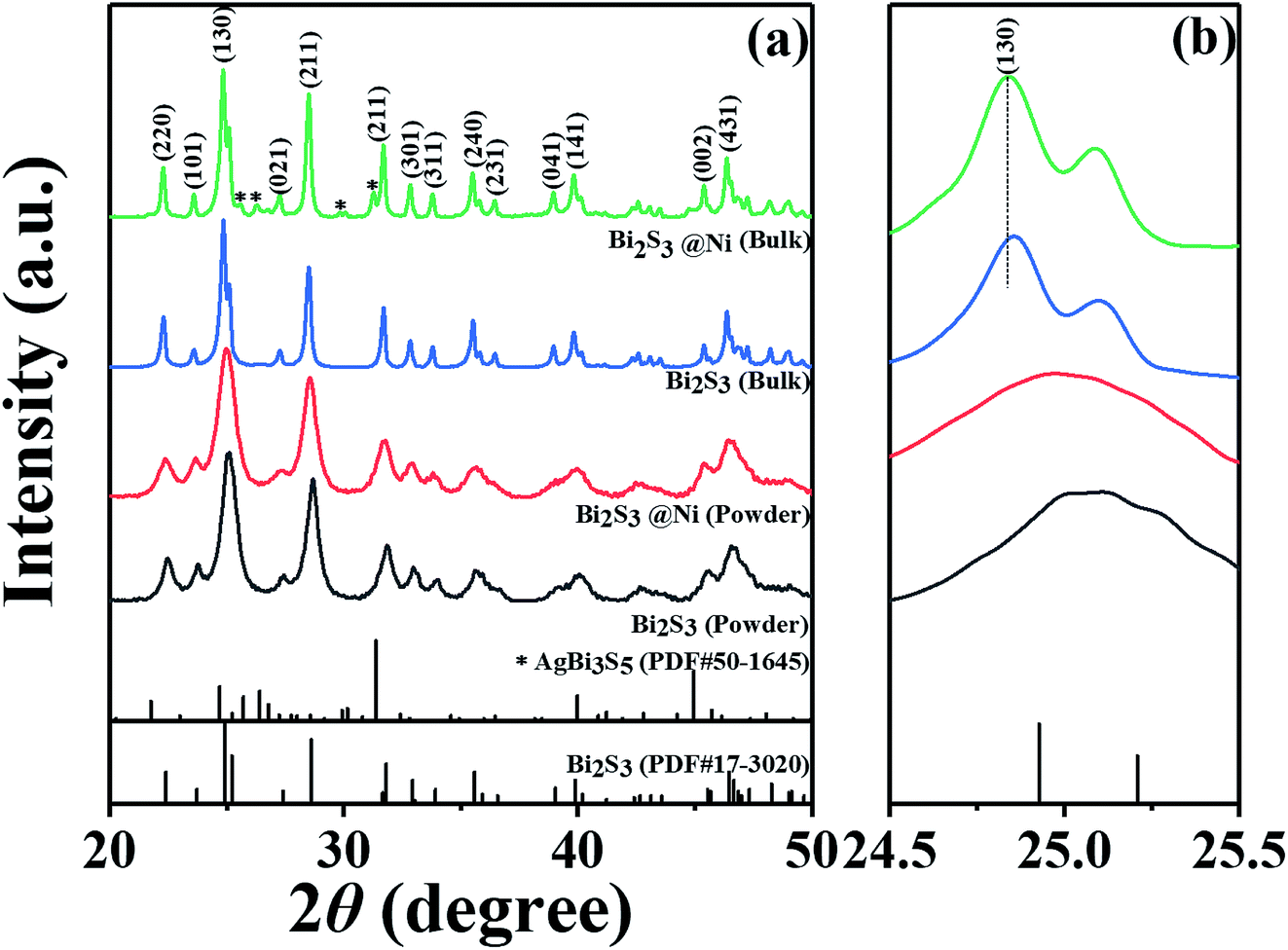 | ||
| Fig. 1 XRD patterns and the main peak enlargement patterns of Bi2S3 and BS@Ni powders and bulks. (a) XRD patterns of Bi2S3 and BS@Ni powders and bulks. (b) Main peak enlargement patterns of Bi2S3 and BS@Ni powders and bulks. | ||
The morphologies of Bi2S3 and BS@Ni powders are shown in Fig. 2(a) and (b). The morphologies of the powders before and after nickel plating are almost the same, which are consisted of different particles whose sizes ranging from 0.3 μm to 2 μm. Furthermore, Fig. 2(c) and (d) show the face element scanning results from the area of Fig. 2(a) and (b). As shown in the figures, the ratio of Bi content to S content in the pristine Bi2S3 powder is 39.60 to 60.40, which is close to the stoichiometry ratio of 2:3. On the other hand, the ratio of Bi to S of the BS@Ni powder is 38.68 to 58.79, which is the same as the ratio of pristine Bi2S3 powder. It indicates that the composition of Bi2S3 did not change during the nickel plating process. In addition, the content of Ag and Ni is only about 1.29% and 1.23% respectively. Combined with nickel plating process, we believe that due to the small size of micron-scale of powders, it is difficult to conduct coarsening or hydrophilic treatment, resulting in a difficult formation of Ag catalytic nucleation center in the activation process. Meanwhile, part of the catalytic nucleation center of Ag element failed to reduce Ni ions, so that the final powder contained only a small amount of Ni element and a small amount of residual Ag element. It is precisely because of the low contents of these two elements that the diffraction peaks cannot be observed in the XRD patterns.
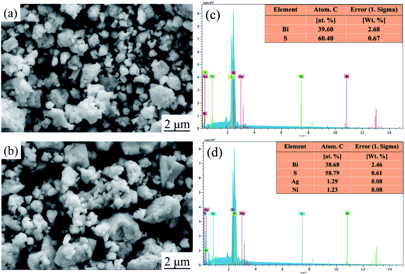 | ||
| Fig. 2 SEM images and face scanning results of element contents of Bi2S3 and BS@Ni powders. (a) SEM image of Bi2S3 powder, (b) SEM image of BS@Ni powder, (c) face element scanning result of Bi2S3 powder from (a), (d) face element scanning result of BS@Ni powder from (b). | ||
After sintering, the morphologies and mapping results of elements distribution of Bi2S3 and BS@Ni bulks are shown in Fig. 3. The morphology of Bi2S3 sintered block is relatively dense, which is consistent with the experimental result that the relative density of Bi2S3 bulk is 97.5%. In contrast, the relative density of BS@Ni is only 85%. As shown in Fig. 3(b), more pores in the BS@Ni bulk lead to its lower relative density. Combined with the XRD results of nickel plated block in Fig. 1(a), more pores in the morphology may be due to the fact that the silver particles which are on the surface of the powder reacted with the Bi2S3 substrate during the sintering process and generating AgBi3S5. It leads to the instability of the structure. The unstable structure leads to the loss of sulfur and generating more pores further. In addition, we also observe obvious layered structure in Fig. 3(b). What's more, the face scanning results of elements distribution are shown in the Fig. 3(c)–(f) respectively. As shown in Fig. 3(d), More Ni elements are distributed at the edge of Bi2S3 substrate but the distribution of Ag elements is relatively uniform, and there are partial distributions within the bulk in Fig. 3(f). The reason for this phenomenon may be that, in the recrystallization process of sintering, the theory of crystal growth kinetics shows that the Bi2S3 with layered structure is more likely to grow along the surface steps. The steps are also easy places to deposit Ni or Ag. Therefore, the Ni elements deposited on the surface of the substrate are continuously shifted to the boundary position as the crystal grows but the Ag elements reacted with the matrix and therefore obtaining a relatively uniform distribution. Finally, the result of element distribution is shown in Fig. 3(d) and (f). In order to facilitate the understanding, the process of nickel plating on bismuth sulfide powders and the element distribution in the sintered BS@Ni bulk are made into a schematic diagram, which is drawn in the Fig. 4.
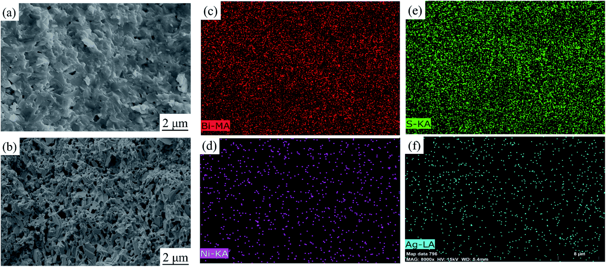 | ||
| Fig. 3 SEM images and face scanning results of element distribution of Bi2S3 and BS@Ni bulks. (a) SEM image of Bi2S3 bulk, (b) SEM image of BS@Ni bulk, (c) the Bi element distribution result of BS@Ni bulk, (d) the Ni element distribution result of BS@Ni bulk, (e) the S element distribution result of BS@Ni bulk, (f) the Ag element distribution result of BS@Ni bulk. | ||
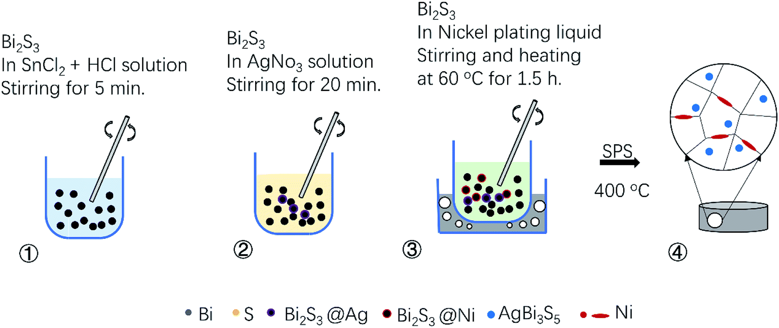 | ||
| Fig. 4 Schematic diagram of nickel plating process and element distribution of BS@Ni bulk. | ||
Further, the thermoelectric properties of Bi2S3 and Bi2S3@Ni bulks are shown in the Fig. 5. Among them, the errors of electrical properties are 3%, the errors of thermal properties are 5%, and the error of ZT value is 20%. Fig. 5(a) show the temperature-dependent electrical conductivities of Bi2S3 and BS@Ni bulks. The curves of electrical conductivity as a function of temperature exhibit distinct difference. The electrical conductivity of pristine Bi2S3 increases gradually with temperature rising, showing typical semiconductor behavior. At 628 K, the value of electrical conductivity of pristine Bi2S3 is only about 7.153 S cm−1. For the BS@Ni sample, the electrical conductivity monotonously decreases with the temperature increasing, showing typical strong degenerate semiconductor behavior. In numerical aspect, the value of electrical conductivity of BS@Ni sample decrease form 38.4 S cm−1 at 334 K to 28.9 S cm−1 at 628 K. The lowest value is four times that of the conductivity of the original Bi2S3 at the same temperature. This is because the second phase of AgBi3S5 with high conductivity (which is about 42 S cm−1) was produced during the preparation of nickel plated samples. The incorporation of the second phase and Ni elements resulted in the increase of S vacancies in the lattice and the enhancement of carrier concentration. At the same time, the Ni element distributing at the boundary position also improved the carrier mobility, so that the conductivity of the BS@Ni sample did not drop significantly with the increase of temperature as reported by Tan et al.,45 and the value remained four times that of the pristine bismuth sulfide.
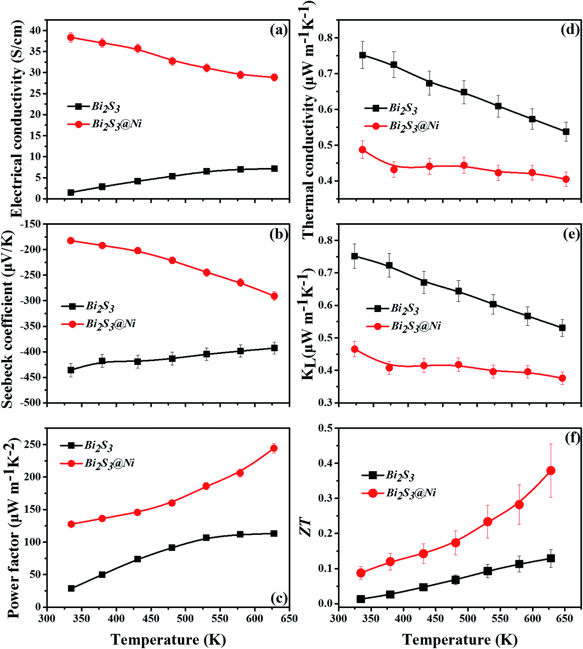 | ||
| Fig. 5 Thermoelectrical properties of Bi2S3 sample and BS@Ni sample. (a) Electrical conductivity, (b) Seebeck coefficient, (c) power factor, (d) thermal conductivity, (e) lattice thermal conductivity, (f) ZT. | ||
The temperature-dependent Seebeck coefficients of pristine Bi2S3 and BS@Ni sample are plotted in Fig. 5(b). All the samples show negative coefficient value in the whole measuring temperature range, indicating n-type semiconductors. For the pristine bismuth sulfide sample, the absolute value of Seebeck coefficient decreased with the increase of temperature. According to equation  , it is clear that the Seebeck coefficient is positively proportionate to the electron effective mass (m*) at Fermi level and negatively to the carrier concentration (n). Therefore, the absolute value of Seebeck coefficient of the pristine Bi2S3 sample decreases gradually with the increase of carrier concentration caused by intrinsic excitation with the temperature increasing. Also affected by the intrinsic excitation of BS@Ni sample, the absolute value of Seebeck coefficient of BS@Ni sample increases gradually with the temperature rising. For BS@Ni sample, the hole carriers induced by intrinsic excitation have a more obvious cancellation effect on most electron carriers, which makes the carrier concentration decrease with the increase of temperature, resulting in the increase of absolute value of Seebeck coefficient. Also limited by the high carrier mobility, the absolute value of Seebeck coefficient of BS@Ni sample did not reach the level of the pristine Bi2S3 sample, and the maximum value was 291 μV K−1 at 628 K.
Fig. 5(c) shows the temperature-dependent power factors of pristine Bi2S3 and BS@Ni samples, which are calculated from the formula PF = α|S|2, where α is electrical conductivity and S is Seebeck coefficient, respectively. As shown in the Fig. 5(c), PF of the BS@Ni samples is much higher than that of the pristine Bi2S3 sample at all temperature range due to the enhanced electrical transport properties by Ni plating. The peak value of 244 μW m−1 K−2 at 628 K for BS@Ni samples was two times higher than that of pristine Bi2S3 sample at the same temperature.
In usual, we will write the total thermal conductivity κtotal of solids as follows:
| κtotal = κlat + κel, | (1) |
| κel = LσT, | (2) |
 | (3) |
 | (4) |
Variations of the κtotal and κlat of Bi2S3 sample and BS@Ni sample with temperature are shown in Fig. 5(d) and (e). As shown in Fig. 5(d), the κtotal of BS@Ni sample is obviously lower than that of the pristine Bi2S3 sample. With the increase of temperature, the κtotal of BS@Ni samples gradually decreased from 0.48 W m−1 K−1 at room temperature to 0.40 W m−1 K−1 at 628 K, this was significantly lower than the 0.54 W m−1 K−1 of the pristine Bi2S3 sample at 628 K. This indicates that nickel plating is an effective method to reduce the κtotal of Bi2S3 materials. By comparing the values of κtotal and κlat in Fig. 5(d) and (e), it is not difficult to find that the κlat is dominant in the κtotal composition of the two samples. Compared with the pristine Bi2S3 sample, the κlat of BS@Ni sample decreased obviously. This indicates that the introduction of the second phase and the Ni element by the nickel plating process increased the scattering of phonons, resulting in the reduction of the κlat of the BS@Ni sample, and then led to a significant decrease in the κtotal of the BS@Ni sample.
The curves of ZT value of pristine Bi2S3 sample and BS@Ni sample are plotted in the Fig. 5(f). The ZT value of the BS@Ni sample is significantly higher than that of the pristine Bi2S3 sample due to the increased conductivity and decreased conductivity by nickel plating process. Its ZT value reaches the maximum value of 0.38 at 628 K, which is three times higher than that of pristine Bi2S3 materials. This proves that nickel plating is an effective method to optimize the thermoelectric properties of Bi2S3 materials.
Conclusion
In this work, BS@Ni samples was synthesized by electroless nickel plating on the mechanical alloying precursor-Bi2S3 powder and further spark plasma sintering. Its composition, microstructure, electrical and thermal transport properties have been investigated. Due to the influence of matrix particle size, the content of coating Ni elements are less, and there are a small amount of residual Ag elements. In the sintering process, residual Ag elements reacted with the base Bi2S3 material and formed AgBi3S5 second phase. The nickel element and AgBi3S5 second phase which introduced in the nickel plating process led to the increase of carrier concentration and mobility, resulting in significantly improvement of the electrical conductivity of BS@Ni sample. Meanwhile the Seebeck coefficient of BS@Ni sample still remained relatively high values of over 180 μV K−1 in the whole measuring temperature range. Therefore, the BS@Ni sample obtained a relatively high power factor of 244 μW m−1 K−2 at 628 K. Combined with a low thermal conductivity value of 0.40 W m−1 K−1 at 628 K, a maximum ZT value of 0.38 was obtained, which is three times higher than that of pristine Bi2S3 materials (ZT = 0.12). Therefore, nickel plating is an effective method to optimize the thermoelectric properties of Bi2S3 materials.Conflicts of interest
There are no conflicts to declare.Acknowledgements
This work was supported by the National Natural Science Foundation of China (Grant No. 11764025).References
- CRC Handbook of Thermoelectrics, ed. D. M. Rowe, 1995 Search PubMed.
- J. Yang and T. Caillat, MRS Bull., 2006, 31, 224 CrossRef CAS.
- G. J. Snyder and E. S. Toberer, Nat. Mater., 2008, 7, 105 CrossRef CAS PubMed.
- M. Zebarjadi, K. Esfarjani, M. S. Dresselhaus, Z. F. Ren and G. Chen, Energy Environ. Sci., 2012, 5, 5147 RSC.
- J. R. Sootsman, D. Y. Chung and M. G. Kanatzidis, Angew. Chem., Int. Ed., 2009, 48, 8616 CrossRef CAS PubMed.
- Y. Z. Pei, H. Wang and G. J. Snyder, Adv. Mater., 2012, 24, 6125 CrossRef CAS PubMed.
- J. P. Heremans, V. Jovovic, E. S. Toberer, A. Saramat, K. Kurosaki, A. Charoenphakdee, S. Yamanaka and G. J. Snyder, Science, 2008, 321, 554 CrossRef CAS PubMed.
- Y. Z. Pei, X. Y. Shi, A. Lalonde, H. Wang, L. D. Chen and G. J. Snyder, Nature, 2011, 473, 66 CrossRef CAS PubMed.
- W. S. Liu, X. Yan, G. Chen and Z. F. Ren, Nano Energy, 2012, 1, 42 CrossRef CAS.
- B. Poudel, Q. Hao, Y. Ma, Y. C. Lan, A. Minnich, B. Yu, X. A. Yan, D. Z. Wang, A. Muto, D. Vashaee, X. Y. Chen, J. M. Liu, M. S. Dersselhaus, G. Chen and Z. F. Ren, Science, 2008, 320, 634 CrossRef CAS PubMed.
- L. D. Zhao, V. P. Dravid and M. G. Kanatzidis, Energy Environ. Sci., 2014, 7, 251 RSC.
- K. Biswas, J. Q. He, I. D. Blum, C. I. Wu, T. P. Hogan, D. N. Seidman, V. P. Dravid and M. G. Kanatzidis, Nature, 2012, 489, 414 CrossRef CAS PubMed.
- L. D. Zhao, S. H. Lo, Y. Zhang, H. Sun, G. Tan, C. Uher, C. Wolveton, V. P. Dravid and M. G. Kanatzidis, Nature, 2014, 508, 373 CrossRef CAS PubMed.
- L. D. Zhao, D. Berardan, Y. L. Pei, C. Byl, L. Pinsard-Gaudart and N. Dragoe, Appl. Phys. Lett., 2010, 97, 092118 CrossRef.
- M. D. Nielsen, V. Ozolins and J. P. Heremans, Energy Environ. Sci., 2013, 6, 570 RSC.
- X. Yan, B. Poudel, Y. Ma, W. S. Liu, G. joshi, H. Wang, Y. C. Lan, D. Z. Wang, G. Chen and Z. F. Ren, Nano Lett., 2010, 10, 3373 CrossRef CAS PubMed.
- W. S. Liu, Q. Y. Zhang, Y. C. Lan, S. Shuo, X. Yan, Q. Zhang, H. Wang, D. Z. Wang, G. Chen and Z. F. Ren, Adv. Energy Mater., 2011, 1, 577 CrossRef CAS.
- W. S. Liu, K. C. Lukas, K. McEnaney, S. Lee, Q. Zhang, C. P. Opeil, G. Chen and Z. F. Ren, Energy Environ. Sci., 2013, 6, 552–560 RSC.
- L. D. Zhao, S. Q. Hao, S. H. Lo, C. I. Wu, X. Y. Zhou, Y. Lee, H. Li, K. Biswas, T. P. Hogan, C. Uher, C. Wolverton, V. P. Dravid and M. G. Kanatzidis, J. Am. Chem. Soc., 2013, 135, 7364 CrossRef CAS PubMed.
- L. D. Zhao, S. H. Lo, J. Q. He, H. Li, K. Biswas, J. Androulakis, C. I. Wu, T. P. Hogan, D. Y. Chung, V. P. Dravid and M. G. Kanatzidis, J. Am. Chem. Soc., 2011, 133, 20476 CrossRef CAS PubMed.
- X. Shi, J. Yang, J. R. Salvador, M. Chi, J. Y. Cho, H. Wang, S. Bai, J. Yang, W. Zhang and L. D. Chen, J. Am. Chem. Soc., 2011, 133, 7837 CrossRef CAS PubMed.
- S. Chen and Z. F. Ren, Mater. Today, 2013, 16, 387 CrossRef CAS.
- G. Joshi, T. Dahal, S. Chen, H. Z. Wang, J. Shiomi, G. Chen and Z. F. Ren, Nano Energy, 2013, 2, 82 CrossRef CAS.
- G. Joshi, H. Lee, Y. C. Lan, X. W. Wang, G. H. Zhu, D. Z. Wang, R. W. Gould, D. C. Cuff, M. Y. Tang, M. S. Dresselhaus, G. Chen and Z. F. Ren, Nano Lett., 2008, 8, 4670 CrossRef CAS PubMed.
- W. Liu, X. J. Tan, K. Yin, H. J. Liu, X. F. Tang, J. Shi, Q. J. Zhang and C. Uher, Phys. Rev. Lett., 2012, 108, 166601 CrossRef PubMed.
- J. Li, J. H. Sui, Y. L. Pei, C. Barreteau, D. Berardan, N. Dragoe, J. Q. He and L. D. Zhao, Energy Environ. Sci., 2012, 5, 8543 RSC.
- Y. He, T. Day, T. S. Zhang, H. L. Liu, X. Shi, L. D. Chen and G. J. Snyder, Adv. Mater., 2014, 26, 3974 CrossRef CAS PubMed.
- C. Chang, Y. Xiao, X. Zhang, Y. L. Pei, F. Li, S. L. Ma, B. F. Yuan, Y. Liu, S. K. Gong and L. D. Zhao, J. Alloys Compd., 2016, 664, 411–416 CrossRef CAS.
- S. Johnsen, J. Q. He, J. Androulakis, V. P. Dravid, L. Todorov, D. Y. Chung and M. G. Kanatzidis, J. Am. Chem. Soc., 2011, 133, 3460–3470 CrossRef CAS PubMed.
- W. Yao, D. F. Yang, Y. C. Yan, K. L. Peng, H. Zhang, A. P. Liu, X. Lu, G. Y. Wang and X. Y. Zhou, ACS Appl. Mater. Interfaces, 2017, 9, 10595–10601 CrossRef CAS PubMed.
- Y. He, T. Day, T. S. Zhang, H. L. Liu, X. Shi, L. D. Chen and G. J. Snyder, Adv. Mater., 2014, 26, 3974–3978 CrossRef CAS PubMed.
- Q. Tan, L. D. Zhao, J. F. Li, C. F. Wu, T. R. Wei, Z. B. Xing and M. G. Kanatzidis, J. Mater. Chem. A, 2014, 2, 17302 RSC.
- J. H. Li, Q. Tan and J. F. Li, J. Alloys Compd., 2013, 551, 143–149 CrossRef CAS.
- B. X. Chen and C. Uher, Chem. Mater., 1997, 9, 1655–1658 CrossRef CAS.
- L. D. Zhao, B. P. Zhang, W. S. Liu, H. L. Zhang and J. F. Li, J. Solid State Chem., 2008, 181, 3278–3282 CrossRef CAS.
- A. A. Rahman, R. Huang and L. Whittaker-Brooks, Chem. Mater., 2016, 28, 6544–6552 CrossRef CAS.
- L. Li, Y. Liu, J. Y. Dai, H. X. Zhu, A. J. Hong, X. H. Zhou, Z. F. Ren and J. M. Liu, Nano Energy, 2015, 12, 447–456 CrossRef CAS.
- Z. H. Ge, B. P. Zhang, Y. Q. Yu and P. P. Shang, J. Alloys Compd., 2002, 514, 205–209 CrossRef.
- Y. Q. Yu, B. P. Zhang, Z. H. Ge, P. P. Shang and Y. X. Chen, Mater. Chem. Phys., 2011, 131, 216–222 CrossRef CAS.
- Z. H. Ge, B. P. Zhang, Y. Liu and J. F. Li, Phys. Chem. Chem. Phys., 2012, 14, 4475–4481 RSC.
- V. Tarachand, R. Sharma, V. Bhatt and G. S. Ganesan, Nano Res., 2016, 9, 3291–3304 CrossRef.
- Y. Kawamoto and H. Iwasaki, J. Electron. Mater., 2014, 43, 1475–1479 CrossRef CAS.
- F. Han, H. Liu, C. D. Malliakas, M. Sturza, D. Y. Chung, X. Wan and M. G. Kanatzidis, Inorg. Chem., 2016, 55, 3547–3552 CrossRef CAS PubMed.
- L. J. Zhang, B. P. Zhang, Z. H. Ge and C. G. Han, Solid State Commun., 2013, 162, 48–52 CrossRef CAS.
- G. Tan, S. Hao, J. Zhao, C. Wolverton and M. G. Kanatzidis, J. Am. Chem. Soc., 2017, 139, 6467–6473 CrossRef CAS PubMed.
| This journal is © The Royal Society of Chemistry 2019 |