DOI:
10.1039/C9RA04655K
(Paper)
RSC Adv., 2019,
9, 23142-23147
Modulation of the electronic property of hydrogenated 2D tetragonal Ge by applying external strain
Received
21st June 2019
, Accepted 22nd July 2019
First published on 26th July 2019
Abstract
Inspired by the novel properties of a newly predicted two-dimensional (2D) tetragonal allotrope of Ge called 2D tetragonal Ge, first-principles calculations have been performed to explore the stability, and structural and electronic properties of 2D tetragonal Ge via hydrogenation, and the effect of external strain on structural and electronic properties of hydrogenated 2D tetragonal Ge is considered. Our calculations reveal that the hydrogenated 2D tetragonal Ge, α-GeH and β-GeH, are proved to be dynamically and thermally stable. Both α-GeH and β-GeH are semiconductors with a direct band gap of 0.953 eV and indirect band gap of 2.616 eV, respectively. When applying external strain from −7% to 7%, α-GeH is more energetically stable than β-GeH around the equilibrium geometry, β-GeH is more stable than α-GeH when external strains exceed a certain critical value, respectively. The direct band gap of α-GeH reduces rapidly from 2.008 eV to 0.036 eV as external strain increases from −7% to 7%, while the indirect band gap of β-GeH is changed slightly. Our results reveal that α-GeH and β-GeH can offer an intriguing platform for nanoscale device applications and spintronics.
1. Introduction
Following the successful preparation of graphene,1 two-dimensional (2D) materials, including silicene,2 germanene,3 hexagonal boron nitride,4 transition metal dichalcogenides (TMDs),5 and phosphorene,6 have attracted extensive attention due to their outstanding electronic, optical, thermal and mechanical properties. In analogy to graphene, it is theoretically predicted that other group IV elements can form stable 2D honeycomb structures, namely silicene and germanene, and they have been successfully synthesized on different substrates.2,3 More recently, a 2D tetragonal allotrope of C consisting of repeated square and octagonal rings was predicted to be stable.7 First-principles calculations have proposed that the 2D tetragonal allotrope of Si is a nodal line semimetal, and hydrogenation could induce a semimetal–semiconductor transition in this silicene allotrope.8 Also, 2D tetragonal Ge and tetragonal Sn are theoretically predicted to be nodal line semimetals which are identified by nontrivial Z2 invariant and topological edge states at the sample boundaries.9 Additionally, some tetragonal graphene-like analogues, such group V elements, XBi (X = Si, Ge, Sn) and TMDs, have also been proposed and predicted to be stable.10–16
It is crucial to open the band gap of 2D group IV materials for broadening the application in semiconductor devices, such as in power components and optoelectronic fields. Hydrogenation has been demonstrated to be one of the most accessible ways to modulate the properties of 2D materials. In this respect, it has been theoretically reported that hydrogenation significantly modifies the band properties and band gap of graphene, silicene and germanene,17 deriving them from semimetal state to a semiconductor state with a large band gap, and which have been synthesized in experiments.18–20 The band gap of 8-Pmmn borophene has been opened by hydrogenation.21 The hydrogenation causes monolayer GaN to undergo an indirect to direct band gap transition.22 Generally speaking, external strain engineering is the other effective approach in modifying the electronic band structure of low dimensional materials. It is found that 2D materials, such as graphene, phosphorene and MoS2, can withstand a tensile strain of more than 20%.23–25 PbTe films passivated with H atoms are semiconductors with a direct band gap of 0.015 eV, and the direct band gap can be tuned from 0.015 eV to 0.065 eV under external strain.26 The tensile strain can tune the band gap of GaN monolayer in the broad range of 4.44–2.27 eV.22 The 2D tetragonal XBi (X = Si, Ge, Sn) undergo a transition from a direct to indirect band gap or an indirect band gap semiconductor to metal by applying biaxial strain.16 It has been reported that the electronic property of monolayer CrI3 can be modified by applying strain, which undergoes a transition from magnetic-metal to half-metal to half-semiconductor to spin-relevant semiconductor as strain increases from −15% to 10%.27 The band gap of phosphorene experiences a direct–indirect–direct transition when axial strain is applied.23 It is indicated that compressive strain induces 1T-HfS2 monolayer to undergo a semiconductor–metal transition.28
In the paper, we systematically investigate the stability, geometry structure and electronic property of 2D tetragonal Ge via hydrogenation, where two different atomic configurations are considered. We also explore the effect of external strain on the structural and electronic properties in the hydrogenated 2D tetragonal Ge.
2. Computational details
Our calculations were carried out based on the density functional theory in the Vienna ab initio Simulation Package (VASP)29–31 within the projector-augmented wave (PAW) method.32 The Perdew–Burke–Ernzerhof (PBE) of the generalized gradient approximation (GGA)33 was used as exchange–correlation functional. The kinetic energy cutoff of the plane wave basis was set at 500 eV. The vacuum space more than 20 Å was placed to avoid the interaction between the neighboring slabs. All structures were fully relaxed until the energy tolerances were smaller than 1 × 10⁻⁶ eV and the force on each atom was less than 0.01 eV Å−1. The Brillouin zone was performed of a 13 × 13 × 1 k-points. The HSE06 calculation was also used to check the validity of electronic band structure given by the PBE calculation. The spin-orbital-coupling (SOC) effect was considered in the calculation of the band structure. To examine the dynamic stability of the hydrogenated 2D tetragonal Ge, the phonon dispersions were performed by the finite displacement method in the PHONOPY code.34 The ab initio molecular dynamics (AIMD) simulations were implemented to check the thermally stability at 300 K in the canonical (NVT), where the simulation time is limited to 10 ps with a time step of 1 fs. The binding energy was calculated to check the energetic stability, and the binding energy was defined by Eb = (EGeH − nEGe − nEH)/2n,18 where EGeH is the total energy of the hydrogenated 2D tetragonal Ge, EGe and EH are the energies of the isolated Ge and H atoms, respectively, and n is the number of Ge or H atom in the unit.
The applied external strain was defined as η = (a − a0)/a0, where a0 is the lattice constant of the optimized strain-free structure, a is the lattice constant of the strained systems, and just atomic position was allowed to relax for strained system. Negative and positive values of η referred to compressive strain and tensile strain, respectively. The external strains in the range of −7% to 7% with spacing of 1% were chosen in our calculations. In this work, two types of external strains, biaxial strain and uniaxial strain along the x direction, were applied on α-GeH and β-GeH.
3. Results and discussion
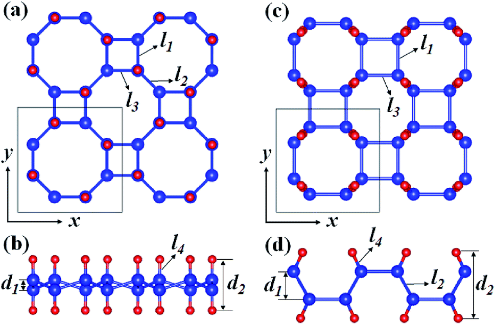
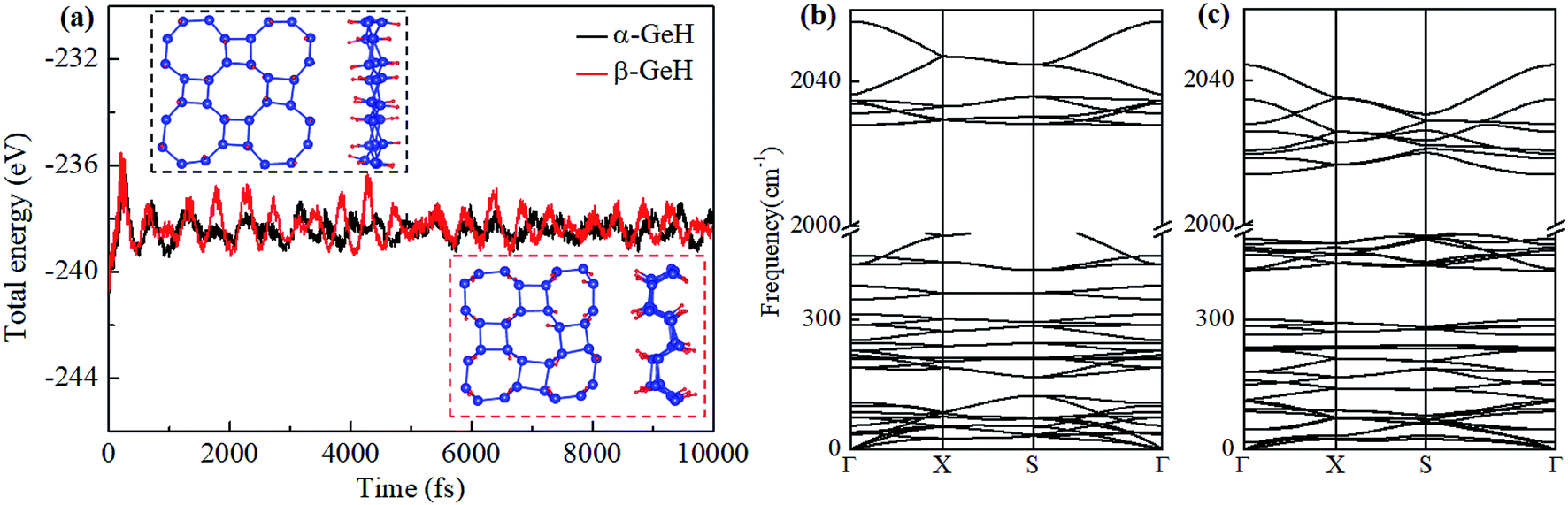
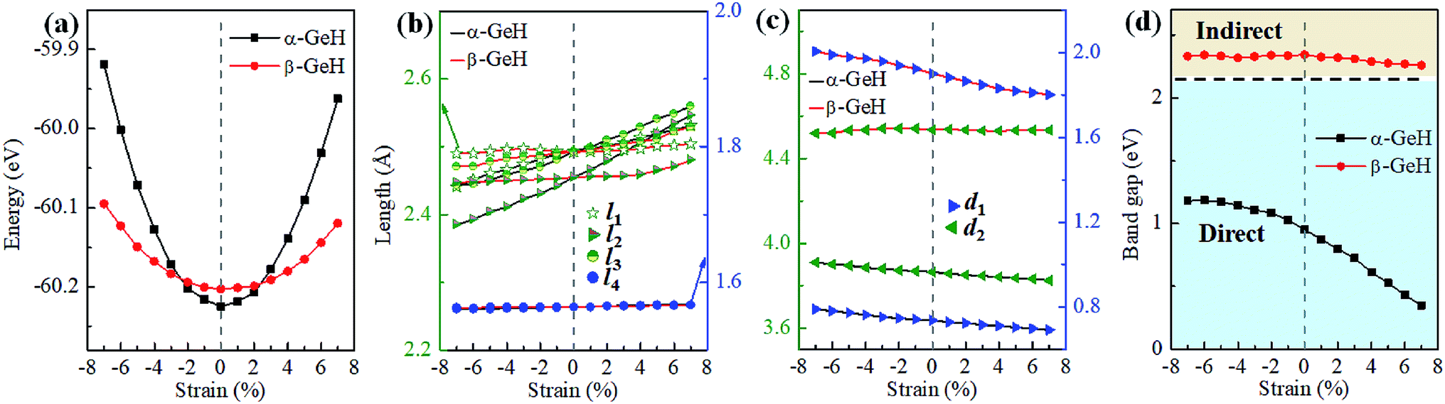
Fig. 1 depicts the optimized atomic structures of two hydrogenated 2D tetragonal Ge, denoted by α-GeH with the hydrogen atoms alternate on both sides of the sheet and β-GeH with the hydrogen atoms alternate in pairs of the sheet. The optimized structural parameters of α-GeH and β-GeH, including lattice constants a0, Ge–Ge bond lengths l1 and l2, and the vertical distance between top and bottom Ge(H) layers d1 (d2), are summarized in Table 1. Except for the lattice constant of β-GeH, all the corresponding parameters of α-GeH and β-GeH are enlarged in comparison to pristine 2D tetragonal Ge. As listed in Table 1. The calculated binding energies are −2.832 eV per atom and β-GeH −2.832 eV per atom of α-GeH and β-GeH, respectively, indicating strong interactions between H atom and Ge atom. According to previous calculations, the binding energy of hydrogenated germanene is −2.882 eV per atom,17 and hydrogenated germanene has been synthesized in experiment,18 it indicates that α-GeH and β-GeH are stable and possible to experimentally obtained. Additionally, AIMD simulations are carried out at 300 K for 10 ps, and the total energies with respect to the simulation time and the final structure after simulations are displayed in Fig. 2(a). The total energies are fluctuated within a narrow range during simulations for both α-GeH and β-GeH, and the original structures can be nearly kept after the simulations, confirming the thermally stable of α-GeH and β-GeH. Furthermore, the phonon dispersions of α-GeH and β-GeH are calculated and displayed in Fig. 2(b) and (c), there is no any imaginary frequency in the Brillouin zone, conforming the dynamic stability of α-GeH and β-GeH.
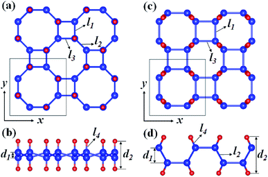 |
| | Fig. 1 Optimized geometries of (a) and (b) α-GeH and (c) and (d) β-GeH. The blue and red balls indicate Ge and H atoms, respectively. | |
Table 1 The lattice constant a0, Ge–Ge bond lengths l1 and l2 (l3), Ge–H bond length l4, and the vertical distance between top and bottom Ge(H) layers d1 (d2) shown in Fig. 1, band gap Eg, and binding energy Eb of α-GeH and β-GeH
| System |
a0 (Å) |
l1 (Å) |
l2 (l3) (Å) |
l4 (Å) |
d1 (Å) |
d2 (Å) |
Eg (eV) |
Eb (eV per atom) |
| Ge9 |
8.007 |
2.481 |
2.412 |
— |
0.717 |
— |
0.000 |
−3.082 |
| α-GeH |
8.073 |
2.493 |
2.455 |
1.564 |
0.737 |
3.865 |
0.953 |
−2.832 |
| β-GeH |
7.184 |
2.492 |
2.455 |
1.564 |
1.870 |
4.535 |
2.343 |
−2.830 |
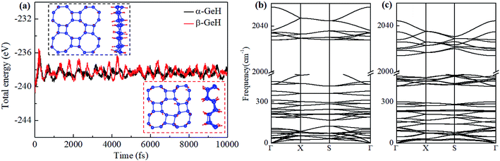 |
| | Fig. 2 (a) The total energy fluctuation of α-GeH (black line) and β-GeH (red line), the insets are the final structures at the end of AIMD simulations. Phonon dispersions for (b) α-GeH and (c) β-GeH. | |
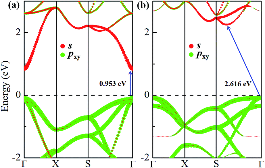
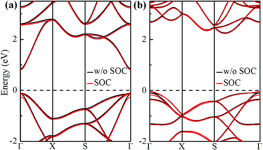
The electronic band structures of α-GeH and β-GeH are calculated and plotted in Fig. 3. An energy gap opens in 2D tetragonal Ge by hydrogenation, α-GeH and β-GeH are both semiconductors, the type of gap for hydrogenated 2D tetragonal Ge depends on its atomic configuration. It can be clearly seen from Fig. 3, α-GeH is direct band gap of 0.953 eV with the valence band maximum (VBM) and conduction band minimum (CBM) at the Γ point, while β-GeH is indirect band gap of 2.616 eV with its VBM lying at Γ point and CBM locating along the S–Y direction. As shown in Fig. 3, the VBM and CBM of α-GeH and β-GeH are originated from the pxy and s orbitals of Ge atom, respectively. In order to examine the effect of SOC, the electronic band structures of α-GeH and β-GeH with considering the SOC effect are calculated and displayed in Fig. 4. It can be seen from Fig. 4 that taking into account SOC, the band gaps of the unstrained α-GeH and β-GeH is reduced slightly, which are changed to 0.904 eV and 2.275 eV. Compared to band structures without SOC, there is no remarkable change in band gap and the shapes of the electronic structure near the Fermi level are essentially unchanged. Therefore, the effect of SOC on the electronic structure for α-GeH and β-GeH are negligible. Then, the HSE calculation is used to check the electronic band structure of α-GeH and β-GeH, and the results are displayed in Fig. 5. It is clear that overall electronic band profiles calculated by PBE and HSE calculations are similar, the only difference is the calculated band gap, the HSE calculation enhance the band gap to 1.414 eV and 3.036 eV for α-GeH and β-GeH, respectively. Our work is mainly focused on the external strain effect on the band structure of α-GeH and β-GeH, and the HSE calculation could give results of the strain effects on the band structures consistent with that of the PBE calculation. The PBE calculation can able to correctly predict the trends of external strain effect on the electronic band structure and band gap for α-GeH and β-GeH.
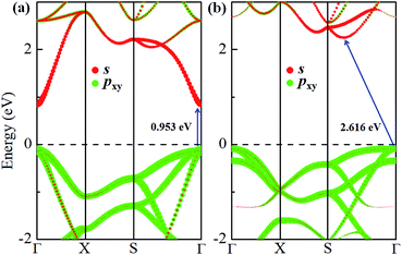 |
| | Fig. 3 Orbital-resolved band structures of unstrained (a) α-GeH and (b) β-GeH, red and green dots represent the contribution from Ge-pxy and Ge-s, respectively. The Fermi levels are set to zero. | |
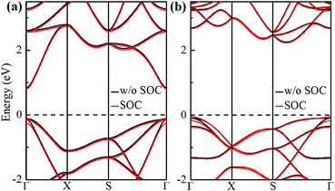 |
| | Fig. 4 Band structures of (a) α-GeH and (b) β-GeH without SOC (black lines) and with SOC (red lines). The Fermi level is set at zero. | |
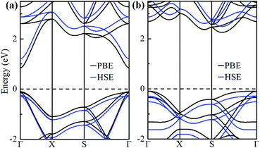 |
| | Fig. 5 Band structures of (a) α-GeH and (b) β-GeH by using PBE (black lines) and HSE (blue lines) calculations. The Fermi level is set at zero. | |
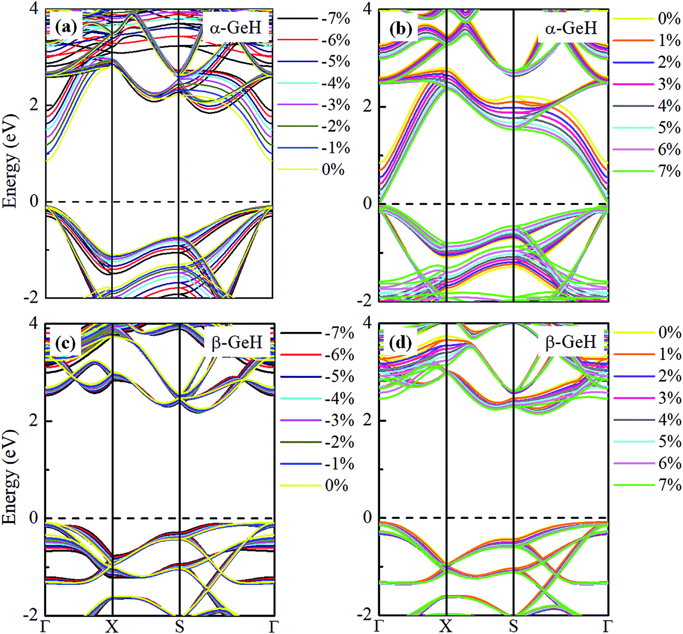
Recently, both experimental and theoretical studies have investigated that the electronic structure can be modulated by applying external strain. Here, we discuss the effect of external strain on the geometry structure and electronic band structures of α-GeH and β-GeH, and the applied external strains ranged from −7% to 7%. First, we study the case of applying biaxial strain, the total energies with respect to biaxial strain for α-GeH and β-GeH are calculated and the results can be seen from Fig. 6(a) α-GeH is more energetically stable than β-GeH under strains in the range ±2%, while β-GeH is more stable than α-GeH when strains larger than ±2%. Furthermore, the detailed analysis of the geometric structure for strained α-GeH and β-GeH are also carried out. In Fig. 6(b), it can be clearly seen that the bond lengths l1 and l2 enhance linearly for α-GeH under biaxial strains from −7% to 7%, while those of β-GeH display a very slightly increase, the bond length l3 is hardly affected by biaxial strain and maintains a constant about 1.564 Å for both α-GeH and β-GeH. When applying biaxial strains from −7% to 7%, the interlayer distance d1 of α- and β-GeH and d2 of α-GeH decrease monotonously, the interlayer distance d2 of β-GeH changes little as biaxial strain increases in Fig. 6(c).
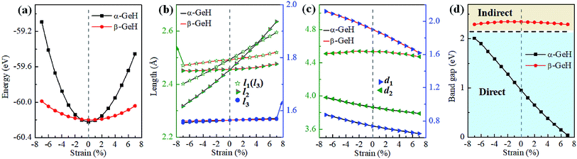 |
| | Fig. 6 The variations of (a) energies, (b) bond lengths, (c) vertical distances, and (d) band gaps of α-GeH and β-GeH as a function of biaxial strains. The direct and indirect band gap regions are highlighted with blue and orange, respectively. | |
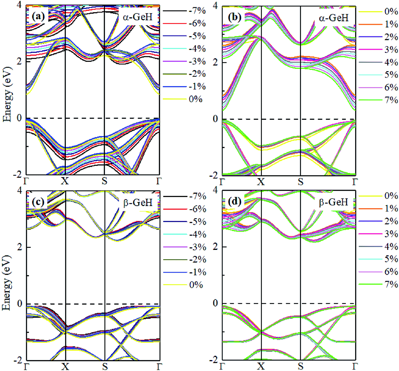
Hence, the electronic band structure of α-GeH and β-GeH under biaxial strains between −7% and 7% are investigated, the results are displayed in Fig. 7. As can be seen from Fig. 7(a) and (b), α-GeH is always remaining direct band gap character, the CBM at the Γ point of α-GeH shifts downward in a linear way and the VBM at the Γ point shifts upward very slowly under biaxial strains of −7% to 7%. As displayed in Fig. 7(c) and (d), β-GeH keeps indirect band gap property, the location of the VBM and CBM is almost unaffected within the biaxial strains range of −7% to 7%. It can been seen in Fig. 6(d), the direct band gap of α-GeH decreases sharply as the strain increases in the range from −7% to 7%, which change from 2.008 eV to 0.036 eV, while the band gap of β-GeH changes slightly. The variation of band gap for α-GeH and β-GeH also reflects the changes in their structure. In Fig. 6(b), the distance between the upper Ge atom and the lower Ge atom (bond lengths l1 and l2) increases linearly as strain increases, causing the bond between them to become weaker and weaker, therefore, the band gap of α-GeH is gradually reduced. For β-GeH, the bond lengths l1 and l2 varies slowly under biaxial strain, leading to little change in the band gap of β-GeH. Then, the uniaxial strain effects on geometric and electronic properties of α-GeH and β-GeH are also studied, and the calculation results are shown in Fig. 8 and 9. As mentioned above, the tendency in energies, bond lengths, vertical distances and band gaps of α-GeH and β-GeH is similar to that of applying biaxial strain. It can be seen from Fig. 8(a), α-GeH is more energetically stable than β-GeH under strains in the range ±3%, while β-GeH is more stable than α-GeH with strains larger than ±3%. When applying uniaxial strains from −7% to 7%, the band gap of α-GeH can be tuned from 1.181 eV to 0.349 eV, as plotted in Fig. 8(d). Our calculations show that α-GeH and β-GeH remain their direct or indirect behavior under the biaxial and uniaxial strains and the band gap of α-GeH can be tuned in a wide range.
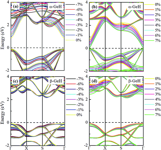 |
| | Fig. 7 Electronic band structures of (a) and (b) α-GeH, and (c) and (d) β-GeH under different biaxial strains. The Fermi levels are set to zero. | |
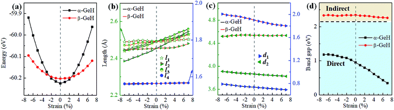 |
| | Fig. 8 The variations of (a) energies, (b) bond lengths, (c) vertical distances, and (d) band gaps of α-GeH and β-GeH as a function of uniaxial strains. The direct and indirect band gap regions are highlighted with blue and orange, respectively. | |
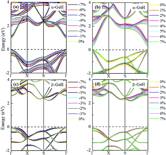 |
| | Fig. 9 Electronic band structures of (a) and (b) α-GeH, and (c) and (d) β-GeH under different uniaxial strains. The Fermi levels are set to zero. | |
4. Conclusions
In summary, based on first-principles calculations, we systemically study the stability, structural and electronic properties of 2D tetragonal Ge by hydrogenation, and the influence of external strain on the structural and electronic properties of the hydrogenated 2D tetragonal Ge is also investigated. Our calculated results indicate that α-GeH is a direct semiconductor with a band gap of 0.953 eV, while β-GeH is an indirect semiconductor with a band gap of 2.616 eV. Applying external strains from −7% to 7%, α-GeH is more energetically stable than β-GeH around the equilibrium geometry, β-GeH is more stable than α-GeH when external strains exceed a certain critical value, respectively. The band gap of α-GeH can be effectively tuned by applying external strain, which changes from 2.008 eV to 0.036 eV when the applied external strain varies from −7% to 7%, while the band gap of β-GeH is insensitive to external strain. α-GeH and β-GeH possess excellent electronic property, showing great potential in nano-electric devices and spintronics.
Conflicts of interest
There are no conflicts to declare.
Acknowledgements
This work was supported by the Specialized Fund for the Doctoral Research of Jilin Engineering Normal University under Grants No. BSKJ201904, the China Postdoctoral Science Foundation (2019M652560), the postdoctoral research grant in Henan Province (1902013) and the Startup Research Fund of Zhengzhou University (32211173).
References
- A. K. Geim and K. S. Novoselov, Nat. Mater., 2007, 6, 183 CrossRef CAS PubMed.
- B. Feng, Z. Ding, S. Meng, Y. Yao, X. He, P. Cheng, L. Chen and K. Wu, Nano Lett., 2012, 12, 3507–3511 CrossRef CAS PubMed.
- M. E. Dávila, L. Xian, S. Cahangirov, A. Rubio and G. Le Lay, New J. Phys., 2014, 16, 095002 CrossRef.
- L. Song, L. Ci, H. Lu, P. B. Sorokin, C. Jin, J. Ni, A. G. Kvashnin, D. G. Kvashnin, J. Lou, B. I. Yakobson and P. M. Ajayan, Nano Lett., 2010, 10, 3209–3215 CrossRef CAS PubMed.
- Q. H. Wang, K. Kalantar-Zadeh, A. Kis, J. N. Coleman and M. S. Strano, Nat. Nanotechnol., 2012, 7, 699 CrossRef CAS PubMed.
- L. Li, Y. Yu, G. J. Ye, Q. Ge, X. Ou, H. Wu, D. Feng, X. H. Chen and Y. Zhang, Nat. Nanotechnol., 2014, 9, 372 CrossRef CAS PubMed.
- Y. Liu, G. Wang, Q. Huang, L. Guo and X. Chen, Phys. Rev. Lett., 2012, 108, 225505 CrossRef.
- H. Wu, Y. Qian, Z. Du, R. Zhu, E. Kan and K. Deng, Phys. Lett. A, 2017, 381, 3754–3759 CrossRef CAS.
- C. Xu, Y. Wang, R. Han, H. Tu and Y. Yan, New J. Phys., 2019, 21, 033005 CrossRef.
- Y. Zhang, J. Lee, W.-L. Wang and D.-X. Yao, Comput. Mater. Sci., 2015, 110, 109–114 CrossRef CAS.
- K. Liangzhi, T. Xin, M. Yandong, T. Hassan, Z. Liujiang, S. Ziqi, A. Du, C. Changfeng and C. S. Sean, 2D Mater., 2015, 2, 045010 CrossRef.
- F. Ersan, E. Aktürk and S. Ciraci, Phys. Rev. B: Condens. Matter Mater. Phys., 2016, 94, 245417 CrossRef.
- Y. Sun, C. Felser and B. Yan, Phys. Rev. B: Condens. Matter Mater. Phys., 2015, 92, 165421 CrossRef.
- S. M. Nie, Z. Song, H. Weng and Z. Fang, Phys. Rev. B: Condens. Matter Mater. Phys., 2015, 91, 235434 CrossRef.
- Y. Ma, L. Kou, X. Li, Y. Dai, S. C. Smith and T. Heine, Phys. Rev. B: Condens. Matter Mater. Phys., 2015, 92, 085427 CrossRef.
- C. Xu, M. Zhu, J. Zhang, W. Wang and Y. Yan, Comput. Mater. Sci., 2018, 150, 314–320 CrossRef CAS.
- J. Kang, J. Li, F. Wu, S.-S. Li and J.-B. Xia, J. Phys. Chem. C, 2011, 115, 20466–20470 CrossRef CAS.
- E. Bianco, S. Butler, S. Jiang, O. D. Restrepo, W. Windl and J. E. Goldberger, ACS Nano, 2013, 7, 4414–4421 CrossRef CAS PubMed.
- J. Qiu, H. Fu, Y. Xu, A. I. Oreshkin, T. Shao, H. Li, S. Meng, L. Chen and K. Wu, Phys. Rev. Lett., 2015, 114, 126101 CrossRef PubMed.
- D. C. Elias, R. R. Nair, T. M. G. Mohiuddin, S. V. Morozov, P. Blake, M. P. Halsall, A. C. Ferrari, D. W. Boukhvalov, M. I. Katsnelson, A. K. Geim and K. S. Novoselov, Science, 2009, 323, 610 CrossRef CAS PubMed.
- Z.-Q. Wang, T.-Y. Lü, H.-Q. Wang, Y. P. Feng and J.-C. Zheng, ACS Appl. Electron. Mater., 2019, 1, 667–674 CrossRef CAS.
- H. Shu, X. Niu, X. Ding and Y. Wang, Appl. Surf. Sci., 2019, 479, 475–481 CrossRef CAS.
- X. Peng, Q. Wei and A. Copple, Phys. Rev. B: Condens. Matter Mater. Phys., 2014, 90, 085402 CrossRef.
- A. Castellanos-Gomez, M. Poot, G. A. Steele, H. S. J. van der Zant, N. Agraït and G. Rubio-Bollinger, Nanoscale Res. Lett., 2012, 7, 233 CrossRef PubMed.
- K. S. Kim, Y. Zhao, H. Jang, S. Y. Lee, J. M. Kim, K. S. Kim, J.-H. Ahn, P. Kim, J.-Y. Choi and B. H. Hong, Nature, 2009, 457, 706 CrossRef CAS PubMed.
- Z. Huang and D. Zhang, J. Phys.: Condens. Matter, 2019, 31, 295503 CrossRef CAS PubMed.
- Z. Wu, J. Yu and S. Yuan, Phys. Chem. Chem. Phys., 2019, 21, 7750–7755 RSC.
- N. Wu, X. Zhao, X. Ma, Q. Xin, X. Liu, T. Wang and S. Wei, Phys. E, 2017, 93, 1–5 CrossRef CAS.
- G. Kresse and J. Hafner, Phys. Rev. B: Condens. Matter Mater. Phys., 1994, 49, 14251–14269 CrossRef CAS PubMed.
- G. Kresse and J. Hafner, Phys. Rev. B: Condens. Matter Mater. Phys., 1993, 47, 558–561 CrossRef CAS PubMed.
- G. Kresse and J. Furthmüller, Phys. Rev. B: Condens. Matter Mater. Phys., 1996, 54, 11169–11186 CrossRef CAS PubMed.
- P. E. Blöchl, Phys. Rev. B: Condens. Matter Mater. Phys., 1994, 50, 17953–17979 CrossRef PubMed.
- J. P. Perdew, K. Burke and M. Ernzerhof, Phys. Rev. Lett., 1996, 77, 3865–3868 CrossRef CAS PubMed.
- D. Alfè, Comput. Phys. Commun., 2009, 180, 2622–2633 CrossRef.
|
| This journal is © The Royal Society of Chemistry 2019 |
Click here to see how this site uses Cookies. View our privacy policy here. 
 Open Access Article
 This Open Access Article is licensed under a Creative Commons Attribution-Non Commercial 3.0 Unported Licence
 a,
Jing Zhanga,
Ming Guoa and
Lingrui Wang*b
a,
Jing Zhanga,
Ming Guoa and
Lingrui Wang*b