
 Open Access Article
 This Open Access Article is licensed under a Creative Commons Attribution-Non Commercial 3.0 Unported Licence
Comparative study of aqueous solution processed ZnO/GaAs and ZnO/porous GaAs films
E. Ben Amara a,
A. Lebib*a,
Z. Zaaboubb and
L. Bejiac
a,
A. Lebib*a,
Z. Zaaboubb and
L. Bejiac
aUniversité de Sousse, Ecole Supérieure des Sciences et de la Technologie, Laboratoire des Energies et des Matériaux, LabEM-LR11ES34, Rue Lamine Abassi, 4011 Hammam Sousse, Tunisia. E-mail: amiralebib@gmail.com
bLaboratoire de Micro-optoélectronique et Nanostructures, Faculté des sciences de Monastir, Bd environnement, 5019 Monastir, Tunisia
cPhysics Department, College of Science & Arts, Qassim University, Ar Rass, Al Qassim Province, Kingdom of Saudi Arabia
First published on 15th August 2019
Abstract
In this paper, we investigate the structural and photoluminescence properties of aqueous solution-processed ZnO/GaAs and ZnO/porous GaAs films. According to X-ray diffraction (XRD) analysis, a ZnO film deposited on porous GaAs shows a monocrystalline structure with a-axis orientation, which is desirable for light emitting applications. The results obtained from atomic force microscopy (AFM) data confirm that a porous GaAs substrate is beneficial to deposit a uniform array of ZnO nanostructures with sizes down to 12 nm and a relatively low surface roughness (2.6 nm). Under excitation wavelength λexc = 375 nm, ZnO/GaAs and ZnO/porous GaAs films showed emissions in most of the visible spectral region (450–750 nm). Our study reveals that changing the wavelength of the excitation UV radiation makes it possible to control the photoluminescence (PL) properties of ZnO films. Enhancement of the PL intensity was noticed in the UV and visible spectral regions when ZnO is deposited on porous GaAs, which is promising for optoelectronic device applications.
1. Introduction
Over the last decade, there has been a significantly growing interest in semiconducting metal oxide nanomaterials because of their noticeable optical and electric properties, but also for their technological applications in the future. In particular, ZnO has emerged as one of the most favorable candidates because it exhibits a wide band gap (3.3 eV) and a high binding energy of excitons (60 meV).1 Further, it can be developed into new nanostructures with various shapes, such as nanosprings and nanobelts.2Nanosized ZnO can be synthesized by different techniques such as hydrothermal,3 chemical vapour deposition (CVD),4 sputtering deposition,5 RF magnetron sputtering,6 and solution growth.7–9 Among those techniques, solution-based deposition processes attracted great interest mainly for the low cost production and the possibility of obtaining uniform films over a large-area. So far, attempts have been made to develop solution processed thin film transistors and ultraviolet photodetectors with competetive performances.7–10 For flexible electronic devices, Meyers et al. developed ammine hydroxo zinc complex as a new precursor for solution processed thin films applicable at low temperatures (T ≤ 300 °C).11
Thin films of ZnO developed on different substrates show different structural, optical and electrical properties. In particular, white light emission from ZnO/porous silicon nanocomposites was reported by many authors.12–15 Naddaf et al. reported room temperature photoluminescence properties of Al-doped ZnO film grown on porous GaAs by radio frequency magnetron sputtering technique. The authors demonstrate the contribution of porous GaAs to the enhancement of photoluminescence intensity of the ZnO film in the visible spectral region, which makes ZnO/porous GaAs structure a promising candidate for light emitting devices.16 To the best of our knowledge, only this work has been published on ZnO/porous GaAs and more research are needed for advanced devices such as photodetectors.
In this work, a low cost and facile approach was used to deposit ZnO thin films onto GaAs and porous GaAs substrates by spincoating aqueous ammine-hydroxo zinc complex precursor-solution. The investigation of ZnO films was performed by XRD, AFM, reflectance and room temperature PL spectroscopy techniques.
2. Experimental details
GaAs substrates with dimensions about 1 × 1 cm2 were used to fabricate porous GaAs layers by electrochemical anodization. GaAs substrates are heavily p-doped (p = 2 × 1018 cm−3) with (100) crystallographic orientation. The electrolyte was composed of hydrofluoric acid (HF) and ethanol (C2H5OH) in a ratio of 1![[thin space (1/6-em)]](https://www.rsc.org/images/entities/char_2009.gif) :1, respectively. The anodizing process was carried out under a constant current density of 8 mA cm−2 at room temperature. The porosity is defined in the GaAs substrate over a surface of 0.286 cm2. The porosity P (%) of the anodized GaAs layer was calculated by weight measurements: P (%) = (M − m1)/(M − m2). M and m1 denote the mass of the flat and the anodized GaAs substrates, respectively. m2 is the mass of the etched GaAs, where the selective removal of the porous GaAs layer without reacting with the bulk crystalline GaAs is made through a dip for 10 s in H3PO4–H2O2 solution.
:1, respectively. The anodizing process was carried out under a constant current density of 8 mA cm−2 at room temperature. The porosity is defined in the GaAs substrate over a surface of 0.286 cm2. The porosity P (%) of the anodized GaAs layer was calculated by weight measurements: P (%) = (M − m1)/(M − m2). M and m1 denote the mass of the flat and the anodized GaAs substrates, respectively. m2 is the mass of the etched GaAs, where the selective removal of the porous GaAs layer without reacting with the bulk crystalline GaAs is made through a dip for 10 s in H3PO4–H2O2 solution.
ZnO powder was synthesized using 30 mg of zinc acetate dehydrate dissolved in 25 ml of 1,3-propanediol and then heated at 160 °C for 1 h. The precipitate formed at the end of the reaction was collected and rinsed with ethanol and acetone, respectively. The washed precipitate was dried to obtain the ZnO powder. Then, a ZnO solution was prepared by dissolving ZnO powder into 24 ml of aqueous ammonia. A microdrop was used to poor 20 μL of the as-prepared precursor solution on the flat and the porous GaAs substrates with 3000 rpm within 60 seconds. To form ZnO films, the zinc ammonia complex films were annealed at 300 °C on a hot plate for 30 min. Scheme 1 describes the reactions that took place during the overall preparation process. The thickness of the ZnO films as estimated by a mechanical stylus profilometer is about 300 nm.
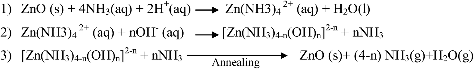 | ||
| Scheme 1 Reaction mechanism for the formation of ZnO semiconductor film. | ||
The structural properties of the samples were investigated by X-ray diffraction using CuKα radiation (λ = 1.5406 Å). We used scanning electron microscopy (SEM) and atomic force microscopy (AFM) for surface morphology imaging. Photoluminescence (PL) spectra were recorded at 266 nm and 375 nm excitation wavelengths. Time-resolved photoluminescence (TRPL) measurements were carried out using a pulsed diode laser (375 nm) with an excitation power of 35 mW. The diode laser exhibits laser pulse durations of 80 ps and a repetition rate of 90 MHz. Reflectance measurements were measured with a spectrophotometer equipped with an integrating sphere. The integrating sphere collects all the reflected light (both specular and diffuse reflectance) over a wavelength range of 200–800 nm.
3. Results and discussions
Prior to ZnO film deposition, the surface of the freshly etched porous GaAs substrate was treated in 1 M sodium carbonate solution (Na2CO3) for 12 s. We previously reported that Na2CO3 remove any oxide layer formed during anodization process.17,18 The porosity of the layer, as determined by weight measurements, is 58%. Fig. 1 shows SEM images in both cross-section (Fig. 1a) and plan (Fig. 1b) views of the cleaned porous GaAs layer. As we can see, pores with sizes in range of about 10–40 nm were obtained over the porous GaAs surface. The process of etching in (100) GaAs formed pores oriented along 〈111〉B crystallographic direction.19–21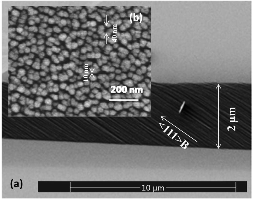 | ||
| Fig. 1 SEM micrographs showing the morphology of porous GaAs layer in both (a) cross-section and (b) plane views of the porous GaAs. | ||
The crystalline quality of the porous layer is of major importance for ZnO films deposition. Fig. 2 shows XRD ω-scan profiles for the flat GaAs substrate (Fig. 2a), the porous GaAs layer (Fig. 2b) and the porous layer treated with Na2CO3 (Fig. 2c). The XRD rocking curve measurements were performed for the (400) reflections. The XRD spectrum of the flat GaAs shows a sharp peak at ω = 33.02°. The porous GaAs peak shifts to higher angle due to a compressive out-of-plane strain in the porous layer. Upon cleaning treatment, the relative peak shift is clearly reduced and the compressive strain decreased from −2.33 × 10⁻² to −2.68 × 10⁻⁴, resulting in an enhanced crystalline property of the porous GaAs substrate, which is desired for ZnO film deposition.
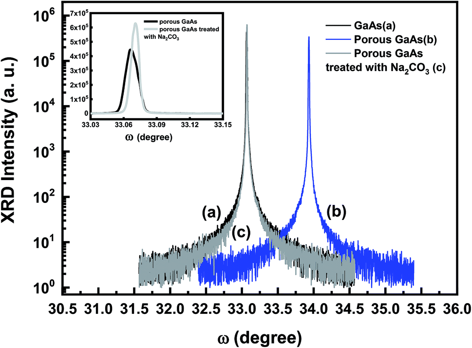 | ||
| Fig. 2 XRD rocking curve measurements for the (400) reflections of GaAs (a), porous GaAs (b), and the cleaned porous GaAs by Na2CO3 (c). The inset shows the zoom of spectra corresponding to samples (a) and (c), plotted in linear scale. | ||
The PL spectrum of the anodized GaAs after chemical cleaning is presented in Fig. 3. For comparison, the PL spectrum of the flat GaAs substrate is also shown in the inset of Fig. 3. The PL spectra of GaAs and porous GaAs are peaked at 810 nm (1.53 eV) and 543 nm (2.28 eV), respectively. The peak position of the heavily doped GaAs substrate (p = 2 × 1018 cm−3) is higher than that of the undoped GaAs (1.424 eV) due to band filling effect.22 Visible PL emissions from porous GaAs were previously observed by many authors and assigned to arsenic and gallium oxides micro-crystals23 or to quantum confinement effect in GaAs nanocrystallites.24 As we have removed oxides from the porous GaAs surface, we ascribed the visible PL to a quantum size effect in GaAs nanocrystallites. The broad PL band of porous GaAs layer was deconvoluted into individual Gaussian contributions and the result is shown in Fig. 3. We have identified a cyan, green, and orange emission bands peaked at 517 nm, 545 nm and 588 nm, respectively.
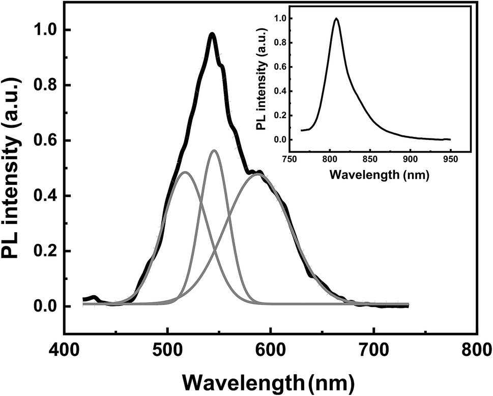 | ||
| Fig. 3 Room temperature PL spectrum and deconvoluted PL spectra (gray solid lines) for porous GaAs. In the inset, the PL spectrum of the heavily doped GaAs substrate is shown for comparison. | ||
For structural characterization of ZnO/porous GaAs, an XRD analysis was carried out in the 10°–80° range of 2θ. Fig. 4 shows the diffraction spectra of ZnO/porous GaAs and porous GaAs for comparison. The porous GaAs substrate exhibit an XRD spectrum peaked at 66.1° characteristic of (400) diffraction of monocrystalline GaAs. The XRD spectrum of ZnO/porous GaAs shows two diffraction peaks having a strong asymmetry. The insets in the Fig. 4 show the zoomed part of the scan around 2θ = 31.4° and 66°. The XRD spectra were fitted with Gaussian functions using four peaks at 2θ = 31.43°, 34.5°, 65.85°, and 66.03°. Based on the analytical results, the diffraction peaks at 2θ = 31.5° and 61.03° were identified to be the (200) and (400) diffraction peaks of GaAs. The diffraction peak corresponding to (200) was not observed for porous GaAs layer and appear after deposition of ZnO film. The (400) porous GaAs diffraction peak shifts to lower angle after ZnO deposition. This result reveals a tensile out-of-plane strain due to lattice parameter increase in the porous layer growth direction. The diffraction peaks at 2θ = 31.43° and 65.85° are identified as (100) and (200) planes of the ZnO wurtzite (hexagonal) structure. From the XRD patterns, we notice that the ZnO film have monocrystalline structure with a-axis orientation. Generally, ZnO crystallizes in a wurtzite type structure in polar (c-oriented) and non-polar (a-oriented) planes.26,27 In this work, ZnO deposited on porous GaAs substrate shows no diffraction peak related to the orientation of the c(002) polar axis, which is beneficial for efficient optoelectronics applications.28 It has been revealed that ZnO growth in a non-polar direction allows the fabrication of electrostatic field-free structures, which improves quantum efficiency.29 Very few reports were found on the growth of ZnO films directed at the a-axis.30 This work confirms a-axis oriented ZnO/porous GaAs film using the spin-coating process which is cost-effective.
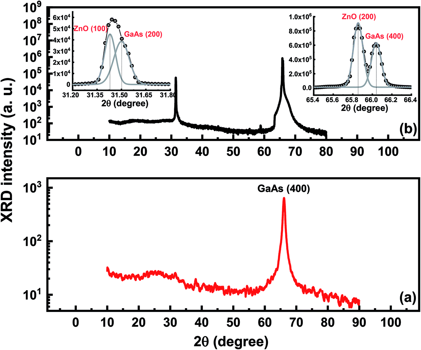 | ||
| Fig. 4 X-ray diffraction spectra of porous GaAs (a) and ZnO/porous GaAs (b). The insets in (a) show the zoomed part of the scan around 2θ = 31.4° and 66°, plotted in linear scale. | ||
According to the Bragg equation, the lattice constant a for the ZnO film, oriented along (100) crystallographic direction, can be calculated:31
 | (1) |
The lattice strain (ε) in ZnO/porous GaAs can be calculated using the tangent formula:32
 | (2) |
Fig. 5 presents 3D AFM images for scanning square area of 2 × 2 μm2 as well as the respective plots of the height distribution histograms of ZnO films. Fig. 5b shows that porous GaAs substrate is beneficial to deposit uniform array of ZnO nanostructures having nanotips-like morphology. Most of the peaks show very narrow height distribution around the mean height (![[h with combining macron]](https://www.rsc.org/images/entities/i_char_0068_0304.gif) = 0). However, ZnO/GaAs (Fig. 5a) exhibit considerable dispersion of peak heights, ranging between −40 to 40 nm, which is due to the presence of occasional high peaks on the surface caused by the formation of larger-sized ZnO clusters. Fig. 6 shows 2D AFM images and cross-sectional profiles. The results compared to those formed on GaAs substrate reveal that the average size of ZnO nano-crystallites is about 12 nm on porous GaAs and ranges from 49 nm to 411 nm on GaAs, approximately.
= 0). However, ZnO/GaAs (Fig. 5a) exhibit considerable dispersion of peak heights, ranging between −40 to 40 nm, which is due to the presence of occasional high peaks on the surface caused by the formation of larger-sized ZnO clusters. Fig. 6 shows 2D AFM images and cross-sectional profiles. The results compared to those formed on GaAs substrate reveal that the average size of ZnO nano-crystallites is about 12 nm on porous GaAs and ranges from 49 nm to 411 nm on GaAs, approximately.
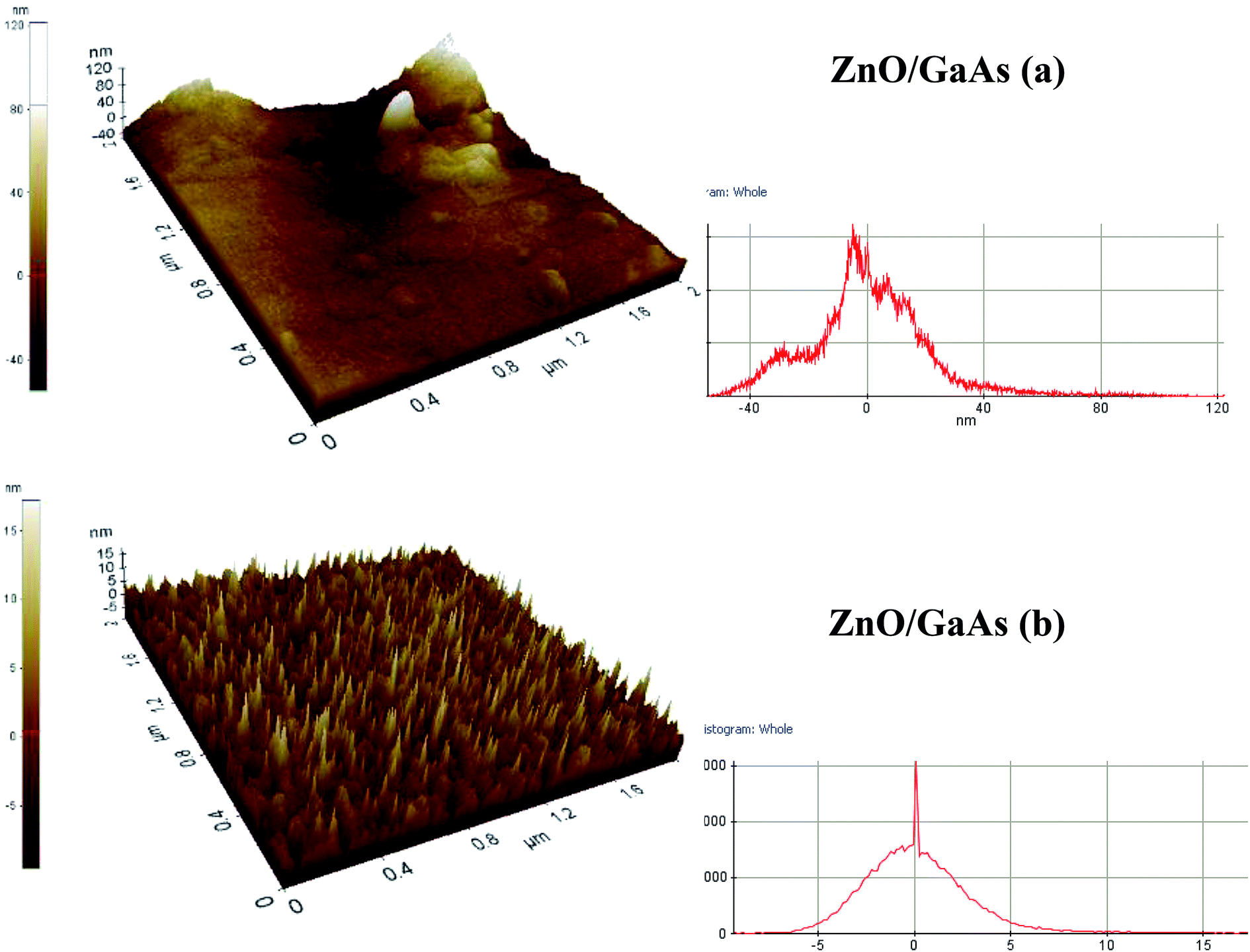 | ||
| Fig. 5 3D AFM images and height distribution histograms for ZnO/GaAs (a) and ZnO/porous GaAs (b). | ||
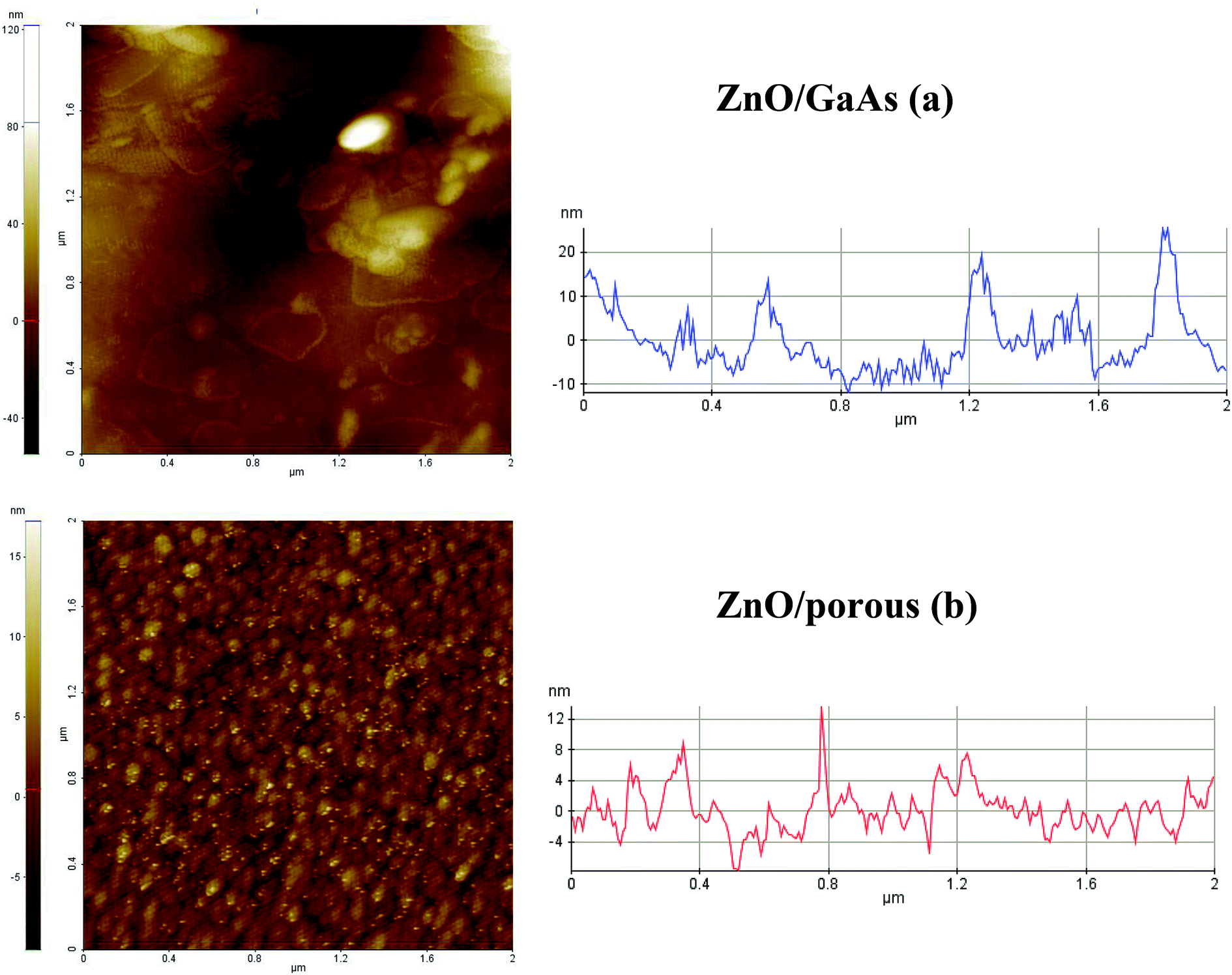 | ||
| Fig. 6 2D AFM images and height profiles for ZnO/GaAs (a) and ZnO/porous GaAs (b). | ||
The roughness parameters that directly control many physical and chemical properties of ZnO films were also determined. We found that GaAs substrate is beneficial to decrease the average roughness (Ra) from 26 nm to 2 nm. The root mean square of roughness (Rq) of the surface decreases from 34 nm to 2.6 nm. Rz averages the five highest peaks and the five deepest valleys relative to the reference plane. The lowest Rz value of 12 nm measured for ZnO/porous GaAs indicates a smooth ZnO surface having less occasional extremes. However, the absence of substrate porosity results in Rz = 126 nm for ZnO/GaAs due to extreme peaks and valleys that are present on the surface.
The total reflectance spectra of ZnO/GaAs and ZnO/porous GaAs surfaces are shown in Fig. 7 over a wavelength range of 200–800 nm. The reflectance spectra of GaAs and porous GaAs substrates are also shown for comparison. ZnO films show significantly lower refectance compared with GaAs and porous GaAs substrates. This indicates that ZnO films exhibit anti-reflection behavior. Better anti-reflection performance is obtained when the ZnO is deposited on the porous GaAs substrate. This behaviour can be attributed to differences in the ZnO surface morphology discussed above. As reported by Y. C. Chang,34 the morphology of ZnO nanostructures with sharp tip exhibit a gradual decrease of refractive index from the surface, resulting in superior antireflection property.
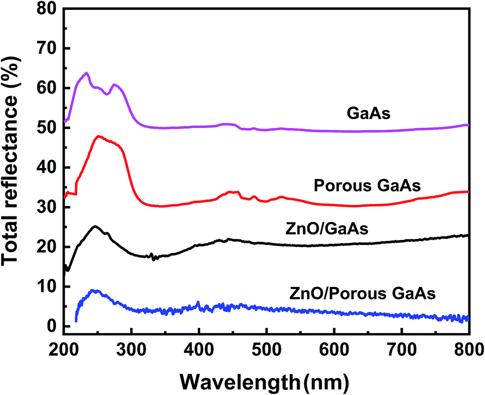 | ||
| Fig. 7 Total reflectance spectra for GaAs, porous GaAs, ZnO/GaAs and ZnO/porous GaAs measured using an integrating sphere. | ||
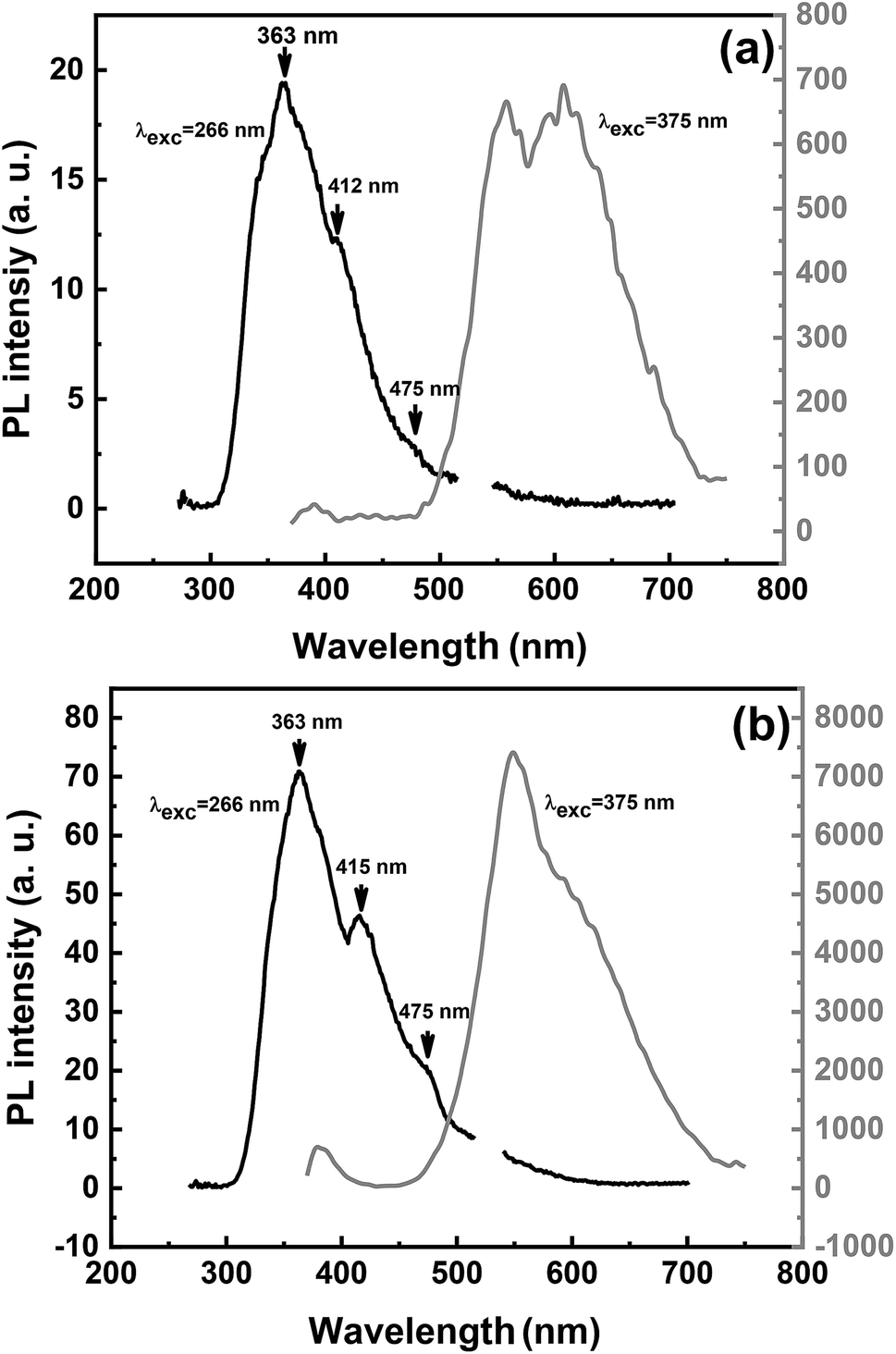
Fig. 8 shows the PL spectra of ZnO/GaAs and ZnO/porous GaAs measured at room temperature using an excitation wavelength λexc = 375 nm. The as-deposited ZnO films show broadband emission covering most of the visible spectral region (450–750 nm). For deeper investigation, we deconvoluted the PL spectra into individual Gaussian contributions. The results illustrated in Fig. 8 prove that the PL spectra are composed of green and orange emissions peaked at 545 nm (2.27 eV) and 597 (2.07) for ZnO/porous GaAs, and at 547 nm (2.26 eV) and 608 nm (2.04 eV) for ZnO/GaAs. For ZnO/GaAs, there is no contribution from GaAs substrate to the visible-band, but only from the ZnO related emission. The contribution of porous GaAs luminescence to the PL spectrum of ZnO/porous GaAs cannot be neglected since green and orange emissions peaked at 545 nm and 588 nm were also observed for porous GaAs substrate. Thus, the visible emission observed for ZnO/porous GaAs could be explained by considering two contributions: ZnO and porous GaAs PL responses. In an effort to quantify the PL spectra, we calculated the peak intensity ratio R of ZnO/porous GaAs to ZnO/GaAs for the green and the orange emissions. The R value is equal to 13 and 7 for the green and orange emissions, respectively. These results reveal that the porosity of GaAs substrate is beneficial to enhance the visible PL intensity of ZnO.
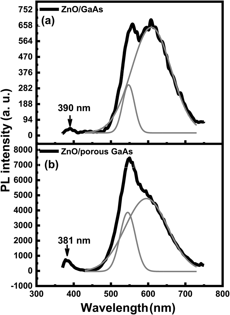 | ||
| Fig. 8 Room temperature PL spectra and deconvoluted PL spectra (gray solid lines) for ZnO/GaAs (a) and ZnO/porous GaAs (b). | ||
A number of studies on the optical properties of ZnO nanostructures have reported that the green and orange emissions can be assigned to oxygen vacancies (VO), oxygen interstitials (Oi) and zinc interstitials (Zni).35–40 According to L. S. Vlasenko et al.,35 electron paramagnetic-resonance analysis proved that the green emission is composed of two transitions, with electron–hole recombinations from conduction band to oxygen vacancy level and from zinc interstitial level to oxygen vacancy level. The Zni and VO levels are located at 0.22 eV and 2.47 eV slightly below the conduction band as previously determined experimentally by E. G. Bylander36 and J. Čížek et al.,37 respectively. Therefore, it is expected that the energy interval between the Zni level and the VO level is approximately 2.25 eV. This is well consistent with the green peaks that are centered at 2.26 (547 nm) and 2.27 eV (545 nm). Using full-potential linear muffin–tin orbital method,38 the position of the Oi level is located at 2.28 eV below the conduction band. Therefore, the calculated band transition from Zni to Oi level is approximately 2.06 eV. This value is close to the orange peaks centered at 2.07 eV (597 nm) and 2.04 eV (608 nm), as shown in Fig. 11.
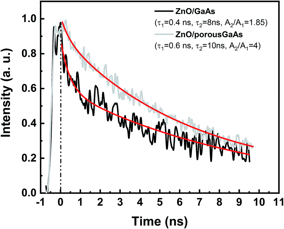
Fig. 8 shows a weak UV response peaked at 390 nm for ZnO/GaAs and at 381 nm for ZnO/porous GaAs. According to reviewed papers, the PL peak of ZnO varying from 373 to 390 nm have been assigned to near band gap emission in ZnO nanostructures.41–43 To further clarify the origin of the UV emissions, time resolved photoluminescence (TRPL) experiments were performed in the picoseconds time scale. TRPL spectra are presented in Fig. 9 for ZnO/GaAs and ZnO/porous GaAs. The PL time decay for the two samples can be fitted by:
 | (3) |
 | ||
| Fig. 9 Time-resolved PL decay curves of ZnO/GaAs and ZnO/porous, respectively, measured at 375 nm. The solid lines represent fitting curve. | ||
It is worth noting that UV emissions observed for ZnO/GaAs and ZnO/porous GaAs exhibit very low intensities, compared to visible emissions. The ratio of intensities of ultraviolet and visible emission (IUV/IVisible) is considered as an important factor used to compare the optical properties of materials. According to I. B. Olenych et al.,49 the decrease in wavelength of UV excitation radiation of ZnO film induces enhancement of short-wavelength photoluminescence intensity. For deeper investigations, the photoluminescence of ZnO films were measured using λexc = 266 nm, as shown in Fig. 10. The PL spectra of ZnO films using λexc = 375 nm are also shown for comparison. We observe UV peaks at 363 nm for both ZnO/GaAs and for ZnO/porous GaAs that we attribute to band–band transition due to free electrons. Therefore, the porosity of GaAs substrate introduces no change on the ZnO band gap because confinement effects could not be considered due to very small Bohr radius of ZnO. The violet emission observed at 412–415 nm (∼3 eV) for ZnO/GaAs and ZnO/porous GaAs is attributed to the electron transition from the bottom of the conduction band to the Zn vacancy level. According to P. S. Xu et al.,38 the calculated energy interval from the bottom of the conduction band to the Zn vacancy (VZn) level is 3.06 eV. This value agrees well with the energies 2.98–3 eV of the violet emissions peaked at 412–415 nm in this study. In addition to violet emission, blue emission has been observed at 475 nm (2.61 eV) in both the samples. Recently, D. Das et al.50 observed blue luminescence from ZnO nanoparticles peaked at 467 nm (2.66 eV). This transition was assigned to electron transition from the conduction band to oxygen antisite (OZn) level. The blue emission observed at 475 nm (2.61 eV) for ZnO/GaAs and ZnO/porous GaAs is very close to 2.66 eV and a possible mechanism related with oxygen antisite defect level as final state can be suggested.
 | ||
| Fig. 10 PL spectra measured using λexc = 266 nm and λexc = 375 nm for ZnO/GaAs (a) and ZnO/porous GaAs (b). | ||
From the experimental results, we propose two mechanisms leading to PL emissions (illustrated in Fig. 11): the typical exciton emission or near-band-edge emission and the defect related deep level emissions in the visible region. The PL spectra of ZnO films recorded at 266 nm excitation wavelength exhibit a shift in PL maxima to smaller wavelengths (blue shift) with a broad emission peak, while the green and orange band edge emissions are strongly quenched. We suggest that, when ZnO film is excited using λexc = 375 nm, only a few electrons get to near-conduction band and may recombine directly or through interface states, while most of them are trapped at defect states. As a result, emissions in the visible spectral region are observed and the reduced UV luminescence could be explained by the limited recombination process of electron–hole pairs from the near-conduction band. For the λexc = 266 nm, the intensity of band–band emission increase significantly as compared to the green and orange emissions, which are quenched to the noise level.
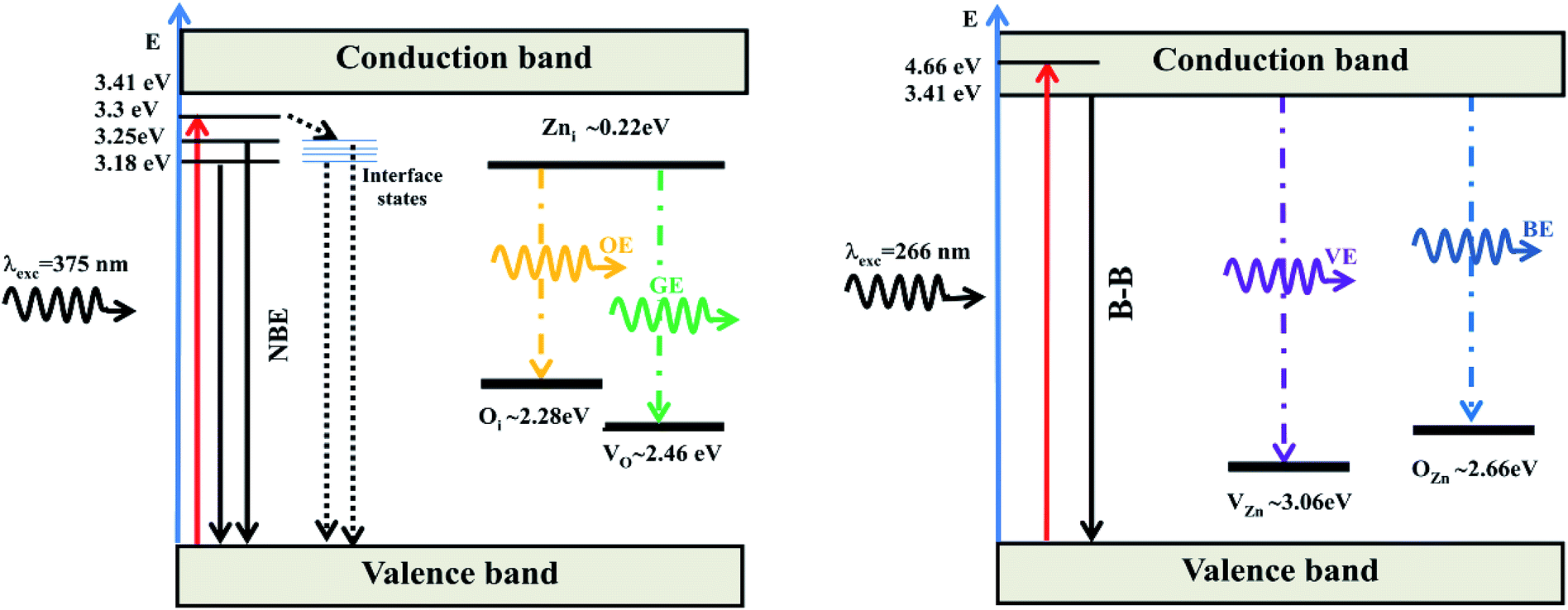 | ||
| Fig. 11 Schematic band diagrams showing two mechanisms leading to PL emissions: the typical exciton (B–B) or near-band-edge (NBE) emissions and the defect related deep level emissions based on the reported data as described in ref. 35–39 and 50. The schematic band diagrams are shown for two excitation wavelengths (λexc = 375 nm and for λexc = 266 nm). OE: orange emission, GE: green emission, VE: violet emission and BE: blue emission. | ||
The UV emission peak at 363 nm observed for ZnO/porous GaAs has fourfold increase as compared to that of ZnO/GaAs. As discussed above, the porosity of GaAs substrate is beneficial to enhance the visible PL intensity of ZnO as well. Naddaf et al.16 have reported an increase of visible PL intensity of ZnO films grown by RF magnetron sputtering when porous GaAs is used as a substrate. The authors demonstrated a strong relationship with the change in the content of zinc and oxygen related defects in the film. In this work, we have shown that the surface morphology of ZnO/porous GaAs has the ability to minimize light reflection in the UV-Vis spectral range. This lets us to conclude that ZnO/porous GaAs has the advantage to absorb more light, resulting in an efficient photoluminescence.
4. Conclusion
A low cost and facile approach was adapted to deposit ZnO thin films onto GaAs and porous GaAs substrates. XRD analysis confirms the monocrystalline structure of ZnO/porous GaAs with a-axis-preferred orientation. Atomic force microscopy studies reveal that the porosity of GaAs is beneficial to grow ZnO nanostructures with sizes down to 12 nm and a surface roughness as low as 2.6 nm. The photoluminescence measurements prove that ZnO films exhibit typical excitation wavelength dependence. Enhancement in photoluminescence intensity in UV-visible regions was also observed for ZnO/porous GaAs compared to ZnO/GaAs. As a result, ZnO nanostructures grown on porous GaAs have high potential for advanced devices such as photodetectors.Conflicts of interest
There are no conflicts to declare.References
- E. Topoglidis, A. E. G. Cass, B. O'Regan and J. R. Durrant, J. Electroanal. Chem., 2001, 517, 20–27 CrossRef CAS.
- Z. L. Wang, J. Phys.: Condens. Matter, 2004, 16, 829–858 CrossRef.
- T. Yang, Y. Li, M. Y. Zhu, Y. B. Li, J. Huang, H. M. Jin and Y. M. Hu, Mater. Sci. Eng. B, 2010, 170, 129–132 CrossRef CAS.
- N. Lehraki, M. S. Aida, S. Abed, N. Attaf, A. Attaf and M. Poulain, Curr. Appl. Phys., 2012, 12, 1283–1287 CrossRef.
- M. C. Sportelli, M. A. Nitti, M. Valentini, R. A. Picca, E. Bonerba, L. Sabbatini, G. Tantillo, N. Cioffi and A. Valentini, Sci. Adv. Mater., 2014, 6, 1019–1025 CrossRef CAS.
- R. O. Ndong, H. E. Obame, Z. H. Moussambi and N. Koumba, Journal of Theoretical and Applied Physics, 2018, 12, 309–317 CrossRef.
- S. Park, C.-H. Kima, W. J. Lee, S. Sunga and M. H. Yoon, Mater. Sci. Eng., R, 2017, 144, 1–22 CrossRef.
- S. Y. Park, K. Kim, K. H. Lim, E. Lee, S. Kim, H. Kim and Y. S. Kim, RSC Adv., 2013, 3, 21339–21342 RSC.
- Y. Jin, J. Wang, B. Sun, J. C. Blakesley and N. C. Greenham, Nano Lett., 2008, 8, 1649–1653 CrossRef CAS PubMed.
- M. H. Mamata, Z. Khusaimi, M. Z. Musa, M. F. Maleka and M. Rusopa, Sens. Actuators, A, 2011, 171, 241–247 CrossRef.
- S. T. Meyers, J. T. Anderson, C. M. Hung, J. Thompson, J. F. Wager and D. A. Keszler, J. Am. Chem. Soc., 2008, 130, 17603–17609 CrossRef CAS PubMed.
- O. Marin, G. grinblat, A. M. Gennaro, M. Tirado, R. R. Koropecki and D. Comedi, Superlattices Microstruct., 2015, 79, 29–37 CrossRef CAS.
- E. Kayahan, J. Lumin., 2010, 130, 1295–1299 CrossRef CAS.
- M. S. Kim, K. G. Yim, S. Kim, G. Nam and J. Y. Leem, J. Sol-Gel Sci. Technol., 2011, 59, 364–370 CrossRef CAS.
- M. B. Bouzouraa, A. En Naciri, A. Moadhen, H. Rinnert, M. Guendouz, Y. Battie, A. Chaillou, M. A. Zaïbi and M. Oueslati, Mater. Chem. Phys., 2016, 175, 233–240 CrossRef CAS.
- M. Naddaf and M. Saad, Vacuum, 2015, 122, 36–42 CrossRef CAS.
- A. Lebib, E. Ben Amara and L. Beji, J. Lumin., 2017, 188, 337–341 CrossRef CAS.
- S. B. Khlifa, B. Gruzza, C. Robert-Goumet, G. Bremond, M. Hjiri, F. Saidi, L. Bideux, L. Béji and H. Maaref, J. Lumin., 2008, 128, 1611–1616 CrossRef.
- H. Föll, S. Langa, J. Carstensen, M. Christophersen and I. M. Tiginyanu, Adv. Mater., 2003, 15, 183–189 CrossRef.
- V. Kochergin and M. Christophersen, Appl. Phys. Lett., 2005, 86, 042108 CrossRef.
- S. Langa, J. Carstensen, M. Christophersen, H. Foll and I. M. Tiginyanu, Appl. Phys. Lett., 2001, 78, 1074 CrossRef CAS.
- B. E. Sernelius, Phys. Rev. B: Condens. Matter Mater. Phys., 1986, 33, 8582–8586 CrossRef CAS PubMed.
- M. Naddaf, J. Mater. Sci.: Mater. Electron., 2017, 28, 16818–16825 CrossRef CAS.
- M. Naddaf and M. Saad, J. Mater. Sci.: Mater. Electron., 2013, 24, 2254–2263 CrossRef CAS.
- J. Sabataityte, I. Simkiene, R.-A. Bendorius, K. Grigoras, V. Jasutis, V. Pacebutas, H. Tvardauskas and K. Naudzius, Mater. Sci. Eng. C, 2002, 19, 155–159 CrossRef.
- V. A. Coleman and C. Jagadish, in Zinc Oxide Bulk, Thin Films and Nanostructures, ed. C. Jagadish and S. Pearton, Elsevier, 2006, p. 1 Search PubMed.
- L. P. Dai, H. Deng, G. Chen, C. F. Tang, M. Wei and Y. Li, Vacuum, 2007, 81, 969–973 CrossRef CAS.
- M. P. Bhole and D. S. Patil, J. Optoelectron. Adv. Mater., 2007, 1, 672–676 CAS.
- P. waltereit, O. Brandt, A. Tranpert, H. Grahn, J. Menniger, M. Ramsteiner, M. Reiche and K. H. Ploog, Nature, 2000, 406, 865–867 CrossRef CAS PubMed.
- U. Neumann, R. Grunwald, U. Griebner and G. Steinmeyer, Appl. Phys. Lett., 2005, 87, 171108 CrossRef.
- T. P. Rao and M. C. Santhoshkumar, Appl. Surf. Sci., 2009, 255, 7212–7215 CrossRef.
- P. P. Sahay and R. K. Nath, Sens. Actuators, B, 2008, 134, 654–659 CrossRef CAS.
- K. A. Alim, V. A. Fonoberov, M. Shamsa and A. A. Balandin, J. Appl. Phys., 2005, 97, 124313 CrossRef.
- Y. C. Chang, RSC Adv., 2014, 4, 56241–56247 RSC.
- L. S. Vlasenko and G. D. Wathins, Phys. Rev. B: Condens. Matter Mater. Phys., 2005, 71, 125210 CrossRef.
- E. G. Bylander, J. Appl. Phys., 1978, 49, 1188–1195 CrossRef CAS.
- J. Čížek, J. Valenta, P. Hruška, O. Melikhova and I. Procházka, Appl. Phys. Lett., 2015, 106, 251902 CrossRef.
- P. S. Xu, Y. M. Sun, C. S. Shi, F. Q. Xu and H. B. Pan, Nucl. Instrum. Methods Phys. Res., 2003, 199, 286–290 CrossRef CAS.
- B. Lin, Z. Fu and Y. Jia, Appl. Phys. Lett., 2001, 79, 943 CrossRef CAS.
- Lv. Jinpeng and Li. Chundong, Appl. Phys. Lett., 2013, 103, 232114 CrossRef.
- R. C. Wang, C. P. Liu, J. L. Huang and S. J. Chen, Appl. Phys. Lett., 2005, 87, 053103 CrossRef.
- D. Zhao, C. Andreazza, P. Andreazza, J. Ma, Y. Liu and D. Shen, Chem. Phys. Lett., 2004, 399, 522–526 CrossRef CAS.
- Q. Yang, K. Tang, J. Zuo and Y. Qian, Appl. Phys. A, 2004, 79, 1847–1851 CrossRef CAS.
- W. Yu, X. Li and X. Gao, Cryst. Growth Des., 2005, 5, 151–155 CrossRef CAS.
- W. Chebil, A. Fouzri, A. Fargi, B. Azeza, Z. Zaaboub and A. Sallet, Mater. Res. Bull., 2015, 70, 719–727 CrossRef CAS.
- S. Hong, T. Joo, W. I. Park, Y. H. Jun and G.-C. Yi, Appl. Phys. Lett., 2003, 83, 4157–4159 CrossRef CAS.
- S. Yamamoto, H. Yano, T. Mishina and J. Nakahara, J. Lumin., 2007, 126, 257–262 CrossRef CAS.
- H. Zhou, H. Alves and D. M. Hofmann, Phys. Status Solidi B, 2002, 229, 825–828 CrossRef CAS.
- I. B. Olenych, L. S. Monastyrskii and A. P. Luchechko, J. Appl. Spectrosc., 2017, 84, 66–70 CrossRef CAS.
- D. Das and P. Mondal, RSC Adv., 2014, 4, 35735–35743 RSC.
| This journal is © The Royal Society of Chemistry 2019 |