DOI:
10.1039/C9RA04470A
(Paper)
RSC Adv., 2019,
9, 25216-25224
Strain induced valley degeneracy: a route to the enhancement of thermoelectric properties of monolayer WS2†
Received
14th June 2019
, Accepted 5th August 2019
First published on 13th August 2019
Abstract
Two-dimensional transition metal dichalcogenides show great potential as promising thermoelectric materials due to their lower dimensionality, the unique density of states and quantum confinement of carriers. Here the effects of mechanical strain on the thermoelectric performances of monolayer WS2 have been investigated using density functional theory associated with semiclassical Boltzmann transport theory. The variation of the Seebeck coefficient and band gap with applied strain has followed the same type of trend. For n-type material the relaxation time scaled power factor (S2σ/τ) increases by the application of compressive strain whereas for p-type material it increases with the application of tensile strain due to valley degeneracy. A 77% increase in the power factor has been observed for the n-type material by the application of uniaxial compressive strain. A decrease in lattice thermal conductivity with the increase in temperature causes an almost 40% increase in ZT product under applied uniaxial compressive strain. From the study, it is observed that uniaxial compressive strain is more effective among all types of strain to enhance the thermoelectric performance of monolayer WS2. Such strain induced enhancement of thermoelectric properties in monolayer WS2 could open a new window for the fabrication of high-quality thermoelectric devices.
Introduction
Low dimensionality of materials opens a new window to enhance thermoelectric properties due to their unique density of states (DOS) and the quantum confinement effect. Due to the unique layered structure, two dimensional (2D) materials have attracted much attention. The first synthesized 2D layered material graphene is well known for its very high mobility but opening a reasonable band gap in graphene is still a challenging problem.1 Therefore 2D transition metal dichalcogenides (TMDCs) came into the picture owing to their tunable bandgap, high electrical mobility, low thermal conductivity, chemical stability, etc.2 The fantastic combination of electrical and thermal transport in these 2D materials can lead to a significantly large thermoelectric figure of merit (ZT). TMDCs show a great potential in thermoelectric application to convert waste heat to electricity because of their high electrical conductivity and low thermal conductivity. Theoretical calculation of the thermoelectric properties of monolayer TMDCs suggests that the ZT product of these materials is generally low3 as compared to well-known thermoelectric materials such as Bi2Te3 and Bi2Se3.4 Various efforts like chemical doping and functionalization,5 strain engineering,6 defect engineering,7 making heterostructures8 have been taken into consideration to enhance the thermoelectric properties. Among these strain engineering is one of the most popular methods to tune the electronic and thermoelectric properties of these materials.
The effect of layer numbers on the thermoelectric power factor (PF) and ZT product has been predicted theoretically for MoS2, MoSe2, WS2 and WSe2 and the enhancement of ZT product in TMDCs is due to the increased degeneracy of the band edges.9,10 High ZT value close to 1 has been predicted in suspended monolayer and bilayer MoS2 which is much higher than that of bulk suggests that low dimensionality may be a possible way to enhance the thermoelectric properties.11 By layer mixing or forming heterostructures of different TMDCs thermoelectric performance is enhanced due to increased DOS and reduction of band gap near the Fermi level.12,13 Theoretical calculation predicted the value of lattice thermal conductivity (kph) of monolayer MoS2 nanoribbon to be 29.2 W m−1 K−1 (ref. 14) which is higher than previous value of 1.35 W m−1 K−1 (ref. 15) but matched closely with experimental value of 34.5 W m−1 K−1.16 Experimental observation of very large power factor of 8.5 m W m−1 K−2 at room temperature in exfoliated few layer MoS2 because of the increased DOS and 2D confinement of electrons near the band edge suggests that 2D TMDCs may turn out to be promising thermoelectric materials. Enhanced thermoelectric properties have been observed both experimentally and theoretically in monolayer MoS2 with applied external electric field due to the change in valley degeneracy.17,18 The effect of mechanical strain on the electronic and vibrational properties in different TMDCs has been investigated theoretically and suggests that TMDCs are very sensitive to mechanical strain19–23 and monolayer MoS2 is dynamically stable up to 15% biaxial tensile strain.24 Enhancement of thermoelectric power factor by the application of compressive strain on monolayer MoS2 has been predicted theoretically and maximum PF has been found for n-type doping with applied 3% uniaxial zigzag compressive strain.25 A 2–4% biaxial tensile strain results a reduction in kph of monolayer suggests that strain engineering could be an effective way to increase ZT product.26 Uniaxial compressive strain induced enhancement of layered oxychalcogenides BiCuOCh (Ch = S, Se and Te) has been predicted and an increment of the power factor by 11.4% by applying −6% compressive strain is also observed.27,28
Though in TMDCs, MoS2 is the most widely studied material a thorough investigation of the role of strain on WS2 is highly warranted. In this work to the best of our knowledge for the first time we have performed a systematic investigation of electronic, vibrational and thermoelectric properties of monolayer WS2 and the effect of different types of strain on electronic and thermoelectric properties of monolayer WS2. We have shown the variation of thermoelectric properties with chemical potential as well as carrier concentration and our study show that both the approaches lead to same results. The first principle calculation shows that the ZT product can be enhanced by 38.5% with applied uniaxial compressive strain and we have found the highest ZT product of 0.72 in monolayer WS2. Such compressive strain induced enhancement of thermoelectric properties in monolayer WS2 can have potential application in thermoelectric devices for the efficient conversion of wastage heat to electricity.
Computational details
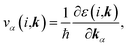
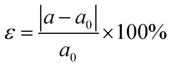
First principles calculation has been performed using density functional theory (DFT) with projector augmented wave (PAW)29 potentials and the Perdew–Burke–Ernzerhof (PBE)30 generalized gradient approximation (GGA)31 as exchange correlation functional in Quantum Espresso (QE) package.32 A sufficient vacuum of 17 Å along C axis was created to avoid the interaction between layers in periodic boundary condition for monolayer of WS2. A 12 × 12 × 1 dense mesh grid was used to optimize the geometry and energy cutoff for the electronic wavefunctions was set to 50 Ry throughout all the calculations. For the density of state (DOS) and thermoelectric parameter calculations a high dense mesh of K points 48 × 48 × 1 was used. The strain is calculated as  where a0 and a are the lattice constant of relaxed and strained structures respectively. For the thermoelectric and transport properties, a semi classical Boltzmann transport theory was used with constant scattering time approximation (CSTA) as implemented in BoltzTrap33 code. In CSTA we assume that scattering time has very less dependency on energy and both the group velocity of carriers and DOS contribute to the transport function. The group velocity (vg) of carriers in a specific band can be described as
| |
 | (1) |
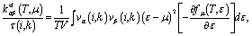
where kα is the αth component of wavevector k and ε(i,k) is the ith energy band and the conductivity tensor can be obtained in terms of group velocity as| | |
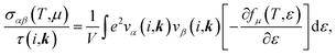
σαβ(i,k) = e2τ(i,k)vα(i,k)vβ(i,k),
| (2) |
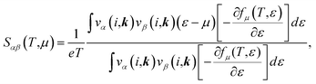
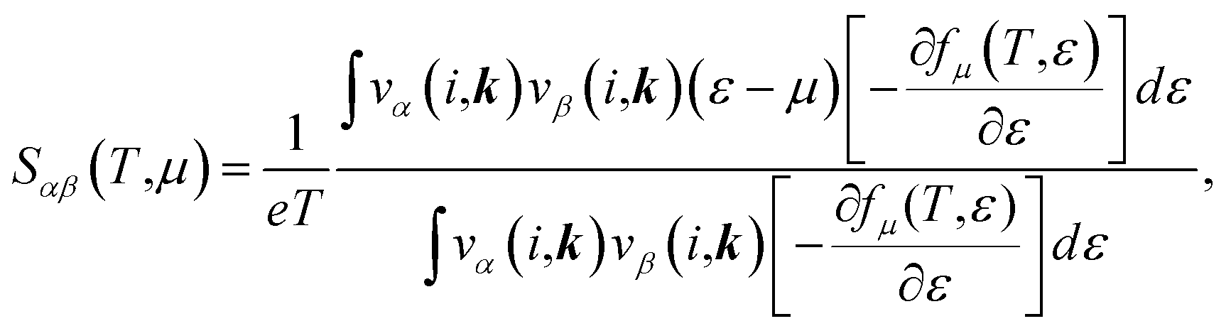
The Seebeck coefficient, electrical conductivity and thermal conductivity due to electron can be calculated by using the values of group velocity vα(i,k) as implemented in BoltzTrap33 code by following equations
| |
 | (3) |
| |
 | (4) |
| |
 | (5) |
where
e,
T,
τ,
μ,
V are electronic charge, temperature, relaxation time, chemical potential, volume of a unit cell respectively and
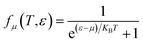
is the Fermi–Dirac distribution function.
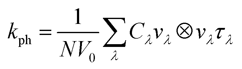
The lattice thermal conductivity (kph) has been calculated with the linearized phonon Boltzmann equation as implemented in Phono3py34 code interfaced with Quantum Espresso (QE) package.32 kph can be expressed as
| |
 | (6) |
where
N,
V0 and
λ are the total number of q points for sampling Brillouin Zone, volume of a unit cell and phonon mode respectively and
Cλ,
vλ and
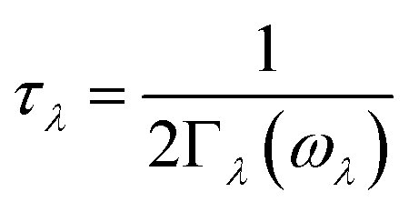
τλ are specific heat, phonon group velocity and phonon lifetime respectively. The phonon lifetime (
τλ) can be expressed as
| |
 | (7) |
where
Γλ(
ω) is known as phonon linewidth and has following form:
| |
 | (8) |
where
ϕ−λλ′λ′′and
nλ are the strength of interaction between three phonons
λ,
λ′ and
λ′′ and phonon occupation number respectively. The detailed calculation can be found elsewhere.
34 For the 2
nd and 3
rd order of interatomic force constant calculation we construct a 2 × 2 × 1 supercell sampled with 6 × 6 × 1 densed
k-point meshes and for the computation of lattice thermal conductivity the reciprocal space of primitive cell was sampled by 20 × 20 × 1
k-point meshes.
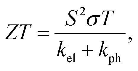
The thermoelectric figure of merit (ZT) has been calculated using the formula
| |
 | (9) |
Where
S,
σ,
T are Seebeck coefficient, electrical conductivity and temperature respectively and
kel and
kph are thermal conductivity due to electron, and lattice thermal conductivity due to phonon respectively.
Results and discussions
Structural parameters
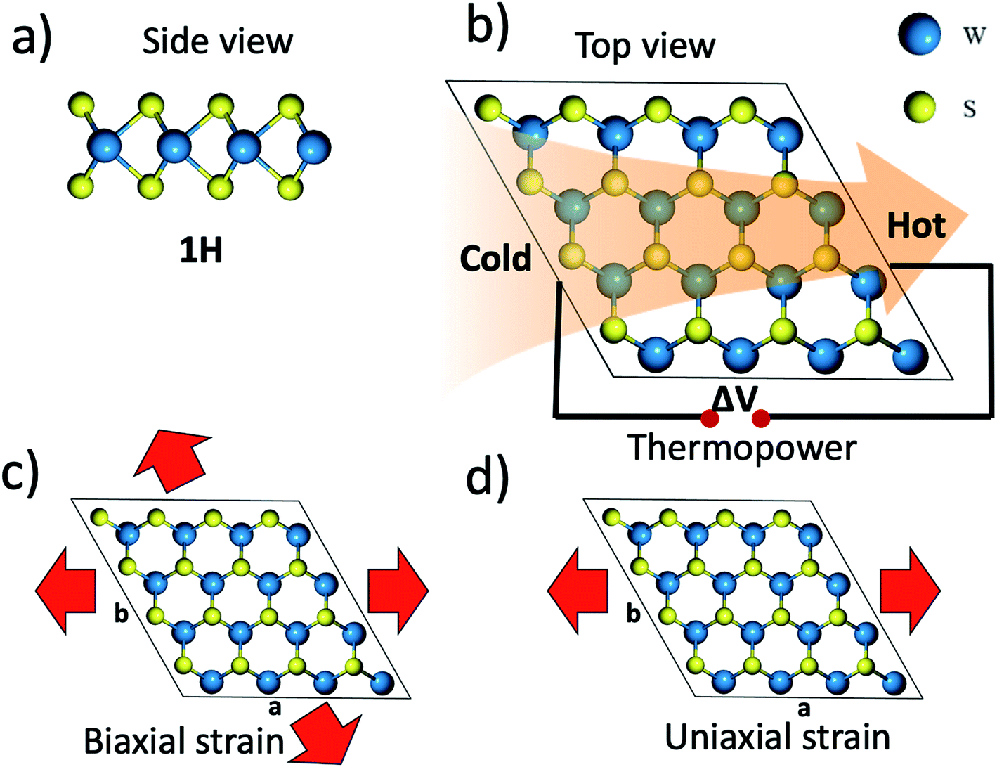
Monolayer WS2 has a hexagonal honeycomb structure belonging to P63/mmc space group with S–W–S layer where W atoms are sandwiched between two layers of S atoms connected with covalent bonds known as 1H phase as shown in Fig. 1a. Bilayer WS2 (2H) consists of two such S–W–S monolayers which are separated by Vander Waals interaction. The optimized lattice constant of a = b = 3.19 Å for a unit cell of monolayer agrees with previous calculations35 and experimental value.36 To apply biaxial strain lattice parameters (a = b = 3.19 Å) are varied up to ±6% in the steps of 1% where + and − signs represent tensile and compressive strain respectively as shown in Fig. 1c. But in case of uniaxial strain we only vary lattice constant “a” up to ±6% while keeping b = 3.19 Å fixed as shown in Fig. 1d.
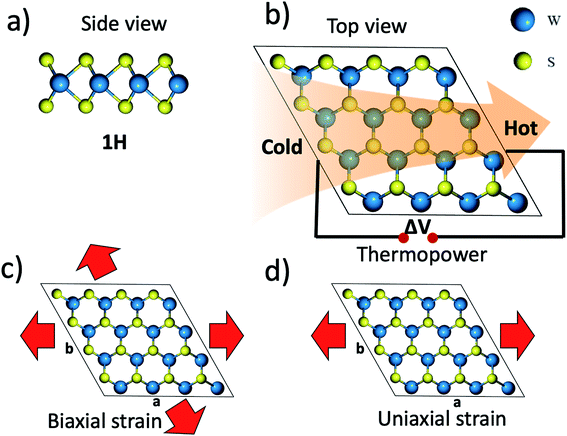 |
| | Fig. 1 Crystal structure of monolayer WS2 (a) side view (b) top view and thermoelectric effect (c) application of biaxial strain (d) application of uniaxial strain. | |
Thermoelectric properties
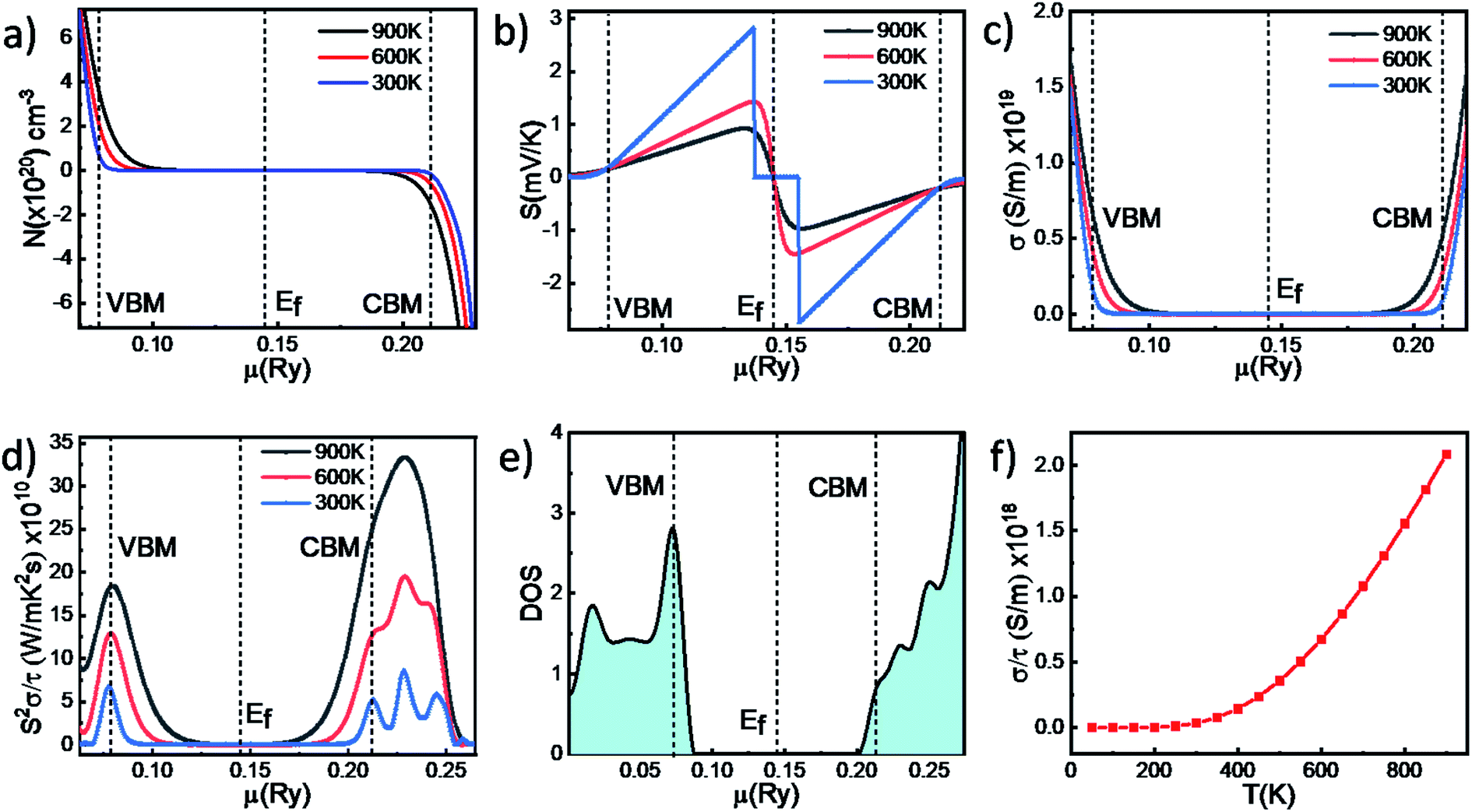
Fig. 2a shows the variation of carrier concentration of the WS2 monolayer with chemical potential at three different temperatures namely 300 K, 600 K and 900 K. Carrier concentration is zero in the band gap region and increases as we go to the band edge. The variation of Seebeck coefficient (S) with chemical potential (μ) shows that very high S value has been observed near the bandgap region as shown on Fig. 2b. S decreases as we go away from band gap region to the valence band and conduction band. This is because as we go away from bandgap region carrier concentration increases as shown in Fig. 2a. And S is inversely proportional to carrier concentration. At 300 K the value of S is 2821 μV K−1 for p-type carriers and 2728 μV K−1 for n-type carriers respectively in monolayer WS2. The S values decreased to 1429 μV K−1 and 1446 μV K−1 at 600 K and 926 μV K−1 and 967 μV K−1 at 900 K for p-type and n-type carriers respectively. At 300 K electrical conductivity is almost zero in the region between the VBM and CBM but it increases at 600 K and 900 K as shown in Fig. 2c. This is due to the increase in the number of carriers at elevated temperatures. Because of high electrical conductivity the thermoelectric power factor (S2σ/τ) has also increased. Fig. 2d shows how thermoelectric power factor S2σ/τ (relaxation time scaled) varies with chemical potential μ(Ry). At 300 K the S2σ/τ is observed to be 5.22 × 10¹⁰ W m−1 K−2 s−1 for n-type carriers (μ > Ef) which increases with temperature and becomes 23.88 × 10¹⁰ W m K−2 s−1 at 900 K. The highest S2σ/τ at 300 K, 600 K, and 900 K are observed to be 8.57 × 10¹⁰ W m−1 K−2 s−1, 19.49 × 10¹⁰ W m−1 K−2 s−1, and 33.35 × 10¹⁰ W m−1 K−2 s−1 for n-type region respectively. The corresponding S2σ/τ at 300 K, 600 K, and 900 K for p-type carriers are 6.77 × 10¹⁰ W m−1 K−2 s−1, 12.90 × 10¹⁰ W m−1 K−2 s−1, and 18.4 × 10¹⁰ W m−1 K−2 s−1 at VBM respectively which are lower than the values obtained for n-type carriers at CBM which indicates that n-type doping is more effective than p-type doping in semiconducting WS2. At 300 K in n-type region there are clearly three peaks in which first peak corresponds to the CBM. As temperature increases the two side peaks convert into two little hump and at 900 K there is one peak corresponding to highest power factor. But no such thing is observed in p-type region. This type of behavior can be explained from DOS near the band edge which is shown in Fig. 2e. Near the valence band edge there is only one peak which corresponds to the energy state at VBM but in conduction band edge there are three humps near the conduction band edge and among them 1st hump corresponds to the CBM at 0.211 Ry and the second hump at 0.228 Ry corresponds to the highest S2σ/τ value near the conduction band edge. As transport takes place near the band edge, we only check the peaks near the valence and conduction band edges. The variation of relaxation time scaled electrical conductivity i.e. σ/τ with temperature shows the semiconducting behavior of WS2 and can be seen in Fig. 2f.
 |
| | Fig. 2 Variation of (a) carrier concentration (b) Seebeck coefficient (S) (c) electrical conductivity (σ/τ) (d) relaxation time scaled thermoelectric power factor (S2σ/τ) as a function of chemical potential μ (Rydberg unit). The dotted lines represent the valence band maximum (VBM), Fermi energy (Ef) and conduction band minimum (CBM) respectively (e) the density of states (DOS) as a function of chemical potential (f) variation of electrical conductivity with temperature in monolayer WS2. | |
We have also shown the variation of Seebeck coefficient, S2σ/τ, σ/τ and Kel as a function of carrier concentration (N) (ESI Fig. S1†) and our results suggest that these values are similar to that calculated from chemical potential approach.
Effect of Bi-axial strain
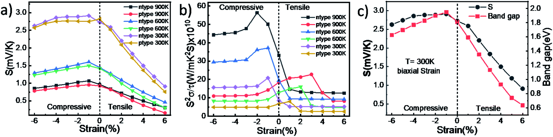
Before studying the role of strain on various thermoelectric properties of WS2 the stability of the structure was validated from the cohesive energy calculations37 by varying the strain on the material. The detail of which is given in Fig. S7 of the ESI.† The variation in Seebeck coefficient with applied biaxial strain (tensile and compressive) for n-type and p-type doping at 300 K, 600 K and 900 K is shown in Fig. 3a. In case of biaxial compressive strain (BCS) the value of S increases as we apply higher strain up to a point and after that point S starts decreasing. This behavior is observed for both p-type and n-type carriers, but S has higher value for n-type carriers than p-type carriers. The highest value obtained at 1% of BCS is 1067 μV K−1 for n type and 955 μV K−1 for p-type at 900 K. But S decreases with application of biaxial tensile strain (BTS) for both types of carrier. The variation of band gap with applied strain follows the same trend as that of the Seebeck coefficient and is shown in Fig. 3c as described by Goldsmid–Sharp relation38 given by the formula, Eg = 2e|Sm|Tm where Sm is the highest Seebeck coefficient, Tm is the corresponding temperature and Eg is the band gap. If we look at the electronic band structure of single layer WS2 (ESI Fig. S2b†) it is clearly seen that at 1% BCS band gap is highest and remains direct and after 2% BCS it starts to decrease and becomes indirect. This is the reason for higher values of Seebeck coefficient at 2% BCS. But for BTS band gap decreases and becomes indirect at 1% BTS and as BTS increases band gap decreases rapidly by going to the point of semiconducting to metal transition at 10% of BTS (ESI Fig. S2g†). That is why Seebeck coefficient decreases by the application of BTS.
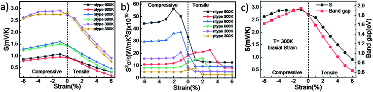 |
| | Fig. 3 Variation in (a) Seebeck coefficient and (b) S2σ/τ with applied both biaxial compressive and tensile strain for n-type and p-type doping at 300 K, 600 K and 900 K. (c) Variation in Seebeck coefficient and band gap with the application of biaxial strain and these show similar type of trend. | |
The power factor S2σ/τ (PF) increases significantly by applying BCS for n-type carriers and highest PF is found at 2% compressive strain with a value of 56.35 × 10¹⁰ W m−1 K−2 s−1 which is more than 50% higher than that of without strain at 900 K as shown in Fig. 3b. However, by applying BCS the PF decreases up to 2% of BCS and then remains constant afterwards for p-type carriers.
An opposite trend was observed with application of BTS. In this case PF decreases rapidly with increasing tensile strain up to 2% and then becomes constant with a very lower value than that without strain for n-type carriers which suggest that application of BTS is not favorable for n-type doping. But thermoelectric PF increases for p-type carriers with the application of BTS. The highest PF is found to be 23.8 × 10¹⁰ W m−1 K−2 s−1 which is 29% higher than that of without strain for p-type carriers at 3% of BTS and at 900 K. So, at 900 K PF is highest by applying 2% of BCS for n-type carriers but for p-type carriers PF has a maximum value by applying 3% of BTS though the maximum PF for n-type is much higher than that of the p-type. From this analysis it is clear that BCS is most favorable for n-type doping whereas BTS is suitable for p-type doping.
The effect of uniaxial strain was also studied in the same system and it is found that the application of UCS affects more for n-type doping and UTS for p-type doping although the highest power factor at 4% of UCS for n-type is very much higher than that of p-type carriers. The detail study can be found in the ESI (SI3).†
The ZT product study also suggests that both UCS and BCS affect the ZT product positively and detail of which can be found in the ESI Fig. S8.† We have found highest ZT product of the value of 0.72 at 4% uniaxial compressive strain. All the parameters studied for WS2 have been included in Table 1.
Table 1 Variation of S, S2σ/τ and ZT product with different types of strain at 300 K, 600 K and 900 K for n-type and p-type carriers
| Strain (%) |
S (μV K−1) |
S2σ/τ (W m−1 K−2 s−1) |
ZT |
| 300 K |
600 K |
900 K |
300 K |
600 K |
900 K |
300 K |
600 K |
900 K |
| 0% |
n |
2728 |
1446 |
968 |
8.50 |
19.50 |
33.15 |
0.067 |
0.308 |
0.516 |
| p |
2821 |
1419 |
926 |
6.70 |
12.90 |
18.40 |
0.082 |
0.322 |
0.494 |
| −1% Bi axial |
n |
2914 |
1603 |
1067 |
20.82 |
37.15 |
50.10 |
0.195 |
0.500 |
0.655 |
| p |
2751 |
1496 |
956 |
4.80 |
9.170 |
14.24 |
0.060 |
0.268 |
0.440 |
| −2% Bi axial |
n |
2887 |
1533 |
1032 |
16.35 |
36.10 |
56.35 |
0.165 |
0.504 |
0.700 |
| p |
2760 |
1451 |
933 |
4.77 |
8.26 |
11.89 |
0.06 |
0.258 |
0.430 |
| +2% Bi axial |
n |
2204 |
1090 |
718 |
5.18 |
9.38 |
13.14 |
0.074 |
0.304 |
0.478 |
| p |
2088 |
996 |
665 |
2.70 |
16.00 |
21.30 |
0.168 |
0.363 |
0.550 |
| −2% uniaxial |
n |
2890 |
1597 |
1066 |
20.17 |
37.19 |
50.63 |
0.192 |
0.506 |
0.660 |
| p |
2757 |
1483 |
954 |
4.86 |
9.28 |
14.42 |
0.0624 |
0.274 |
0.453 |
| −4% uniaxial |
n |
2861 |
1519 |
1029 |
15.65 |
39.16 |
59.00 |
0.153 |
0.520 |
0.720 |
| p |
2753 |
1436 |
922 |
4.86 |
8.41 |
12.00 |
0.062 |
0.262 |
0.433 |
| +4% uniaxial |
n |
2195 |
1084 |
714 |
5.262 |
9.43 |
13.13 |
0.069 |
0.296 |
0.478 |
| p |
2081 |
997 |
668 |
13.83 |
16.56 |
22.60 |
0.152 |
0.370 |
0.568 |
Electronic band structure and valley degeneracy
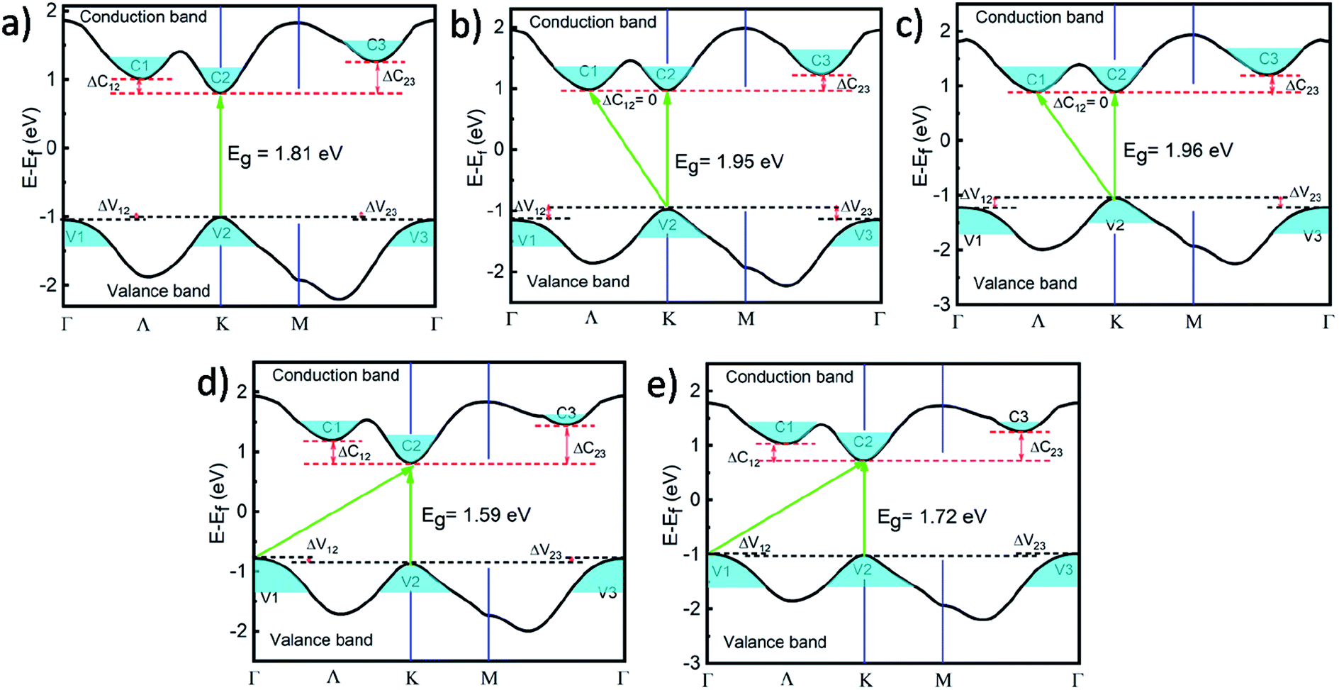
The electronic band structure of unstrained monolayer WS2 is shown in Fig. 4a. To plot the band structure we choose the k path as Γ–K–M–Γ as previous calculation.39 Our calculation shows that the highest valence band has two hole valleys at Γ point (V1 and V3) and one at K point (V2) which are almost degenerate and the energy difference between the hole valleys, ΔV12 and ΔV23 are almost zero. In the conduction band three electron valleys at K point (C2), at a point in between Γ and K point (let say Λ point) (C1) and at the point in between Γ and M (C3) and they don't show valley degeneracy as the energy difference of ΔC12 = 0.2045 eV and ΔC23 = 0.46 eV are seen in Fig. 4a. The conduction band minima (C2) and valence band maxima (V2) both lie on same K points and a direct band gap of 1.81 eV has been observed in unstrained monolayers WS2. When we apply 1% biaxial compressive strain electron valleys at K point (C2) and Λ point (C1) become degenerate as difference between these two valleys vanishes (ΔC12 = 0 eV) and ΔC23 reduces hence the conduction band shows valley degeneracy as shown in Fig. 4b. Now both direct (K–K) and indirect (K–Λ) transition can take place and both the electron valleys C1 and C2 contribute to the transport. This is why thermoelectric properties enhanced initially for n-type carries under the application of compressive strain. At the same time the hole valley at K point (V2) remains same but hole valleys at Γ point (V1 and V2) go downward and hole valley degeneracy in valence band is broken hence with the application of compressive strain thermoelectric performance of monolayer WS2 for p-type carries decreases. As we increase biaxial compressive strain the valley degeneracy in conduction band as well as valence band are broken after 2% compressive strain and the thermoelectric performances decrease (ESI Fig. S5a†). In the case of uniaxial compressive strain, the electron valley degeneracy occurs at 2% strain with a direct or indirect band gap of 1.96 eV and at this point hole valley degeneracy is broken as shown in Fig. 4c. Electron valley degeneracy disappeared slowly at higher strain and after 4% uniaxial strain degeneracy breaks (ESI Fig. S5b†).
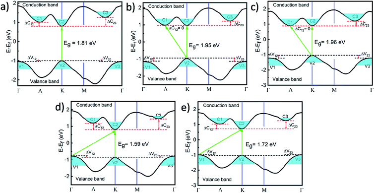 |
| | Fig. 4 Band structure and valleys of monolayer WS2 under the application of (a) 0% strain (b) −1% biaxial strain (c) −2% uniaxial strain (d) +1% biaxial strain (e) +1% uniaxial strain. Here only the highest valence band and lowest conduction band is shown. The red dotted lines and black dotted lines represent energy levels of electron valleys in conduction band and hole valleys in valence band respectively. The green arrow represents direct/indirect band gap transition between hole and electron valleys. | |
As we apply 1% tensile strain (both biaxial and uniaxial) the hole valleys V1, V2, and V3 in valence band are nearly degenerate but the difference between conduction band valleys C1, C2 and C3 increases as shown in Fig. 4d and e. As CBM lies at K point an indirect (Γ–K) or direct transition (K–K) with a band gap of 1.59 eV and 1.72 eV for biaxial and uniaxial tensile strain respectively, can take place and both hole valleys at Γ point (V1 and V3) and K point (V2) can take part in transport. This is the reason for thermoelectric power factor for the p-type doping initially increases with the application of tensile strain whereas thermoelectric properties for n-type doping decreases by tensile strain. Further enhancement of tensile strain results breaking of hole valley degeneracy very slowly (ESI Fig. S5c and d†) and the thermoelectric performances for p-type carriers also vary very slowly.
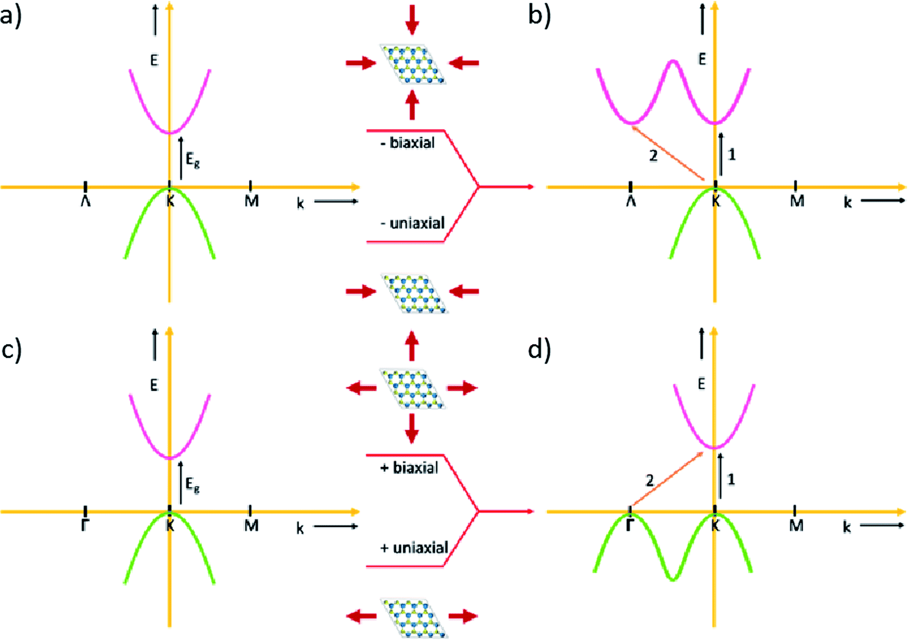
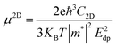
In general, the valley degeneracy in 2D materials is a phenomenon which was observed under the application of strain. The strain can be compressive or tensile in nature and can be applied in one direction or in both the directions. As shown in the schematic diagram of Fig. 5a and c, the VBM and the CBM are aligned for the unstrained WS2 and hence has a direct band gap but when a compressive strain is applied on it the transition from the valence band to the conduction band can follow multiple channels crossed as shown by paths 1 and 2 in Fig. 5b. Thus increasing the n-type carriers in the conduction band. Similarly, by the application of tensile strain the number of valleys having same energy in the valence band increases as shown in Fig. 5d, thus the number of p-type carriers in the valence band increases. So, the compressive strain and the tensile strain act in such a way that in one case it increases the number of carriers in the conduction band and in other case it increases the number of carriers in the valence band due to the valley degeneracy but limited to a lower percentage of strain. At higher strain (>4%) both the electron and hole valley degeneracy are broken because the threshold beyond which the material can't come back to the original unstrained state is crossed and as a result the thermoelectric properties decrease.
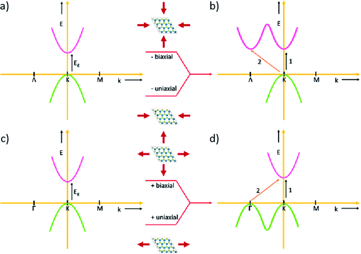 |
| | Fig. 5 Schematic representation of valley degeneracy in strained WS2. (a) Represents the E-k curve of an unstrained WS2 monolayer. (b) The same dispersion curve under compressive biaxial or uniaxial strain. (c and d) The dispersion curve under the application of tensile strain which can be either uniaxial or biaxial in nature. In figure (b) and (d) one can clearly see double valleys in the conduction band and valence band respectively. | |
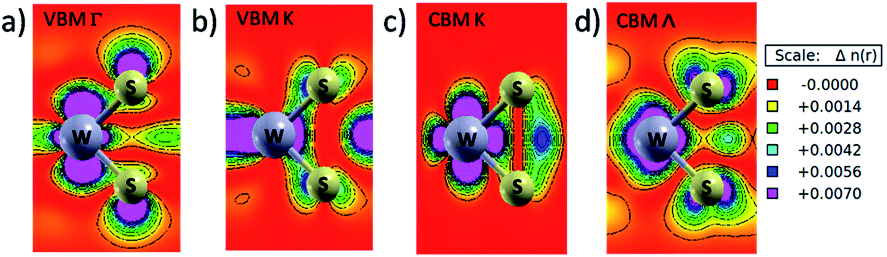
The reason for the valley degeneracy can be easily visualized from the band decomposed charge density plot shown in Fig. 6. The valence band at Γ point is mainly dominated by dz2 orbital of W atom and pz orbital of S atom whereas valence band at K point is contributed mainly by two degenerate states i.e. W atom's dx2−y2 and dxy orbitals and there is negligible contribution of S atoms at this point which is clearly seen in Fig. 6a and b. Similarly, the conduction band at K point is mainly dominated by W atom's dx2−y2 and dxy orbitals and there is very little contribution from S atoms at this point but the conduction band at Λ point (in between Γ and K points) has contribution from both W and S atoms as shown in Fig. 6c and d. So, when strain is applied the bands at K point remain relatively unchanged as bands at K point are mainly dominated by W atom which is sandwiched between two outer S atoms plane hence less sensitive to strain but the strain affects more on the two outer S atoms plane hence the VBM at Γ point and CBM at Λ point are more sensitive to applied strain and undergo valley degeneracy.
 |
| | Fig. 6 Band decomposed charge density plot of WS2. (a) The VBM at Γ point (b) the VBM at K point (c) the CBM at K point (d) the CBM at Λ point. | |
Carrier's mobility and relaxation time
The phonon limited hole and electron mobility have been calculated using the values of effective mass and deformation potential theory.40 According to this theory charge carrier mobility of 2D materials can be calculated by using the relation| |
 | (10) |
From this value of mobility, the relaxation time (τ) can be determined as τ = m*μ/e where C2D and Edp are stretching modulus and deformation potential respectively and m* = ħ2[∂2E/∂k2]−1 is the effective mass of the carriers.41 In 2D system C2D can be determined by C2D = [∂2E/∂δ2]/S0 where E, δ and S0 are total energy, amount of strain and optimized area respectively. The deformation potential (Edp) can be determined for the hole and electron by denoting the shift in VBM and CBM with respect to applied strain respectively. All the calculated parameters are summarized in Table 2. and the values are in good agreement with previous calculation for monolayer MoS2.21
Table 2 Calculated deformation potential (Edp), stretching modulus (C2D), effective mass (m*), relaxation time (τ) and mobility (μ2D) of electron and hole in monolayer WS2
| |
Edp (eV) |
C2D (N m−1) |
m* |
τ (fs) |
μ2D (cm2 V−1 s−1) |
| Electron |
14.00 |
164.097 |
0.3500 |
19.40 |
97.33 |
| Hole |
6.582 |
164.097 |
0.5125 |
59.92 |
205.36 |
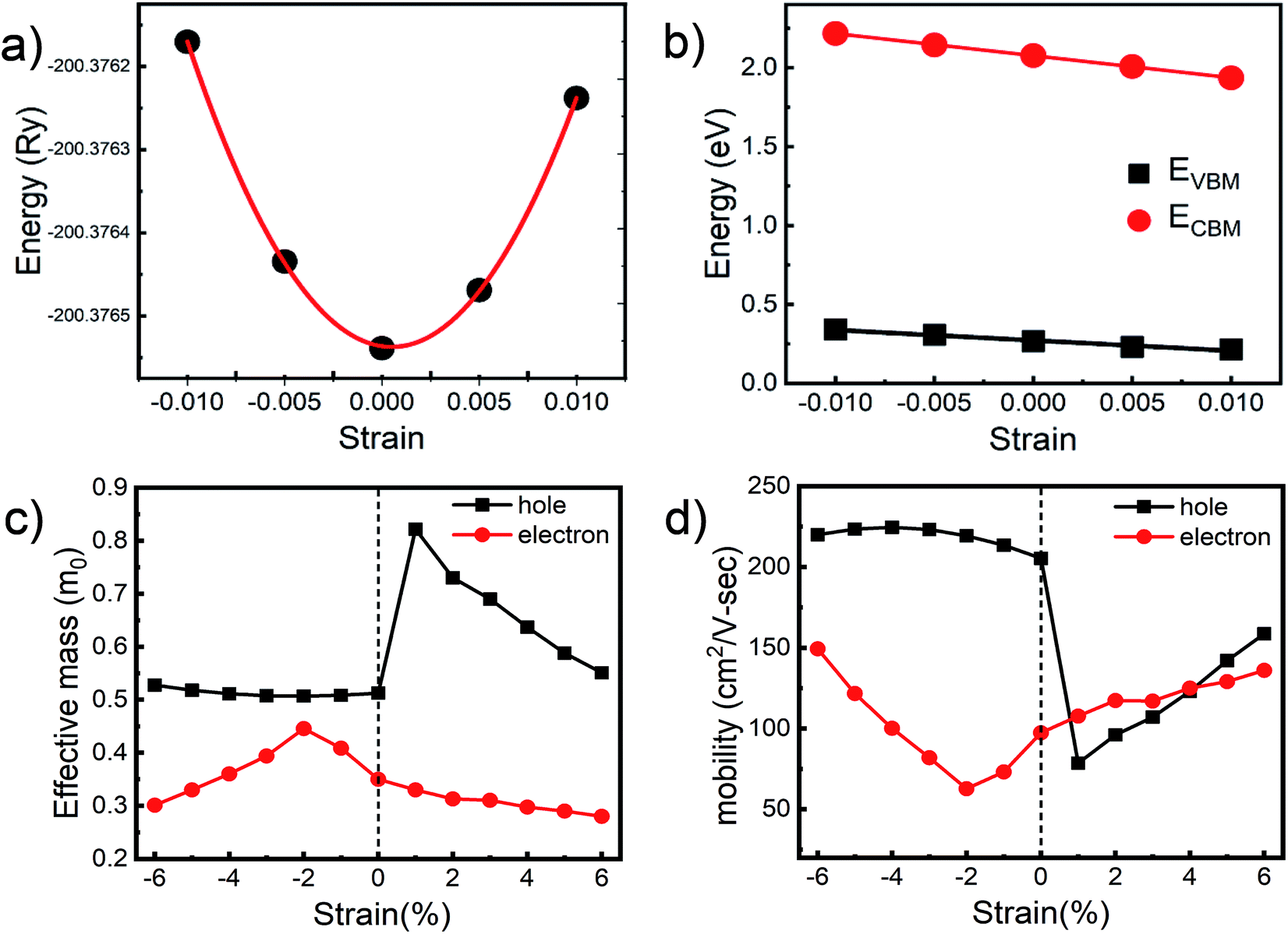
The variation of effective mass and carrier mobility with application of biaxial strain is shown in Fig. 7c and d. The effective mass and mobility do not vary much for hole as compared to that of electron with applied compressive strain but for electron there is significant change implies that compressive strain is more effective for n-type carriers. There is a sharp fluctuation at 2% compressive strain for electron because of the shifting of CBM from high symmetry K point to a point in between Γ and K point resulting a direct to indirect band gap transition at this point. As tensile strain is applied the effective mass and mobility does not vary significantly for electron but significant changes are observed for hole indicates that tensile strain is more effective for p-type carriers. Here also a very sharp fluctuation is observed at 1% of tensile strain for hole due to the shifting of VBM from high symmetry K point to Γ point results a direct to indirect band gap transition at this point. So, these fluctuations are the indication of shifting of VBM and CBM resulting direct to indirect band gap transition. When the mobility of a nanoribbon of 2D materials is calculated, the values of mobility are different for zigzag and arm chair directions.42,43 So, we have also calculated the directional mobility of WS2, but as we have considered only the 2 × 2 super cell for the calculation, the variation in the carrier mobility for electrons is not appreciable except in the biaxial strain where it has increased three times that of due to uniaxial strain.
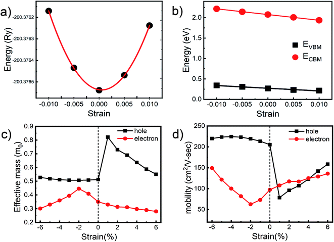 |
| | Fig. 7 The variation of (a) total energy with applied strain and (b) shift in the VBM and CBM with applied strain to determine deformation potential and variation in (c) effective mass and (d) carrier mobility as a function of biaxial strain at room temperature. | |
Conclusions
In conclusion, we have performed strain dependent studies of electronic and thermoelectric properties of monolayer WS2 by using DFT and Boltzmann transport theory. We have calculated thermoelectric properties as a function of chemical potential and carrier concentration and found that both the approaches give same output. The enhancement of the thermoelectric performances has been found with the application of compressive strain for n-type doping and that of tensile strain for p-type doping. Among all types of strains uniaxial compressive strain has been found to be most effective and highest thermoelectric PF and ZT product have been found to be 59 × 1010 W m−1 K−2 s−1 and 0.72 respectively at 900 K under 4% of uniaxial compressive strain. The enhancement of thermoelectric properties is due to the degeneracy of bands near the Fermi level and can be confirmed from the band decomposed charge density contours. These results clearly indicate that WS2 could be a very promising material for thermoelectric applications under applied compressive strain.
Conflicts of interest
There are no conflicts to declare.
Acknowledgements
The authors are thankful to Ministry of Human Resource and Development (MHRD) India for supporting this work. We are also thankful to Indian Institute of Technology Jodhpur (IITJ) for all the supports to carry out the experiment.
References
- G. R. Bhimanapati, Z. Lin, V. Meunier, Y. Jung, J. Cha, S. Das, D. Xiao, Y. Son, M. S. Strano, V. R. Cooper, L. Liang, S. G. Louie, E. Ringe, W. Zhou, S. S. Kim, R. R. Naik, B. G. Sumpter, H. Terrones, F. Xia, Y. Wang, J. Zhu, D. Akinwande, N. Alem, J. A. Schuller, R. E. Schaak, M. Terrones and J. A. Robinson, ACS Nano, 2015, 9, 11509–11539 CrossRef CAS PubMed.
- Q. H. Wang, K. Kalantar-Zadeh, A. Kis, J. N. Coleman and M. S. Strano, Nat. Nanotechnol., 2012, 7, 699 CrossRef CAS PubMed.
- W. Huang, H. Da and G. Liang, J. Appl. Phys., 2013, 113, 104304 CrossRef.
- H. Osterhage, J. Gooth, B. Hamdou, P. Gwozdz, R. Zierold and K. Nielsch, Appl. Phys. Lett., 2014, 105, 123117 CrossRef.
- Y. Cai, H. Zhou, G. Zhang and Y.-W. Zhang, Chem. Mater., 2016, 28, 8611–8621 CrossRef CAS.
- S. Bhattacharyya, T. Pandey and A. K. Singh, Nanotechnology, 2014, 25, 465701 CrossRef PubMed.
- Z. Ding, Q.-X. Pei, J.-W. Jiang and Y.-W. Zhang, J. Phys. Chem. C, 2015, 119, 16358–16365 CrossRef CAS.
- Y. Gong, J. Lin, X. Wang, G. Shi, S. Lei, Z. Lin, X. Zou, G. Ye, R. Vajtai, B. I. Yakobson, H. Terrones, M. Terrones, B. K. Tay, J. Lou, S. T. Pantelides, Z. Liu, W. Zhou and P. M. Ajayan, Nat. Mater., 2014, 13, 1135 CrossRef CAS PubMed.
- D. Wickramaratne, F. Zahid and R. K. Lake, J. Chem. Phys., 2014, 140, 124710 CrossRef PubMed.
- J. Pu, K. Kanahashi, N. T. Cuong, C.-H. Chen, L.-J. Li, S. Okada, H. Ohta and T. Takenobu, Phys. Rev. B, 2016, 94, 014312 CrossRef.
- A. A. Ramanathan and J. M. Khalifeh, IEEE Trans. Nanotechnol., 2018, 17, 974–978 CAS.
- C. Lee, J. Hong, M. H. Whangbo and J. H. Shim, Chem. Mater., 2013, 25, 3745–3752 CrossRef CAS.
- C. Lee, J. Hong, W. R. Lee, D. Y. Kim and J. H. Shim, J. Solid State Chem., 2014, 211, 113–119 CrossRef CAS.
- J. Su, Z. T. Liu, L. P. Feng and N. Li, J. Alloys Compd., 2015, 622, 777–782 CrossRef CAS.
- X. Liu, G. Zhang, Q. X. Pei and Y. W. Zhang, Appl. Phys. Lett., 2013, 103, 1–6 Search PubMed.
- K. Hippalgaonkar, Y. Wang, Y. Ye, D. Y. Qiu, H. Zhu, Y. Wang, J. Moore, S. G. Louie and X. Zhang, Phys. Rev. B, 2017, 95, 115407 CrossRef.
- M. Buscema, M. Barkelid, V. Zwiller, H. S. J. Van Der Zant, G. A. Steele and A. Castellanos-Gomez, Nano Lett., 2013, 13, 358–363 CrossRef CAS PubMed.
- J. Hong, C. Lee, J.-S. Park and J. H. Shim, Phys. Rev. B, 2016, 93, 35445 CrossRef.
- S. Ahmad and S. Mukherjee, Graphene, 2014, 03, 52–59 CrossRef.
- B. Amin, T. P. Kaloni and U. Schwingenschlögl, RSC Adv., 2014, 4, 34561–34565 RSC.
- H. V. Phuc, N. N. Hieu, B. D. Hoi, N. V. Hieu, T. V. Thu, N. M. Hung, V. V. Ilyasov, N. A. Poklonski and C. V. Nguyen, J. Electron. Mater., 2018, 47, 730–736 CrossRef CAS.
- S. Bhattacharyya and A. K. Singh, Phys. Rev. B: Condens. Matter Mater. Phys., 2012, 86, 1–7 Search PubMed.
- W. Shen, D. Zou, G. Nie and Y. Xu, Chin. Phys. B, 2017, 26, 117202 CrossRef.
- H. Soni and P. K. Jha, AIP Adv., 2015, 5, 1–7 Search PubMed.
- Dimple, N. Jena and A. De Sarkar, J. Phys. Condens. Matter, 2017, 29, 225501 CrossRef CAS PubMed.
- L. Zhu, T. Zhang, Z. Sun, J. Li, G. Chen and S. A. Yang, Nanotechnology, 2015, 26, 465707 CrossRef PubMed.
- D. Zou, S. Xie, Y. Liu, J. Lin and J. Li, J. Mater. Chem. A, 2013, 1, 8888–8896 RSC.
- R. Tan, C. Zou, K. Pan, D. Zou and Y. Liu, J. Alloys Compd., 2018, 743, 610–617 CrossRef CAS.
- P. E. Blöchl, Phys. Rev. B, 1994, 50, 17953 CrossRef PubMed.
- J. P. Perdew, Phys. Rev. Lett., 1997, 78, 1396 CrossRef CAS.
- J. P. Perdew, K. Burke and M. Ernzerhof, Phys. Rev. Lett., 1996, 77, 3865 CrossRef CAS PubMed.
- P. Giannozzi, S. Baroni, N. Bonini, M. Calandra, R. Car, C. Cavazzoni, D. Ceresoli, G. L. Chiarotti, M. Cococcioni and I. Dabo, J. Phys.: Condens. Matter, 2009, 21, 395502 CrossRef PubMed.
- G. K. H. Madsen and D. J. Singh, Comput. Phys. Commun., 2006, 175, 67–71 CrossRef CAS.
- A. Togo, L. Chaput and I. Tanaka, Phys. Rev. B: Condens. Matter Mater. Phys., 2015, 91, 94306 CrossRef.
- Z. Y. Zhu, Y. C. Cheng and U. Schwingenschlögl, Phys. Rev. B, 2011, 84, 153402 CrossRef.
- T. C. Berkelbach, M. S. Hybertsen and D. R. Reichman, Phys. Rev. B: Condens. Matter Mater. Phys., 2013, 88, 45318 CrossRef.
- T. Li, C. He and W. Zhang, J. Mater. Chem. A, 2019, 7, 4134–4144 RSC.
- H. J. Goldsmid and J. W. Sharp, J. Electron. Mater., 1999, 28, 869–872 CrossRef CAS.
- C. He, J. H. Zhang, W. X. Zhang and T. T. Li, J. Phys. Chem. Lett., 2019, 10, 3122–3128 CrossRef CAS PubMed.
- J. Bardeen and W. Shockley, Phys. Rev., 1950, 80, 72 CrossRef CAS.
- M. M. Dong, C. He and W. X. Zhang, J. Mater. Chem. C, 2017, 5, 3830–3837 RSC.
- M.-Q. Long, L. Tang, D. Wang, L. Wang and Z. Shuai, J. Am. Chem. Soc., 2009, 131, 17728–17729 CrossRef CAS PubMed.
- T. T. Li, C. He and W. X. Zhang, Appl. Surf. Sci., 2018, 441, 77–84 CrossRef CAS.
Footnote |
| † Electronic supplementary information (ESI) available. See DOI: 10.1039/c9ra04470a |
|
| This journal is © The Royal Society of Chemistry 2019 |
Click here to see how this site uses Cookies. View our privacy policy here. 
 Open Access Article
 This Open Access Article is licensed under a Creative Commons Attribution-Non Commercial 3.0 Unported Licence
 *
*
 where a0 and a are the lattice constant of relaxed and strained structures respectively. For the thermoelectric and transport properties, a semi classical Boltzmann transport theory was used with constant scattering time approximation (CSTA) as implemented in BoltzTrap33 code. In CSTA we assume that scattering time has very less dependency on energy and both the group velocity of carriers and DOS contribute to the transport function. The group velocity (vg) of carriers in a specific band can be described as
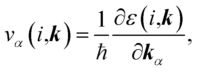

 is the Fermi–Dirac distribution function.