
 Open Access Article
 This Open Access Article is licensed under a Creative Commons Attribution-Non Commercial 3.0 Unported Licence
Capillary liquid bridge soft lithography for micro-patterning preparation based on SU-8 photoresist templates with special wettability†
Huijie Wang *a,
Xiaoxun Lib,
Kang Luanb and
Xilin Baia
*a,
Xiaoxun Lib,
Kang Luanb and
Xilin Baia
aMultiscale Frontier Physics Research Center, School of Physics and Information Engineering, Shanxi Normal University, Linfen, 041004, P. R. China. E-mail: wanghj@sxnu.edu.cn
bKey Laboratory for Special Functional Materials of Ministry of Education, Collaborative Innovation Center of Nano Functional Materials and Applications, Henan University, Kaifeng 475004, P. R. China
First published on 2nd August 2019
Abstract
Patterned micro-nano arrays have shown great potential in the fields of optics, electronics and optoelectronics. In this study, a strategy of interface-induced dewetting assembly based on capillary liquid bridges and SU-8 photoresist templates is proposed for patterning organic molecules and nanoparticles. First, photoresist templates with chemical stability were prepared via a simplified lithography method. Then the interface wettability and the contact angle hysteresis of water droplets on the fluorosilane modified templates were adequately studied and discussed. Subsequently, a sandwich structure, composed of a superhydrophilic target substrate, a hydrophobic high adhesive photoresist template and a growth solution were introduced for the confined space dewetting assembly. The related mechanism was investigated and revealed, with the assistance of in situ observation via a fluorescence microscope. Finally, the patterned arrays of water-soluble organic small molecules and aqueous dispersed nanoparticles were successfully obtained on the target substrates. This method is simple and easy, and the SU-8 photoresist templates possess a series of advantages such as low processing cost, short preparation periods and reusable performance, which endow this strategy with potential for application in molecular functional devices.
1 Introduction
Patterned functional materials offer substantial potential for constructing photo-electric devices, such as transparent conductive films, light-emitting diodes, photodetectors, optical waveguides and wearable sensors,1–6 etc. A series of preparation techniques have been developed, including photolithography, electron beam etching, ion beam etching and laser processing. However, some deficiencies still exist such as high cost output, precise instrument requirements, and long-time fine manipulation. To overcome these disadvantages, George Whitesides et al. proposed and developed soft lithography technology combining microcontact printing and micromold soft printing techniques. In their methods, the fabrication of patterned functional materials mainly depends on the preparation of soft templates such as PDMS molds, the selective interface modification of self-assembled monolayer molecules such as alkyl hydrosulfide, and the relevant chemical reactions.7–9 High-quality patterns and structures can be produced via this technology and are applied in the biological and photoelectric fields.10–12 However, the popularization of soft lithography is still limited on account of the disadvantages of large elasticity and easy swelling of PDMS materials, and the tedious experimental procedures. In recent years, Si templates with three-dimensional micro-topographies (such as pillars or spindles) are gradually arousing researchers' interests in patterned nanoparticle self-assembly or crystal growth via liquid bridges between the template and the target substrate.13,14 In order to build liquid bridges, the templates are commonly designed as an asymmetric wetting structure between the top and side walls for liquid pinning.15 Based on the patterning arrays, integrated sensors, laser devices and photodetectors can be fabricated.15–17 What limits their practicality are high power consumption during the plasma etching process of the silicon pillar template, the toxicity of fluorine-containing gas, and the fragility of the Si template microstructures. Besides, constructing a two-dimensional hydrophilic–hydrophobic micro-patterned template is also a candidate strategy for patterning functional materials, which can greatly improve the selective wetting of liquids on the surface of substrates. The common preparation approaches include selective irradiation using ultraviolet light, thermal treatment, pH regulation and other external stimuli.18–20 Though it presents some advantages in the aspects of controlling the droplet geometry, effectively locating the droplet and accurately distributing the aqueous solution to the hydrophilic zone,21,22 the disadvantages are obvious from their complicated fabrication processes and the non-reusable templates.For the last two decades, the SU-8 photoresist materials have been developed and widely used in electronic industries such as microfluidic control, microelectronics machining and chip packaging,23–25 which is mainly attributed to their unique features including their good light transmittance, mechanical property, chemical stability, thermal resistance and biological compatibility. An outstanding advantage is that the micro-configurations with high aspect ratio are easily obtained via simple lithography.26,27 From a comprehensive perspective, the SU-8 photoresist templates may be good alternatives to PDMS templates, silicon templates and the two-dimensional templates with composite wettability in interface lithography.
Moreover, conventional lithography exploits poorly chemically stable positive photoresist such as SPR220 or negative adhesive such as an acrylic resin-containing photoresist to facilitate later photoresist removal, but it introduces some unfavourable factors, for example, the photoresist pattern line edges are not smooth enough, and the chemical agents or gases introduced in the photoresist development or removal process will corrode the organic or biological target materials.28,29 Compared to conventional photoresist-based lithography, SU-8 photoresist based on interface printing technology undoubtedly also owns broad application prospects. Deng and Jie et al. prepared several kinds of organic molecular arrays via the one-dimensional directional induction of photoresist templates, and assembled them to electric devices.30–33 However, it faces a remarkable problem that the templates could not be reused because the functional molecules and the stable photoresist templates are grown together; meanwhile, the coexisting template also reduces the performance of molecular devices to some extent.
In this study, SU-8 photoresist templates with good hydrophobicity and high adhesion are prepared for interface lithography. The surface wettability of photoresist templates is systematically studied. By making use of the asymmetric wettability between the photoresist template and the superhydrophilic substrate, capillary liquid bridges are generated in the confined space, and the organic small molecules and the nanoparticles are further patterned on the superhydrophilic substrate. The dewetting mechanism during the assembly process is investigated with the assistance of in situ observation via a fluorescent microscope. Our strategy presents many advantages over previous work: first, it simplifies the tedious experimental procedures compared with preparing hydrophilic–hydrophobic patterned templates. Second, it greatly saves the cost compared with the Si template. Furthermore, the template can be reused after cleaning for the reason that the arrays can directly be assembled on the substrate. This study enriches the content of soft lithography, provides an experimental basis for the application of patterned SU-8 photoresist materials to the fields of molecular patterning, nanoparticle assembly and device integration.
2 Experiment
2.1 Materials and reagents
The silicon wafer and glass were obtained from the market, SU-8 2015 photoresist and its developer were bought from Microlithography Chemical Corporation of the United States. The organic small molecule Rhodamine B (AR) was purchased from Shanghai Sinopharm Chemical Reagent Co., Ltd. The CdSe quantum dots were synthesized in the laboratory and dispersed in water. Fluorosilane (CF3(CF2)7(CH2)2Si(OCH3)3, FAS) was purchased from Dow Corning (the molecular structure depicts in Fig. S1a†) of the United States. The glass slides, silicon wafer, and Si/SiO2 (300 nm SiO2 oxide layer) substrate were bought from the market. Deionized water (resistivity 18.25 Ω cm) acted as the molecular solvent and nanoparticle dispersant.2.2 Sample preparation
Surface cleaning. The polished surface of silicon wafer was cleaned using a standard RCA method.34 The glass slides and Si/SiO2 substrate were successively ultrasonically cleaned in acetone, ethanol and deionized water for 10 min, respectively, and then dried under nitrogen.
SU-8 photoresist template preparation. The detail is offered in Fig. 1. First, the photoresist was spin-coated on the polished surface of Si substrate at a speed of 4000 rpm for 60 s. Then the sample was prebaked on a 95 °C heating stage for 2 min. Second, photolithography of the SU-8 photoresist film was performed using a mask aligner, and the sample was exposed under UV irradiation (the irradiance density is 15 mW cm−2) for 8 s through a photo-mask plate. After being post-baked at 95 °C for 3 min, the sample was developed in the developer for 60 s and rinsed in water for 5 s to form the photoresist patterns. Finally, the patterned SU-8 photoresist was directly exposed under UV irradiation for another 10 min for the full molecular crosslinking. The final sample acted as the SU-8 photoresist template. Considering the limitations of the processing technology, the photoresist strips we prepared are segmented structures. The cost for the SU-8 photoresist templates prepared on a 4 inch wafer is about 500 CNY, far below the cost of Si template (more than 2000 CNY) according to the current market.
 | ||
| Fig. 1 Schematic diagram of SU-8 photoresist template preparation. | ||
Preparation of photoresist planar film. The planar film of photoresist was obtained by directly spin coating, baking and exposure process. The details are offered in the ESI.†
Low surface energy modification. FAS was introduced to lower the surface energy of photoresist template via a thermal evaporation process.35 In short, the template and 50 μL of FAS were sealed together in a glass container, before being heated in a drying oven at 90 °C for 3 h (see Fig. S1b†).
Interface-induced dewetting assembly based on the SU-8 photoresist templates. A schematic diagram is shown in Fig. S2.† Firstly, the small molecule aqueous solution was prepared by dissolving the Rhodamine B powder into deionized water at room temperature, and nanoparticle aqueous dispersion was also prepared by dispersing the nanoparticles into deionized water. Secondly, 10 μL of liquid was dropped on the surface of the photoresist template using a micro-injector. Lastly, a superhydrophilic target substrate was rapidly covered on the surface (the cleaned substrate was treated with O2 plasma for 3 min to be superhydrophilic) to form a sandwich structure. Subsequently, the sample was transferred into a 60 °C drying oven. After 1 h reaction, the sample was taken out, and the target substrate and the photoresist template were separated at room temperature.
2.3 Characterizations
The static contact angle (CA), advancing contact angle (AA) and receding contact angle (RA) were measured via an optical video contact angle measuring instrument (OCA20, DataPhysics, Germany). The volume of the individual water droplet in all tests was 5 μL, and the average CA values were obtained by measuring the same sample on at least five different positions. The measurement error is controlled within 1°. Fluorescence confocal microscope system with CCD lens (FV-1000, Olympus, Japan) was used for the observation of optical and fluorescent images. The microscopic morphological images were characterized by scanning electron microscope (SEM, JSM-7500F, Japan electron, Japan), atomic force microscope (AFM, OLS4500, Olympus, Japan) and transmission electron microscopy (TEM, JEM2100, JEOL, Japan). Crystallization analysis was carried out via an X-ray diffractometer (Empyrean type, PANalytical B.V., the Netherlands).3 Results and discussion
3.1 The morphology characterization of the photoresist template
Scanning electron microscope (SEM) was used to observe the photoresist configuration, as shown in Fig. 2. It can be seen from the top view (Fig. 2a) and side view (Fig. 2b) that the photoresist template owns a uniform pillar array structure; and the surface of the photoresist micro-pillars is smooth, without obvious defects. In an enlarged side view (Fig. 2c), the average height of the micro-pillars is measured as 12 μm, and the average width of the bottom of the micro-pillars is 5 μm, which is consistent with the pre-set size on the lithographic mask. The average top width is 5.6 μm, slightly wider than the bottom, which originates from the over-exposure because of the diffraction effect of the mask plate. The photoresist pillar structure is relatively steep (the angle between the surface and the side is 88° according to a calculation), which is conducive to the induced assembly at the later stage. For a planar photoresist film, the surface is also very smooth in a large area (more than 300 μm × 300 μm), see Fig. S3b.† | ||
| Fig. 2 The SEM images of SU-8 photoresist template. (a) Top view; (b) side view; and (c) enlarged side-view. | ||
3.2 The wettability of the water droplet on the SU-8 photoresist template
The CA of a water droplet on photoresist planer film and photoresist templates were measured. The results are shown in Fig. S3† and 3. From Fig. S3,† the intrinsic CA for water droplet on photoresist planar film is 85.0° (see Fig. S3a†). After being modified by FAS, the CA turns to 114.0° (see Fig. S3c†), demonstrating the planar film achieves an obvious hydrophobic property. | ||
| Fig. 3 The anisotropic wettability of water droplet on a SU-8 photoresist template (sample 5-10-200-50). (a) The schematic diagram of photoresist template parameters and contact angle observation directions; (b) the CA observed from different directions. | ||
The photoresist template sample with 5 μm bottom width (a1), 10 μm transverse space (b1), 200 μm pillar length (a2), and 50 μm longitudinal space (b2) is defined as 5-10-200-50 (a1-b1-a2-b2). A graphical description of the parameters is presented in Fig. 3a, and the optical image of the template 5-10-200-50 is offered in Fig. S4.† This definition is appropriate for other samples as well. The CAs of FAS modified photoresist templates were measured from two observed directions, along with the pillars and perpendicular to the pillars, respectively (see Fig. 3a), and the test results of CAs are shown in Table S1.†
For the sample 5-10-200-50, the CA observed along with the pillars is 137.0°, and the CA measured perpendicular to the pillars is 121.0° (Fig. 3b). The optical image of the test water droplet is shown in the inset in Fig. S4,† and a slight stretch of the droplet can be found along with the pillars. It can be seen the obvious anisotropic wettability exists owing to the asymmetry of three-phase contact line in different directions. For the templates 5-10-100-25 and 5-10-500-50, there also exist significant differences (more than 15.0°) for the CA values observed from the two mutually orthogonal directions, see Table S1.† The related analysis is offered in ESI.† The results indicate that the droplets can spread more easily along the column direction with regard to our templates with pillar structures, see the droplet in Fig. 3c.
For a square columns template (5-10-5-10), the corresponding two CAs are 140.0° and 139.5°, the approximate values originate from the symmetry of triple-phase contact line (TCL) in the crossed directions.
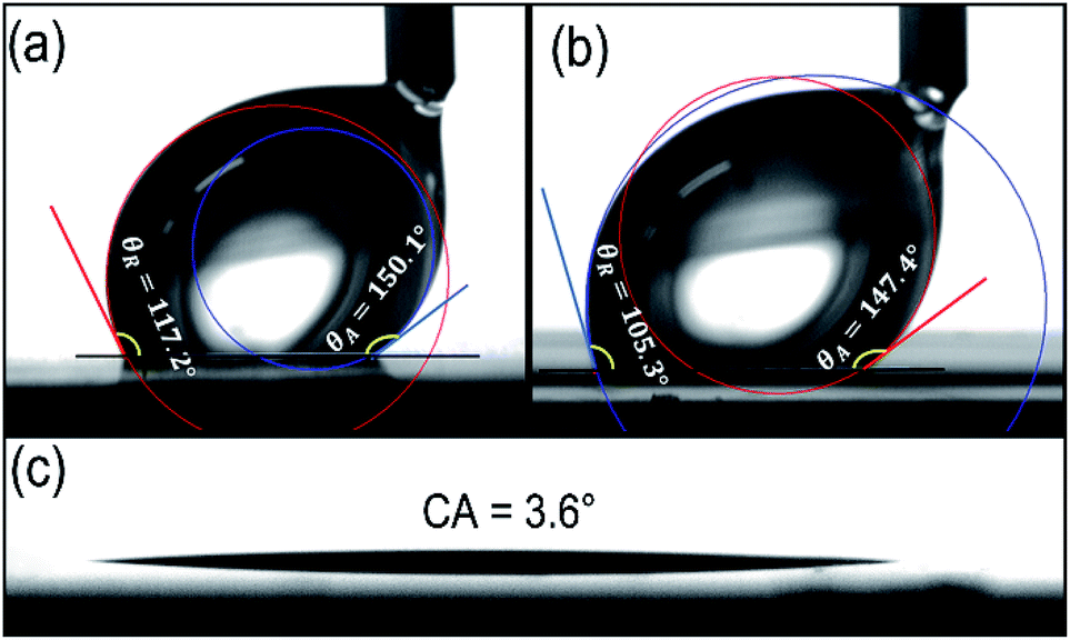
Generally, the solid surface with good hydrophobicity and high adhesion demonstrates obvious advantages in clinging and transferring water droplets. And microfluidic bridges can form between the three-dimensional microarray structures and a hydrophilic substrate to induce the crystal growth of solution.13 For the FAS modified photoresist template (5-10-200-50) in this study, the AA (θA) and RA (θR) were measured via a tip dragging method,36 while the dragging direction was orthogonal to the viewing direction, see Fig. S5.† The CAH is the absolute value of the difference between AA and RA. The results are depicted in Fig. 4a and b. In the observed direction along with the pillars, the CAH value is 32.9°, and in the observed direction perpendicular to the pillars, the CAH value is 42.1°, which demonstrate a high adhesion of the template surface to water droplets.
 | ||
| Fig. 4 The contact angle hysteresis of water droplet on the SU-8 photoresist template (5-10-200-50) and the wettability of water droplet on the target substrate. (a) Observation along with the pillars; (b) observation perpendicular to the pillars; and (c) the wettability for the plasma treated target substrate. | ||
The CAH for other photoresist templates are also measured, and the results are offered in Table 1. The CAH values for all templates present a difference in the two orthogonal directions, but there are no obvious change rules to follow. On the whole, all the templates show high adhesion to water droplet.
| Sample (a1-b1-a2-b2) | Observation along with the pillars | Observation perpendicular to the pillars |
|---|---|---|
| 5-10-5-10 | 28.0° | 28.5° |
| 5-10-100-25 | 34.2° | 40.0° |
| 5-10-200-50 | 32.9° | 42.1° |
| 5-10-500-50 | 36.0° | >45.0° |
The high adhesive and high hydrophobic template with pillar arrays contributes to the pinning and induction of liquid in a confined space. The target substrate was chosen as hydrophilic glass or Si/SiO2 substrate (with 300 nm SiO2 oxide layer), the water contact angle are shown in Fig. S6.† Before being used, the surface was treated with O2 plasma (200 W) for 3 min to realize its surface superhydrophilicity (see Fig. 4c), which benefits the liquid adsorption. The asymmetric liquid bridges can generate between a superhydrophilic substrate and a hydrophobic high adhesive template, as depicted in the schematic diagram of Fig. S7.†
3.3 The stability tests
 | ||
| Fig. 5 The optical image and water contact angle for photoresist template before and after being soaked in toluene. (a) Before being soaked; and (b) after being soaked. | ||
3.4 The mechanism analysis of interface-induced dewetting assembly based on the photoresist template with special wettability
The patterned organic small molecules and nanoparticles were prepared via a sandwich method. The patterned printings were realized on the basis of the asymmetric interface wettability between the photoresist templates (with good hydrophobicity and high adhesion) and the target substrates (with superhydrophilicity). In the beginning, a stable ellipsoid crown is formed after a water droplet is dropped on the surface of the template, on account of the interface pinning effect and the tension balance on the three-phase contact line. Then a target substrate is overlaid on the template, and the droplet is squeezed and spread out over the entire surface, as shown in Fig. 6a. Because of the good hydrophobicity of the template, a gas film will form under the liquid film between the adjacent pillars. With the evaporation of the aqueous solution, the dewetting process of liquid film begins. Under the synergistic effect of the pillars induction, the air pressure and the Laplace pressure, the rapture of liquid film happens, generating isolated micro-scaled capillary bridges anchored onto the micro-pillars of the photoresist template, as shown in Fig. 6b. The liquid bridges shrink till they break, and a regular one-dimensional molecular array can form on the desired target substrate after the complete liquid evaporation, as shown in Fig. 6c. Due to the huge difference of the wettability between the hydrophobic-high adhesive photoresist pillars and the superhydrophilic substrate, the molecular arrays will mainly be generated on the substrate. | ||
| Fig. 6 The investigation of the dewetting mechanism during the interface-induced dewetting assembly of molecular array. (a)–(c) Diagram of the assembly process; (d)–(f) the optical images of in situ observation at different reaction time; and (e1)–(e3) the mechanism diagrams of the dewetting process at different stages corresponding to the zone 1–3 in (e) respectively. | ||
In order to elucidate the assembly process more intuitively, the in situ observation via a fluorescence microscope was performed. In the experiment, a drop of Rhodamine B solution with a concentration of 8 mg mL−1 is confined between a photoresist template and a target substrate. The optical images at different time are depicted in Fig. 6d–f. At the first minute, the liquid rapidly wets the entire interface under the external pressure, forming a liquid film. Meanwhile, the pillars are faintly visible, as shown in Fig. 6d. The result is corresponding to Fig. 6a. Then, under the action of the liquid evaporation, the liquid film rapidly cracks in the direction perpendicular to pillars because of the wide space intervals, as shown in the blue part above the pillars in Fig. 6e. Subsequently, at the 30th minute, the liquid film above the air columns between the adjacent paralleled pillars are broken with the dewetting process progresses, as depicted in Fig. 6e. Finally, at the 60th minute, fluorescent molecular arrays are formed, see Fig. 6f, which is in accordance with Fig. 6c.
Based on the different liquid states in three zones (1–3) in Fig. 6e, the mechanism of the dewetting process is revealed. In zone 1, the liquid film between the mutually parallel pillars starts to retreat, corresponding to the shrinkage of the liquid film toward the substrate driven by the water evaporation, as shown in Fig. 6e1. In zone 2, the liquid film breaks between the parallel pillars, corresponding to that liquid bridge arrays formed following the liquid film shrinks and fractures toward the substrate, see Fig. 6e2. In zone 3, the liquid above the column shrinks and darkens, corresponding to the shrinkage of the liquid bridge until it cracks, as shown in Fig. 6e3.
3.5 Characterization of patterned arrays through the interface-induced dewetting assembly
The Rhodamine B molecule arrays generated on glass are characterized, whose interface assembly is induced by the photoresist template 5-10-200-50 (the corresponding solution concentration is 8 mg mL−1). The results are shown in Fig. 7. In the optical image, Rhodamine B molecule arrays with a length larger than 100 μm are obtained through the interface induced assembly (Fig. 7a); meanwhile, the Rhodamine B molecular arrays own good fluorescence characteristic (Fig. 7b). As depicted in the SEM image, the 4 μm width micro-wire possesses a flat and smooth surface (Fig. 7c). The side view for the micron wire arrays is shown in Fig. S10,† and the height for the micron wires is measured as 580 nm according to the cross-section image of single wire. To test the surface roughness, the microwires (not the same wires) were characterized by AFM (Fig. S11†). It presents a trapezoidal section, which arises from the dewetting process (Fig. S11b†). It also demonstrates a low root mean square roughness of Rq = 0.578 nm (for a 1.0 × 1.0 μm2 area) (Fig. S11c†), which verifies the smooth of the top of the microwire. The defects appearing in Fig. 7 may originate from many factors, such as the irregular dewetting process, the uneven liquid concentration distribution on the surface, and even the inevitable defects of the photoresist template. To make the XRD test, the Rhodamine B molecular arrays are grown on a superhydrophilic single crystal silicon wafer. The Rhodamine B powder was directly tested on a frosted glass substrate in the XRD instrument. In the X-ray diffraction spectrum, the micro-wire arrays only have two distinct diffraction peaks, as indicated in the dashed oval frame in Fig. 7d, compared to the multimodality of Rhodamine B powder. This reflects a good molecular arrangement in the one-dimensional crystal array structure (the crystal face information Rhodamine B cannot be detected in the crystallization database and related literature, so it is not marked). | ||
| Fig. 7 Characterization of the generated Rhodamine B small molecule array. (a) Optical image; (b) fluorescent image; (c) SEM image; and (d) the XRD spectrum. | ||
As the concentration of Rhodamine B solution is set as 4 mg mL−1 and 12 mg mL−1, the regular molecular arrays are also generated through the template-induced method, see Fig. S12.† According to this optical images, the average widths of the resultant micro-wires are 3.5 μm and 6 μm, respectively. It presents a positive but non-linear relationship between the micro-wires width and the solution concentration, and a practicality of this method in the field of molecule patterning.
It is worth noting that the template owns good reusability, and it can be reused at least five times according to the contact angle (along with the pillars) monitoring (see Fig. S13†).
The method is also appropriate for water dispersive nanoparticles. The fluorescent quantum dots can be integrated into the optical display devices such as LED because of its good optical and quantum properties.3 In this study, CdSe quantum dots are dispersed in water to form a 10 mg mL−1 dispersion. It can be measured according to the TEM image (the inset in Fig. 8a) that the average diameter of the prefabricated quantum dots is 10 nm; the small size of quantum dots contributes to their uniform dispersion in liquid. Then the template-induced assemblies are conducted using different SU-8 photoresist templates. The resultant fluorescent images of CdSe quantum dot arrays are shown in Fig. 8. Fig. 8a shows a one-dimensional assembled array induced by the photoresist template 5-10-200-50. Fig. 8b depicts a zero-dimensional quantum dot arrays induced by a square pillar photoresist template 5-10-5-10. In conclusion, the patterned assembly of nanoparticles is successfully realized through the induction of photoresist templates, which endows this approach with potential for application to micro-nano functional devices.
 | ||
| Fig. 8 The fluorescent images of assembled CdSe quantum dots using the photoresist template-induced method. (a) One-dimensional quantum dot array, the inset is the TEM image of the quantum dots; and (b) zero dimensional quantum dot arrays. | ||
4. Conclusions
In this paper, we proposed a soft lithography strategy based on capillary bridge and SU-8 photoresist template with special wettability, which is dedicated to patterning the molecules and nanoparticles through an interface-induced dewetting assembly process. Firstly, a simplified lithography technique was developed to prepare a SU-8 photoresist template with chemical stability and high aspect ratio. Secondly, the anisotropic wettability and the high adhesion of the hydrophobic templates was analysed and discussed. Subsequently, taking advantage of the asymmetric wettability between the superhydrophilic target substrate and the photoresist template, a sandwich reaction structure capable of generating liquid bridges was introduced for the molecular patterning. Finally, the patterned arrays of organic small molecule and nanoparticles were successfully assembled on the target substrates. Moreover, an in situ observation via a fluorescent microscope provides us with an insight into the dewetting process and the mechanism of molecular patterned array. This strategy presents many advantages over previous work: simple steps comparing with fabricating a hydrophilic-hydrophobic patterned substrate;18 low cost compared to using a Si template;16 and reusable template comparing with the direct assembly of molecular arrays on the template.31 In conclusion, this strategy offers a potential application prospect in patterned molecular array, nanoparticle assembly and integrated micro-nano functional devices, for instance, organic small molecule crystal arrays for integrated FETs, nanoparticle assembled arrays for gas sensors, and perovskite crystal superlattice arrays for high quality lasers.Conflicts of interest
There are no conflicts to declare.Acknowledgements
We sincerely thank the National Natural Science Foundation of China (No. 21802092) for the financial support.Notes and references
- T. Qiu, B. Luo, M. Liang, J. Ning, B. Wang, X. Li and L. Zhi, Carbon, 2015, 81, 232–238 CrossRef CAS.
- X. Chen, W. Guo, L. Xie, C. Wei, J. Zhuang, W. Su and Z. Cui, ACS Appl. Mater. Interfaces, 2017, 9, 37048–37054 CrossRef CAS PubMed.
- Y. Fang, K. Ding, Z. Wu, H. Chen, W. Li, S. Zhao, Y. Zhang, L. Wang, J. Zhou and B. Hu, ACS Nano, 2016, 10, 10023–10030 CrossRef CAS PubMed.
- H. Gao, J. Feng, B. Zhang, C. Xiao, Y. Wu, X. Kan, B. Su, Z. Wang, W. Hu, Y. Sun, L. Jiang and A. J. Heeger, Adv. Funct. Mater., 2017, 27, 1701347 CrossRef.
- Y. Wu, J. Feng, X. Jiang, Z. Zhang, X. Wang, B. Su and L. Jiang, Nat. Commun., 2015, 6, 6737 CrossRef CAS PubMed.
- T. Someya, Z. Bao and G. G. Malliaras, Nature, 2016, 540, 379 CrossRef CAS.
- Y. Xia and G. M. Whitesides, Annu. Rev. Mater. Sci., 1998, 28, 153–184 CrossRef CAS.
- T. W. Odom, J. C. Love, D. B. Wolfe, K. E. Paul and G. M. Whitesides, Langmuir, 2002, 18, 5314–5320 CrossRef CAS.
- J. A. Rogers and R. G. Nuzzo, Mater. Today, 2005, 8, 50–56 CrossRef CAS.
- G. M. Whitesides, E. Ostuni, S. Takayama, X. Jiang and D. E. Ingber, Annu. Rev. Biomed. Eng., 2001, 3, 335–373 CrossRef CAS PubMed.
- M.-g. Kim, H. Alrowais, S. Pavlidis and O. Brand, Adv. Funct. Mater., 2017, 27, 1604466 CrossRef.
- A. Espinha, C. Dore, C. Matricardi, M. I. Alonso, A. R. Goñi and A. Mihi, Nat. Photonics, 2018, 12, 343–348 CrossRef CAS PubMed.
- B. Su, S. Wang, J. Ma, Y. Song and L. Jiang, Adv. Funct. Mater., 2011, 21, 3297–3307 CrossRef CAS.
- Y. Wu, K. Liu, B. Su and L. Jiang, Adv. Mater., 2014, 26, 1124–1128 CrossRef CAS PubMed.
- Y. Wu, J. Feng, B. Su and L. Jiang, Adv. Mater., 2016, 28, 2266–2273 CrossRef CAS PubMed.
- J. Feng, X. Yan, Y. Liu, H. Gao, Y. Wu, B. Su and L. Jiang, Adv. Mater., 2017, 29, 1605993 CrossRef PubMed.
- J. Feng, X. Yan, Y. Zhang, X. Wang, Y. Wu, B. Su, H. Fu and L. Jiang, Adv. Mater., 2016, 28, 3732–3741 CrossRef CAS PubMed.
- P. Beyazkilic, U. Tuvshindorj, A. Yildirim, C. Elbuken and M. Bayindir, RSC Adv., 2016, 6, 80049–80054 RSC.
- G. d. Crevoisier, P. Fabre, J.-M. Corpart and L. Leibler, Science, 1999, 285, 1246 CrossRef PubMed.
- F. Xia, H. Ge, Y. Hou, T. Sun, L. Chen, G. Zhang and L. Jiang, Adv. Mater., 2007, 19, 2520–2524 CrossRef CAS.
- A. A. Popova, S. M. Schillo, K. Demir, E. Ueda, A. Nesterov-Mueller and P. A. Levkin, Adv. Mater., 2015, 27, 5217–5222 CrossRef CAS PubMed.
- Z. Yanqing, S. jifu, H. Qizhang, W. Leilei and X. Gang, Chem. Commun., 2017, 53, 2363–2366 RSC.
- E. Mitri, G. Birarda, L. Vaccari, S. Kenig, M. Tormen and G. Grenci, Lab Chip, 2014, 14, 210–218 RSC.
- J. D. Aaron, C. Alin, S. James, A. G. James, S. Dwayne and A. Dragos, J. Micromech. Microeng., 2014, 24, 057001 CrossRef.
- S. Arscott, Lab Chip, 2014, 14, 3668–3689 RSC.
- H. Lorenz, M. Despont, N. Fahrni, N. LaBianca, P. Renaud and P. Vettiger, J. Micromech. Microeng., 1997, 7, 121–124 CrossRef CAS.
- F. Ceyssens and R. Puers, in Encyclopedia of Nanotechnology, ed. B. Bhushan, Springer Netherlands, Dordrecht, 2016, pp. 1–16, DOI:10.1007/978-94-007-6178-0_360-2.
- J. S. Lee and S. I. Hong, Eur. Polym. J., 2002, 38, 387–392 CrossRef CAS.
- S. Wang, B. Hsia, C. Carraro and R. Maboudian, J. Mater. Chem. A, 2014, 2, 7997–8002 RSC.
- H. Wang, W. Deng, L. Huang, X. Zhang and J. Jie, ACS Appl. Mater. Interfaces, 2016, 8, 7912–7918 CrossRef CAS PubMed.
- W. Deng, X. Zhang, L. Wang, J. Wang, Q. Shang, X. Zhang, L. Huang and J. Jie, Adv. Mater., 2015, 27, 7305–7312 CrossRef CAS PubMed.
- W. Deng, L. Huang, X. Xu, X. Zhang, X. Jin, S.-T. Lee and J. Jie, Nano Lett., 2017, 17, 2482–2489 CrossRef CAS PubMed.
- W. Deng, X. Zhang, H. Dong, J. Jie, X. Xu, J. Liu, L. He, L. Xu, W. Hu and X. Zhang, Mater. Today, 2019, 24, 17–25 CrossRef CAS.
- G. K. Celler, D. L. Barr and J. M. Rosamilia, Electrochem. Solid-State Lett., 2000, 3, 47–49 CrossRef CAS.
- H. Wang, J. Yu, Y. Wu, W. Shao and X. Xu, J. Mater. Chem. A, 2014, 2, 5010–5017 RSC.
- H. Wang, Z. Yang, J. Yu, Y. Wu, W. Shao, T. Jiang and X. Xu, RSC Adv., 2014, 4, 33730–33738 RSC.
Footnote |
| † Electronic supplementary information (ESI) available: The details for preparing the SU-8 photoresist planar film. Low surface modification of the photoresist sample by FAS. A schematic diagram of the sandwich growth structure for molecular patterning assembly based on the photoresist template. The surface morphology and wettability of the SU-8 planar photoresist film. The contact angle of a water droplet on the photoresist templates observed from different directions. The optical image of the SU-8 photoresist template 5-10-200-50. Schematic diagram of contact angle hysteresis test. The surface hydrophilicity of glass and Si/SiO2 substrates. The schematic diagram of the liquid bridges. The contact angle of a toluene droplet on the surface of the SU-8 photoresist template. The thermal stability test. The SEM side view and the AFM image of Rhodamine line B micron wire. The optical images of the generated Rhodamine B molecule arrays grown at different solution concentrations. The good reusability of the SU-8 photoresist template. See DOI: 10.1039/c9ra04281d |
| This journal is © The Royal Society of Chemistry 2019 |