
 Open Access Article
 This Open Access Article is licensed under a Creative Commons Attribution-Non Commercial 3.0 Unported Licence
A univariate ternary logic and three-valued multiplier implemented in a nano-columnar crystalline zinc oxide memristor†
Qi-Lai Chenabc,
Gang Liu *bc,
Ming-Hua Tangd,
Xin-Hui Chenbce,
Yue-Jun Zhange,
Xue-Jun Zheng*a and
Run-Wei Li*c
*bc,
Ming-Hua Tangd,
Xin-Hui Chenbce,
Yue-Jun Zhange,
Xue-Jun Zheng*a and
Run-Wei Li*c
aSchool of Mechanical Engineering, Xiangtan University, Xiangtan, Hunan, 411105 China. E-mail: zhengxuejun@xtu.edu.cn
bSchool of Chemical and Chemical Engineering, Shanghai Jiao Tong University, Shanghai, 200240, China. E-mail: gang.liu@sjtu.edu.cn
cNingbo Institute of Materials Technology and Engineering, Chinese Academy of Sciences, Ningbo, Zhejiang, 315201 China. E-mail: runweili@nimte.ac.cn
dSchool of Materials Science and Engineering, Xiangtan University, Xiangtan, Hunan, 411105 China
eFaculty of Electrical Engineering and Computer Science, Ningbo University, Ningbo, Zhejiang, 315211 China
First published on 8th August 2019
Abstract
Memristors, which feature small sizes, fast speeds, low power, CMOS compatibility and nonvolatile modulation of device resistance, are promising candidates for next-generation data storage and in-memory computing paradigms. Compared to the binary logics enabled by memristor devices, ternary logics with larger information-carrying capacity can provide higher computation efficiency with simple operation schemes, reduced circuit complexity and smaller chip areas. In this study, we report the fabrication of memristor devices based on nano-columnar crystalline ZnO thin films; they show symmetric and reliable multi-level resistive switching characteristics over three hundred cycles, which benefits the implementation of univariate ternary logic operations. Experimental results demonstrate that a three-valued logic complete set can be realized by the univariate operations of the present ZnO memristor device, and a ternary multiplier unit circuit is designed for potential applications. The present methodology can be beneficial for constructing future high-performance computation architectures.
1. Introduction
The foreseeable end of Moore's law in the near future and the von Neumann communication bottleneck impose urgent demands on the launching of next-generation electronic devices and new computation paradigms that can enhance the running efficiency of modern computer systems.1 Resistive switching memristors, with their fast operation speed, low-power potential, excellent scalability and integrativity, and capability of executing memory and logic operations through reversible modulation of device resistance under an electric field,2–4 are considered as promising candidates for in-memory computing techniques when performing data-intensive tasks in the big data and artificial intelligence era.5–7 After the first demonstration of memristive logics through Materials Implication (IMP) by the HP Laboratory in 2010,3 numerous efforts have been devoted towards developing methods and circuits for the implementation of basic NAND, NOR and INV gates worldwide.8–11 Kvatinsky, Lu and Choi proposed the concept of Memristor-Aided Logic (MAGIC) to implement all 16 Boolean logic operations,12–14 whereas Waser adopted the sequential logic idea, in which the same target could be achieved with a single memristor device in no more than 3 steps.15 Recently, You, Li and Gao have further extended sequential logics to non-symmetric, complementary and unipolar devices,16–18 again suggesting that memristors offer a alternative yet simple strategy for in-memory computing applications.Compared with traditional binary systems, multi-value digital circuits not only may increase the information processing capability of the computing systems significantly, but may also help obtain simple architectures with better anti-interference ability.19 Many practical events exhibit ternary characteristics, such as the operating state of an automobile (forward, reverse, stop) and the three primary colors of pixels in display panels, wherein the use of a three-value logic unit to control the input and output signals may enhance the performance of the system. This is especially true when millions of pixels are integrated in a large-area display panel because the total number of the driving device units involved will be reduced significantly.
Generally, implementing ternary logic through a memristor not only requires the device to demonstrate reliable three-level resistive switching behavior between the high resistance state (HRS), intermediate state (MRS) and low resistance state (LRS) but also show equal amplitudes of the set and reset voltages during the HRS/MRS and MRS/LRS transitions. However, due to the uncontrolled migration of the ionic species inside the oxide switching matrix and the consequent random evolution of the conductive filaments, memristor devices usually show fluctuation in their programming voltages and device resistances. Due to this concern, efforts should be devoted to optimizing the chemical compositions and microstructures of the resistive switching materials and devices.
Considering that zinc oxide nanofilms usually grow into columnar nanocrystals, pseudo-straight conductive filaments may be formed along the vertically aligned grain boundaries. The elimination of branch-structured conductive filament formation and suppression of their stochastic evolution can result in more controllable and stable switching performance of the device. In this letter, columnar nanocrystalline structured zinc oxide thin films and memristor devices exhibiting symmetric and reliable three-state resistive switching characteristics are used to implement univariate ternary logic operations for the first time. Taking the literal logics of F2, F6 and F18 as an example, all 27 possible single-variable ternary operations can be realized with a single device in no more than three steps. Together with AND and OR operations, a functional complete set of ternary logics has been established to construct a three-value multiplier. Beyond the advantages of in situ calculation and data storage towards in-memory computing applications, the selection of the ternary literal logics F2, F6 and F18 also allows a simpler function expression and circuit architecture, with smaller numbers of required memristor devices for the construction of multiplier units.
2. Experimental methods
The zinc oxide (ZnO)-based resistive switching memristors were fabricated by photolithographic patterning and magnetron sputtering deposition in a 20 × 20 crossbar array on commercially available SiO2/Si substrates. Bottom electrode (BE) stripes with a width of 20 μm and length of 10 mm were defined with a positive photoresist under UV lithography and deposited with Pt by direct-current (DC) sputtering on the SiO2/Si substrate. ZnO nanofilm was then fabricated by radio-frequency (RF) magnetron sputtering at room temperature in pure Ar atmosphere at a chamber pressure of 1 Pa, according to well-defined procedures. The top Pt electrode (TE) stripes with widths of 20 μm and lengths of 10 mm were then deposited by UV lithographical patterning of the positive photoresist and sputtering of the metal target onto the ZnO nanofilms. In this study, the TE and BE are defined as the T1 and T2 terminals, respectively. The microstructure of the as-deposited ZnO nanofilm was monitored by X-ray diffraction (XRD, Bruker AXS, D8 Discover) using Cu-Kα radiation and cross-sectional high resolution transmission electron microscopy (TEM) using an FEI Titan Themis 200 transmission electron microscope. The spatial resolution of the TEM observations is 0.1 nm, and the TEM specimens were prepared on a FEI Helios 450 dual beam focus ion beam (FIB) workstation with the dimensions of 500 nm height × 3 μm width × 40 nm thickness. The thicknesses of both the Pt TE and BE electrodes and the oxide switching layer can also be directly visualized from the TEM images. Room-temperature electrical measurements of the Pt/ZnO/Pt devices were performed in both direct current (dc) voltage sweeping and pulse modes with an Agilent B1500A semiconductor parameter analyzer equipped with a B1530A fast measurement unit. Different levels of compliance currents or cutoff voltages were used to achieve different resistance states of the device during the set and reset procedures.3. Results and discussion
Symmetric three-level resistive switching characteristics with comparable set/reset voltages and similar device resistances in both positive and negative polarities are essential prerequisites for the physical implementation of univariate ternary logic operation in memristors. However, based on the well-developed filamentary conduction theory, conductive filaments (CFs) with dendritic structures and uncontrolled numbers are usually formed in resistive switching devices through random mobile ion migration and solid-state redox reactions along the grain boundaries of polycrystalline oxide films.20,21 The stochastic evolution of these CFs during subsequent annihilation and regeneration will lead to severe fluctuations of the programming voltages and device resistances, as well as deterioration of the device retention and endurance characteristics;22 this hinders the direct application of memristors. In order to avoid reliability and stability issues, straight or pseudo-straight filaments that can suppress the random disconnection and reconnection of the branched CFs occurring at different spots during consecutive operations are greatly desired. Achieving these targets may require optimization of the compositions of the resistive switching materials, microstructures and AND/OR operating schemes of the devices.23–25 Regarding these concerns, zinc oxide (ZnO) is considered to be a promising candidate for memristors due to its simple stoichiometry, facile fabrication, and good compatibility with the CMOS platform, as well as its tunable resistive switching characteristics via doping and microstructure manipulation.26–32 In particular, its columnar crystalline structure with vertical grain boundaries along the direction of growth may provide a cut-through pathway for oxygen anion or oxygen vacancy migration33–36 and facilitate the formation of pseudo-straight conductive filaments across the switching layer (Fig. 1a–c). The orderly packed ZnO columnar grains with nearly perfect crystalline microstructures around the as-formed CFs would further limit the radial in-diffusion of the mobile oxygen species from the surrounding matrix to neutralize the metallic Zn or ZnO1−x suboxide-based filaments. As such, more stable and reliable resistive switching performance can be expected for multivalue in-memory computing applications.24,37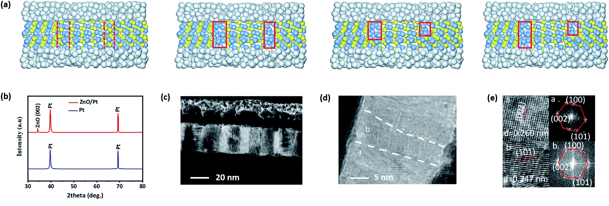 | ||
| Fig. 1 (a) Schematic of the formation of pseudo-straight conductive filaments in Pt/ZnO/Pt resistive switching memristor devices with vertical grain boundaries. (b) XRD patterns of the Pt-coated substrate (blue) and the ZnO nanofilm grown on it (red). (c) TEM image, (d) HRTEM image and (e) zoom-in view of the lattice fringes and fast Fourier transformed images of the as-fabricated Pt/ZnO/Pt device showing columnar ZnO nanocrystals. | ||
Based on this idea, we fabricated a Pt/ZnO/Pt structured device on a commercially available SiO2/Si substrate by magnetron sputtering as described above in the Experimental Methods section. The X-ray diffractive pattern and TEM images indicate that the ZnO nanofilm is (002)-textured and grew into straight columnar microcrystals (Fig. 1b and c). The thicknesses of the as-prepared ZnO nanofilms are ≈30 nm. As marked by the white dashed line in the HRTEM image in Fig. 1d, the vertical grain boundaries propagating along the out-of-plane direction can be clearly identified from the surrounding oxide columnar crystals. On one side of the boundary (region a), the ZnO nanocrystal shows a uniform lattice fringe of (002) planes with a d-spacing of 0.260 nm (upper panels of Fig. 1e), indicating that the particular column has a majority phase of hexagonal wurtzite structure. The corresponding fast Fourier transformed micrograph also verifies this claim. On the other side (region b), although the lattice fringe shows a smaller d-space of 0.247 nm, which indicates observation of the (101) crystal planes (lower panel of Fig. 1e), the fast Fourier transformed micrograph reveals that the crystalline structure of this nano-column is identical to that of region a except for the different grain orientation. Therefore, it can be confirmed that with the present sputtering setups, zinc oxide nanofilms with a hexagonal wurtzite column structure that favors the formation of pseudo-straight conductive filaments can be obtained as expected.
The current–voltage (I–V) curve of the Pt/ZnO/Pt device is shown in Fig. 2a. Three resistive states that are stable and accessible can be obtained by controlling the limiting current during the set process and the cut-off voltage during the reset process. During the set process, the device can be switched from a high resistance state (HRS, 2.5 kΩ to 5.0 kΩ) to a middle resistance state (MRS, 200 Ω to 600 Ω) by sweeping the voltage (applied to TE) from 0 V to 0.8 V with a limiting current of 1 mA (blue curve, sweep 1). Although the device current is limited by the compliance preset, continuous migration of the oxygen species can lead to overgrowth of the conductive filaments, and the device resistance is smaller than the nominal value determined by the I–V curve.38 As such, in sweep 2, the device current (pink curve) departs significantly from the previous level and transits from MRS to a low resistance state (LRS, 30 Ω to 80 Ω) at ∼0.5 V with an increased compliance current of 10 mA. Upon reversing the voltage polarity in the subsequent reset process, sweeping from 0 V to −0.8 V and −1.6 V can reprogram the device resistance state back to the MRS and HRS, respectively (sweeps 3 and 4). It is noteworthy that the present Pt/ZnO/Pt device shows gradual rather than abrupt transitions during the reset processes, which benefits the selection of proper programming voltages to maintain the operation symmetry for logic algorithms. Herein, 0.7 V (Vth1), 1.4 V (Vth2), −0.7 V (−Vth1) and −1.4 V (−Vth2) were employed as the threshold voltages for the device to switch between HRS, MRS, and LRS in subsequent experiments. The switching ratios of both the HRS/MRS and MRS/LRS transitions are close to 10, which provides a good distinction window for the subsequent logic output identification. As shown in Fig. 2b, three-state switching can also be achieved with pulse mode operation, where the black, dashed and red lines represent the input voltage pulses, immediate responding currents and device currents read at 0.2 V, respectively. All these states can be repeatedly programmed and accessed (Fig. 2c) and can be maintained for at least 104 seconds at room temperature (Fig. 2d). The cycle-to-cycle and device-to-device variations of all the programming voltages and HRS/MRS/LRS resistances are less than 7%, which indicates the potential capability of the present device for practical applications. In this work, the pulse voltages applied to either T1 or T2 serve as the univariate input signals, while the value of VT1 − VT2 determines the change of the device resistance in the logic operation. We define V0 = 0 V, V1 = 0.8 V, and V2 = 1.6 V as logic inputs “0”, “1”, and “2” and the high, intermediate and low resistances as the logic outputs “0”, “1”, and “2”, respectively. The output logic (final resistance) state of the memristor is stored directly in the same device and can be read out by an additional independent read step with a small voltage pulse of 0.2 V.
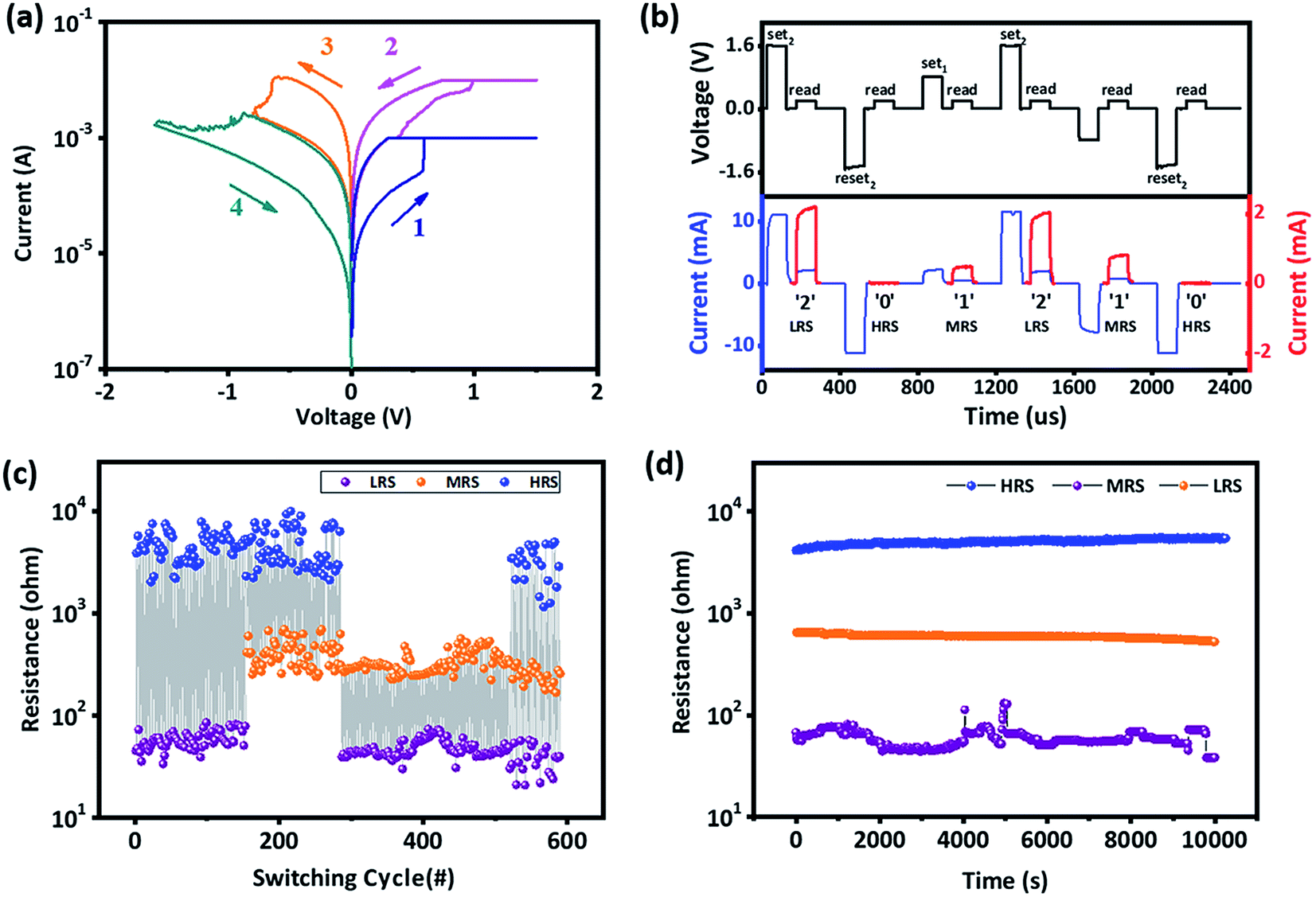 | ||
| Fig. 2 (a) DC current–voltage characteristics and (b) pulse mode response of the Pt/ZnO/Pt memristor showing three-state switching behavior. (c) and (d) show the room-temperature endurance and retention performance of the device, respectively. | ||
Generally, univariate ternary logic consists of 27 functions (f(x) ∈ {0, 1, 2}) and can be classified into several groups.39 Based on the above definitions, all 27 of these operations can be achieved in no more than 3 sequential steps of initializing and writing(s) with a single memristor (Tables S1 and S2†). In practical applications, we only need to select a combination of functions that can form a complete set of three-valued univariate functions (e.g. {f2, f6, f18}, {f21, f9, f18} and {f21, f2, f8}). With the aid of AND and OR operations, certain groups of the univariate functions can be used to form a three-valued functional complete set. When implementing the same function, there are certain differences in the arithmetic complexity of different univariate function combinations. Due to the simple function expression and circuit architecture for the three-valued multiplier, we demonstrate the implementation of literal logics of F2, F6 and F18 as an example. As shown in the truth table of Fig. 3a, upon fixing the initial logic state of the device and one of the terminal voltage inputs, one more step of univariate writing to the other terminal can implement literal logic operations. Herein, the variable q takes the values “0”, “1” or “2”; Vbase is defined as 0.2 V, and Vth2 is defined as 1.4 V.
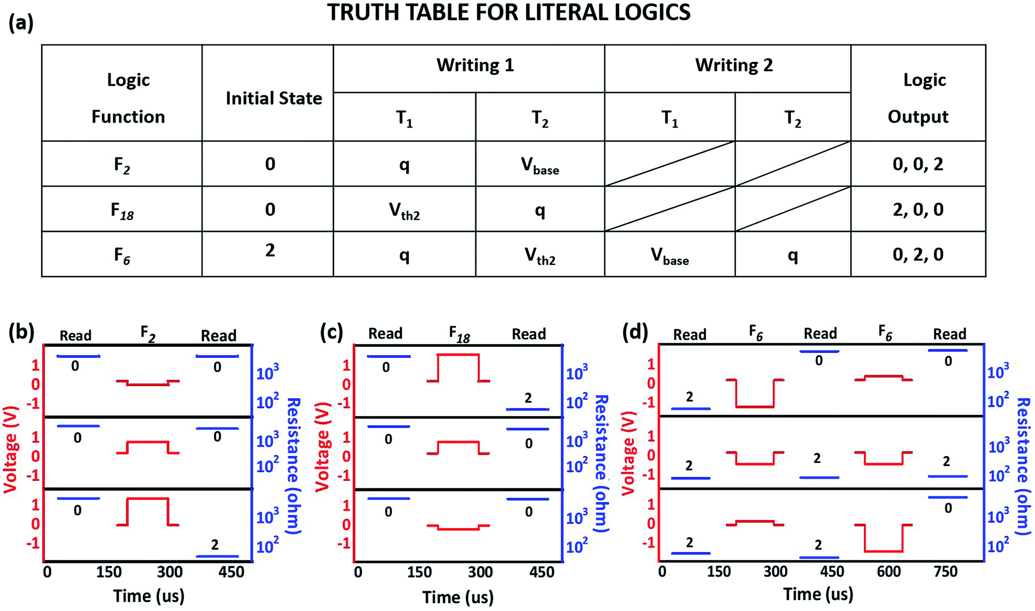 | ||
| Fig. 3 (a) Truth table and (b–d) experimental demonstration of the F2, F18 and F6 literal operations, showing the equivalent voltages and resistances of the memristor. | ||
As a proof-of-concept, we show the experimental implementation of the literal logic in Fig. 3b–d. For logic F2, the ZnO memristor is initially programmed to logic “0” with a resistance of 2.5 kΩ to 5.0 kΩ, and the T2 terminal is fixed as Vbase (Fig. 3b). When voltage pulses with amplitudes of 0 V (logic “0”), 0.8 V (logic “1”) and 1.6 V (logic “1”) are applied to the T1 terminal, respectively, the final resistances of the device are recorded as 3.5 kΩ (logic output “0”), 3.6 kΩ (logic output “0”) and 48 Ω (logic output “2”). Consistent with the results summarized in the truth table, logic function F2 is thus achieved with a two-step operation (initial = “0”, T1 = q, T2 = Vbase). Logic F18 can be realized similarly by fixing the initial logic state of the memristor as “0” and the T1 terminal as Vth2 and applying writing voltage variables q to T2. To achieve logic F6, one more writing step is necessary: the memristor is first initialized to logic “2”; then, T2 is fixed as Vth2 while T1 is written with the voltage variable q; finally, T1 is fixed as Vbase, and T2 is written with the voltage variable q. As such, F6 is implemented through a three-step operation.
To form the functional complete logic set, we demonstrate the truth table and operation method of the AND and OR operations in Fig. 4. In the AND operation, after the device is initialized to logic “0”, input p is first written at T1 while T2 is grounded; then, input q is written into T1, and T2 is fixed at V2 (Fig. 4a). The actual equivalent voltages (VT1 − VT2) applied to the memristor and the corresponding resistance states during the p/q input process are sequentially shown in Fig. 4c, confirming the realization of the AND operation in the present ternary scheme. Similarly, Fig. 4b provides the truth table and operation method for OR operation, and Fig. 4d shows the actual equivalent voltages applied to the memristor and the changes in device resistance during execution.
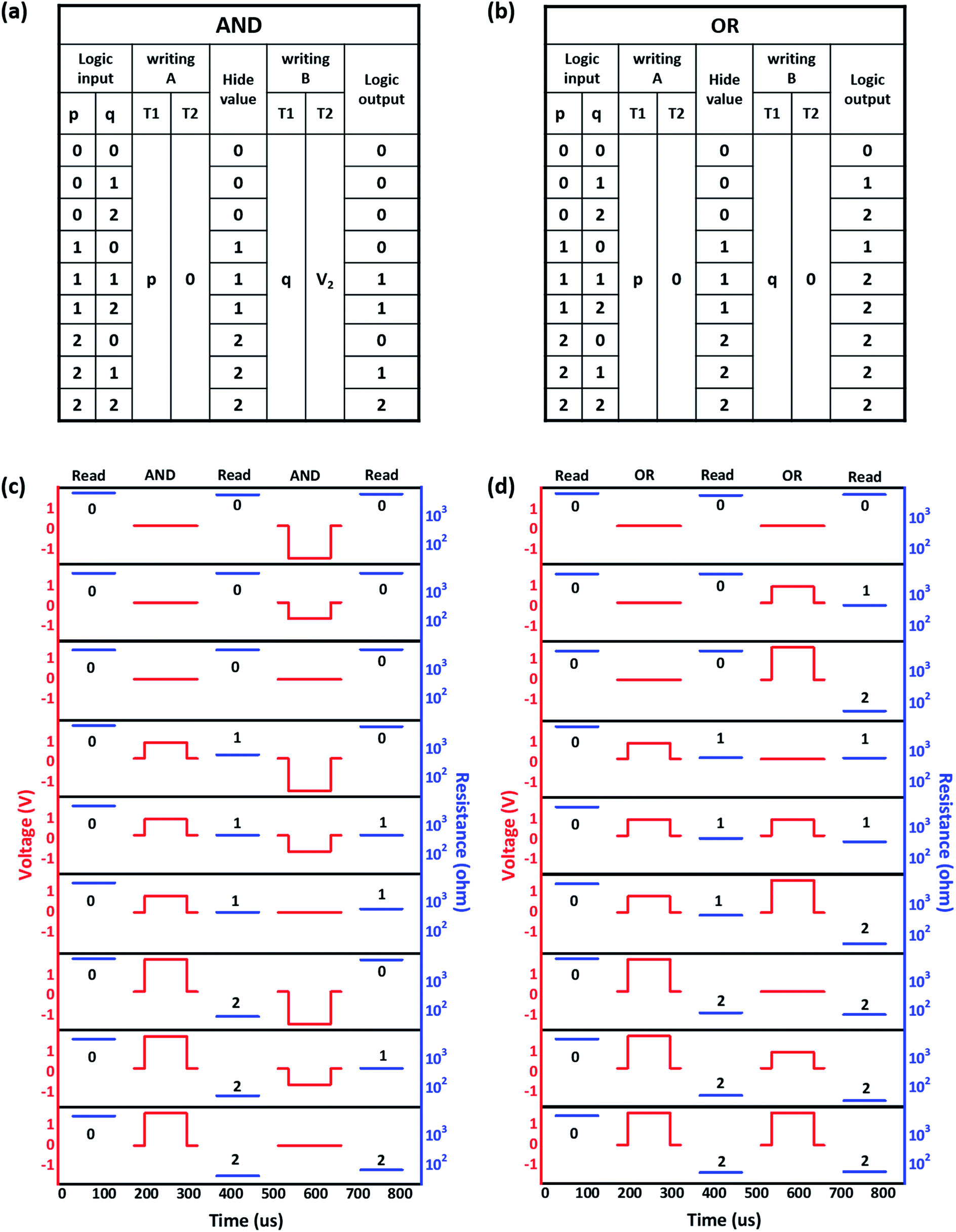 | ||
| Fig. 4 (a and b) Truth table and (c and d) experimental demonstration of the AND and OR operations showing the equivalent voltages and resistances of the memristor. | ||
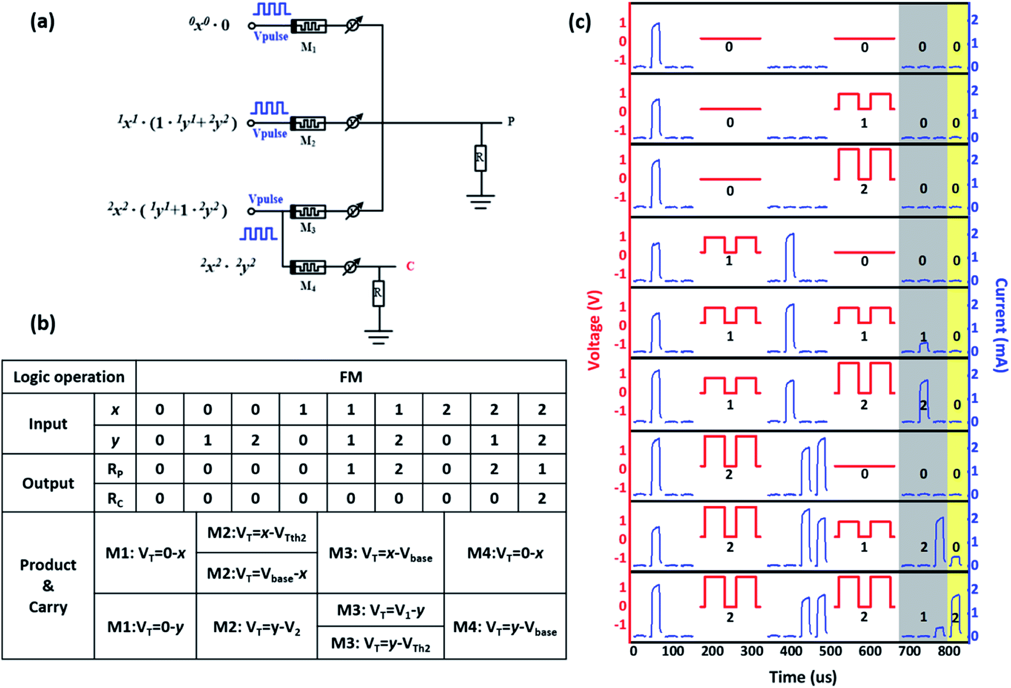
Based on the functional complete logic set of the literal logics of F2, F6 and F18 and the AND and OR operators, a simple three-valued multiplier circuit was designed with four ZnO-based memristors (Fig. 5a). Herein, the memristors M1, M2, and M3 are responsible for multiplication, while M4 is responsible for the bit-carry operation. The multiplicand and multiplier are defined as logic inputs A and B, respectively. Note that the logic state of the HRS/LRS device will not change even when continuous negative/positive voltages are applied to the ZnO memristor. We used this characteristic to stop M2 and M3 from working when the multiplicand input A = 0; thus, only M1 was functional. Similarly, when the A inputs are “1” and “2”, the working devices are M2 and M3, respectively. In other words, the Mi (i = 1, 2, 3) device is responsible for the multiplication of the multiplicand A = “i − 1”. The ternary multiplier produces a carry output only when both the multiplicand A and the multiplier B are equal to 2; therefore, it is only necessary to store the carry output value with the M4 device in the M3 branch. Because the carry signal in the multi-valued logic is a binary signal, e.g. the product output at C is a binary digit, the carry operation is only performed when the output of M4 is logic “2”. Otherwise, it is not carried. After the calculation is completed, the current value read by the small voltage can be used as the output result. The truth table and operation method of the full multiplier (FM) are shown in Fig. 5b. Due to the two-step implementation of the univariate function, bimodal pulse input is used during the operation. Fig. 5c shows the experimental FM operation, wherein the red and blue lines represent the operating pulse voltage and current response on the memristor. The four blue current curves are the current responses of M1 to M4. The gray area (M1 to M3) represents the multiplier result value output, and the yellow area (M4) is the carry output.
 | ||
| Fig. 5 (a) Circuit structure diagram of the three-valued multiplier unit based on ZnO memristors. (b) The truth table, operation method and (c) experimental demonstration of the full multiplier operation. | ||
4. Conclusion
We produced a bipolar three-state memristor device with columnar nanocrystalline zinc oxide as the switching layer to obtain symmetric resistive switching characteristics and proposed a simple approach to implement ternary logics. Through univariate operation in no more than three steps of initializing and writing(s), literal AND and OR operations can be achieved with a single device to form a functional complete three-valued logic set. Based on this, four memristors were used to design a three-value multiplier unit. In addition to the in-memory computing capabilities, the higher order computation scheme with the present ternary routes may further enhance the efficiency of in-memory computing with reduced wire connections and lower chip areas. By including materials with high dielectric constants or optimizing the thickness and microstructure of the switching matrix, the device current can be further lowered to enhance the energy efficiency of in-memory computing with resistive switching memristors.Availability of data and materials
All data are fully available without restriction.Conflicts of interest
The authors declare that they have no competing interests.Acknowledgements
This work was sponsored by the National Key R&D Program of China (2017YFB0405600 and 2017YFF0105000), National Natural Science Foundation of China (11832016, 61722407, 51775471, 61674153 and 51525103), Program for Changjiang Scholars, Provincial Natural Science Foundation of Hunan (2018JJ4037) and the Innovative Research Team in University (IRT-14R48), and the Hunan Provincial Innovation Foundation for Postgraduate (No. CX2018B373).References
- K. Bernstein, R. K. Cavin, W. Porod, A. Seabaugh and J. Welser, Proc. IEEE, 2010, 98, 2169–2184 Search PubMed.
- L. O. Chua, IEEE Trans. Circuit Theory, 1971, 18, 507–519 Search PubMed.
- D. B. Strukov, G. S. Snider, D. R. Stewart and R. S. Williams, Nature, 2008, 453, 80–83 CrossRef CAS PubMed.
- J. Borghetti, G. S. Snider, P. J. Kuekes, J. J. Yang, D. R. Stewart and R. S. Williams, Nature, 2010, 464, 873–876 CrossRef CAS PubMed.
- J. J. Yang, D. B. Strukov and D. R. Stewart, Nat. Nanotechnol., 2013, 8, 13–24 CrossRef CAS PubMed.
- D. Ielmini and H. S. P. Wong, Nat. Electron., 2018, 1, 333–343 CrossRef.
- M. A. Zidan, J. P. Strachan and W. D. Lu, Nat. Electron., 2018, 1, 22–29 CrossRef.
- I. Vourkas and G. C. Sirakoulis, IEEE Circuits Syst. Mag., 2016, 16, 15–30 Search PubMed.
- M. Teimoory, A. Amirsoleimani and J. Shamsi, Comput. Sci., 2015, 562–565 Search PubMed.
- T. Breuer, A. Siemon, E. Linn, S. Menzel, R. Waser and V. Rana, Adv. Electron. Mater., 2015, 1, 1500138 CrossRef.
- P. Yao, H. Q. Wu, B. Gao, S. B. Eryilmaz, X. Y. Huang, W. Q. Zhang, Q. T. Zhang, N. Deng, L. P. Shi, H. S. Philip Wong and H. Qian, Nat. Commun., 2017, 8, 15199 CrossRef CAS PubMed.
- Y. Li, Y. X. Zhou, L. Xu, K. Lu, Z. R. Wang, N. Duan, L. Jiang, L. Cheng, T. C. Chang, K. C. Chang, H. J. Sun, K. H. Xue and X. S. Miao, ACS Appl. Mater. Interfaces, 2016, 8, 34559–34567 CrossRef CAS PubMed.
- S. Gao, G. Liu, Q. Chen, W. Xue, H. Yang, J. Shang and R. W. Li, ACS Appl. Mater. Interfaces, 2018, 10, 6453–6462 CrossRef CAS PubMed.
- T. You, Y. Shuai, W. Luo, N. Du, D. Burger, I. Skorupa and T. Mikolajick, Adv. Funct. Mater., 2014, 24, 3357–3365 CrossRef CAS.
- F. Zhou, L. Guckert, Y. F. Chang, E. E. Swartzlander and J. Lee, Appl. Phys. Lett., 2015, 107, 183501 CrossRef.
- G. C. Adam, B. D. Hoskins, M. Prezioso and D. B. Strukov, Nano Res., 2016, 9, 1–10 CrossRef.
- E. Linn, R. Rosezin, S. Tappertzhofen, U. Böttger and R. Waser, Nanotechnology, 2012, 23, 305205 CrossRef CAS PubMed.
- P. M. Sheridan, F. Cai, C. Du, W. Ma, Z. Zhang and W. D. Lu, Nat. Nanotechnol., 2017, 12, 784–789 CrossRef CAS PubMed.
- H. Li, B. Gao, Z. Chen, Y. Zhao, P. Huang, H. Ye and J. Kang, Sci. Rep., 2015, 5, 13330 CrossRef CAS PubMed.
- G. S. Park, X. S. Li, D. C. Kim, R. J. Jung, M. J. Lee and S. Seo, Appl. Phys. Lett., 2007, 91, 1129 Search PubMed.
- M. Lanza, G. Bersuker, M. Porti, E. Miranda, M. Nafría and X. Aymerich, Appl. Phys. Lett., 2012, 101, 193502 CrossRef.
- H. Woo, S. K. Vishwanath and S. Jeon, ACS Appl. Mater. Interfaces, 2018, 10, 8124–8131 CrossRef CAS PubMed.
- J. Shang, G. Liu, H. Yang, X. Zhu, X. Chen, H. Tan, B. Hu, L. Pan, W. Xue and R.-W. Li, Adv. Funct. Mater., 2014, 24, 2171–2179 CrossRef CAS.
- J. Shang, W.-H. Xue, Z.-H. Ji, G. Liu, X. H. Niu, X. H. Yi, L. Pan, Q.-F. Zhan, X. H. Xu and R.-W. Li, Nanoscale, 2017, 9, 7037–7046 RSC.
- Q. Chen, G. Liu, W. Xue, J. Shang, S. Gao, X. Yi, Y. Lu, X. Chen, M. Tang, X. Zheng and R.-W. Li, ACS Appl. Electron. Mater., 2019 DOI:10.1021/acsaelm.9b00191.
- N. Xu, L. F. Liu, X. Sun, X. Y. Liu and D. D. Han, Appl. Phys. Lett., 2008, 92, 232112 CrossRef.
- Y. Yang, H. Long, G. Yang, A. Chen, Q. Zheng and P. Lu, Femtosecond laser deposited zinc oxide film and its optical properties, Vacuum, 2009, 83, 892–896 CrossRef CAS.
- A. Chen, Z. Bi, C.-F. Tsai, J. H. Lee, Q. Su, X. Zhang and Q. Jia, Adv. Funct. Mater., 2011, 21, 2423–2439 CrossRef CAS.
- Y. C. Yang, X. X. Zhang, M. Gao, F. Zeng, W. Y. Zhou, S. S. Xie and F. Pan, Nanoscale, 2011, 3, 1917–1921 RSC.
- M. H. Tang, B. Jiang, Y. G. Xiao, Z. Q. Zeng, Z. P. Wang, J. C. Li and J. He, Microelectron. Eng., 2012, 93, 35–38 CrossRef CAS.
- Z. Q. Wang, H. Y. Xu, L. Zhang, X. H. Li, J. G. Ma, X. T. Zhang and Y. C. Liu, Nanoscale, 2013, 5, 4490–4494 RSC.
- W. H. Xue, W. Xiao, J. Shang, X. X. Chen, X. J. Zhu, L. Pan, H. W. Tan, W. B. Zhang, Z. H. Ji, G. Liu, X.-H. Xu, J. Ding and R.-W. Li, Nanotechnology, 2014, 25, 425204 CrossRef CAS PubMed.
- S. Vallejos, N. Pizúrová, I. Gràcia, C. Sotelo-Vaquez, J. Čechal, C. Blackman, I. Parkin and C. Cané, ACS Appl. Mater. Interfaces, 2016, 8, 33335–33342 CrossRef CAS PubMed.
- M. Pea, G. Barucca, A. Notargiacomo, L. Di Gaspare and V. Mussi, Appl. Surf. Sci., 2018, 433, 899–903 CrossRef CAS.
- D. Barreca, G. Carraro, C. Maccato, T. Altantzis, K. Kaunisto and A. Gasparotto, Cryst. Growth Des., 2018, 18, 2579–2587 CrossRef CAS.
- H.-P. Hsu, D.-Y. Lin, C.-Y. Lu, T.-S. Ko and H.-Z. Chen, Crystals, 2018, 8, 228 CrossRef.
- M. Schie, M. P. Müller, M. Salinga, R. Waser and R. A. De Souza, J. Mater. Chem. C, 2017, 146, 094508 Search PubMed.
- W. Xue, G. Liu, Z. Zhong, Y. Dai, J. Shang, Y. Liu, H. Yang, X. Yi, H. Tan, L. Pan, S. Gao, J. Ding, X.-H. Xu and R.-W. Li, Adv. Mater., 2017, 29, 1702162 CrossRef PubMed.
- M. Goto, Y. Komamiya, R. Suekane, M. Takagi and R. Kuwabara, Theory and structure of the automatic relay computer ETL mark II, 1958, DOI:10.2307/2964501.
Footnote |
| † Electronic supplementary information (ESI) available. See DOI: 10.1039/c9ra04119b |
| This journal is © The Royal Society of Chemistry 2019 |