DOI:
10.1039/C9RA03574E
(Paper)
RSC Adv., 2019,
9, 27117-27124
Approaching subthreshold-swing limit for thin-film transistors by using a giant-dielectric-constant gate dielectric†
Received
13th May 2019
, Accepted 19th August 2019
First published on 28th August 2019
Abstract
Low-temperature giant-dielectric-constant thin films (In0.0025Nb0.0025Ti0.995O2) fabricated with simple radio frequency (RF) sputtering on glass substrates are employed as the gate dielectrics for thin-film transistors (TFTs) for the first time. The 380 nm-thick In0.0025Nb0.0025Ti0.995O2 film exhibited a quasi-static capacitance of as high as 36![[thin space (1/6-em)]](https://www.rsc.org/images/entities/char_2009.gif) 156 nF cm−2 with a quasi-static permittivity of 15525 (and 7607 nF cm−2 at 1 kHz). Indium zinc oxide (IZO) TFTs with In0.0025Nb0.0025Ti0.995O2 gate dielectrics exhibited high output current at low operation voltage and little hysteresis in the transfer curves between forward and reverse sweeps. The subthreshold swing (SS) of the IZO TFTs is 0.068 V dec−1, very close to the lowest limit of the SS of the field-effect transistors (0.06 V dec−1). The results also proves that the lowest limit of the SS (0.06 V dec−1) cannot be broken no matter how high the gate dielectric capacitance is (except for negative capacitors). The TFTs demonstrate the potential for the applications in low-power circuits or flat-panel displays.
156 nF cm−2 with a quasi-static permittivity of 15525 (and 7607 nF cm−2 at 1 kHz). Indium zinc oxide (IZO) TFTs with In0.0025Nb0.0025Ti0.995O2 gate dielectrics exhibited high output current at low operation voltage and little hysteresis in the transfer curves between forward and reverse sweeps. The subthreshold swing (SS) of the IZO TFTs is 0.068 V dec−1, very close to the lowest limit of the SS of the field-effect transistors (0.06 V dec−1). The results also proves that the lowest limit of the SS (0.06 V dec−1) cannot be broken no matter how high the gate dielectric capacitance is (except for negative capacitors). The TFTs demonstrate the potential for the applications in low-power circuits or flat-panel displays.
1. Introduction
The gate dielectric is important for a thin-film transistor (TFT), because the performance of the TFT device is affected by the interface/bulk traps, interface coupling, dielectric constant, leakage current, and breakdown field of the gate dielectric. For applications in active-matrix (AM) displays, especially for the AM organic light-emitting diode (OLED) displays, TFTs should be of high output current at relatively low operation voltage to meet the driving current of the OLEDs and reduce the power consumption. In AMOLEDs, the total power consumption (Ptotal) of each pixel mainly depends on the OLED power consumption (POLED) and the TFT power consumption (PTFT):| | |
Ptotal ≈ ηvideo × (POLED + PTFT) ∝ (VOLED + VTFT)
| (1) |
where ηvideo is the percentage of on state of the pixels during the video operation, VOLED is the voltage drop of the OLED, and VTFT is the voltage drop of the TFT. It has been reported that PTFT can be greater than 50% of Ptotal when the mobility is lower than 5 cm2 V−1 s−1.1 Therefore, reducing the operation voltage of TFTs is an effective way for reducing the power consumption for AMOLEDs.
As known, the operation voltage of TFTs is determined by subthreshold swing (SS), which is defined as the change in gate voltage (VG) required for one order change in the drain current (ID). TFTs with lower SS usually have lower operation voltage. To lower the operation voltage and SS, fabricating TFTs with high-capacitance gate dielectric is the topic intriguing researchers in the industry and academia. Generally, there are two ways to increase the capacitance of the gate dielectrics—reducing the thickness or increasing the dielectric constant (k) of the gate dielectrics. For practical application to active-matrix displays, the thickness of the gate dielectrics of TFTs should be greater than 200 nm to avoid electrical breakdown in the whole panel. In this case, further reducing the dielectric thickness to less than 200 nm would risk increasing of defects in the displays. Therefore, employing high dielectric constant dielectrics to increase the capacitance is preferred. Various high-k dielectric materials have been applied to TFTs, such as HfO2, Al2O3 and etc.2,3 However, the dielectric constants of most of the high-k materials are less than 40. So these materials have a limited effect of reducing the operating voltage of the transistors.
At the same time, some research teams employed ferroelectrics as the gate dielectrics,4,5 such as BaTiO3 (BTO, kbulk ∼103; kfilm ∼500), Pb(Zr,Ti)O3 (PZT, kbulk ∼103; kfilm ∼800) and etc.6–9 However, the dielectric constant of the spontaneous-polarization ferroelectrics relies seriously on the temperature and the electric field applied to the ferroelectrics, causing uncertain response when writing data signal to the TFTs.
Recently, a new type of transistors, named electric-double-layer (EDL) transistors, have been investigated as a candidate for low-voltage application by using polymer electrolytes or ionic liquids as gate dielectrics.10–12 In such transistors, a high gate capacitance can be obtained by mobile ions that are able to move to form EDL, whose capacitance can be higher than 1 μF cm−2 at low frequency. However, the speed of the ions is usually too slow for active-matrix displays, whose frame rate is ∼50–500.
In 2000, Subramanian et al. found the “giant dielectric behaviour” (kbulk > 104) in CaCu3Ti4O12 ceramics,13 which triggers a large number of studies on giant dielectric materials, e.g., A2/3Cu3Ti4O12 (A = Bi, La, Y), (Li, Ti) co-doped NiO, (In, Nb) co-doped TiO2 (kbulk ∼104; kfilm ∼4000), etc.14–18 However, attaining “giant dielectric” phase requires well-controlled deposition processes, specify substrates, and high annealing temperature (>1000 °C), which is beyond the upper limit of glass substrates for TFTs.
In this paper, we demonstrate low-temperature (400 °C) giant-dielectric-constant thin films (In0.0025Nb0.0025Ti0.995O2) fabricated with simply radio frequency (RF) sputtering method for the gate dielectrics of the indium–zinc-oxide (IZO) TFTs on glass substrates. The 380 nm-thick In0.0025Nb0.0025Ti0.995O2 film exhibited a capacitance of as high as 7607 nF cm−2 with a permittivity of 3266 at 1 kHz. IZO-TFTs with In0.0025Nb0.0025Ti0.995O2 gate dielectrics exhibited high output current at low operation voltage and little hysteresis in the transfer curves between forward and reverse sweeps. The micro structures and the mechanisms of the giant dielectric behaviour at low annealing temperature were discussed.
2. Experimental
2.1. Device preparation
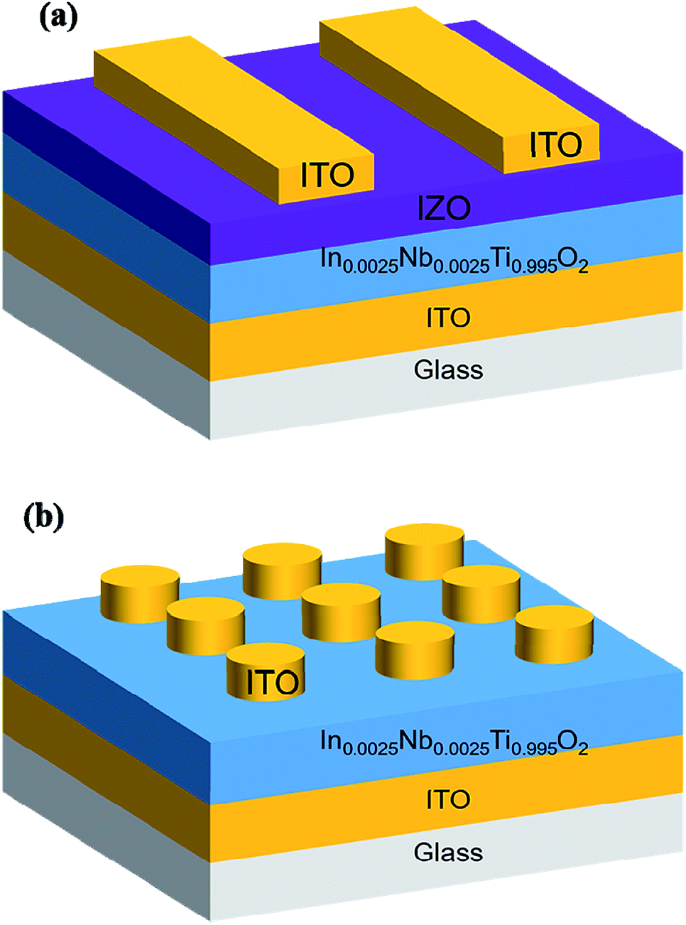
The device structure of the IZO TFTs is shown in Fig. 1a. A layer of 150 nm-thick indium–tin-oxide (ITO, In:Sn = 9:1) gate electrode was fabricated on a glass substrate by direct current sputtering. Then, a layer of 380 nm-thick In0.0025Nb0.0025Ti0.995O2 film acting as the gate dielectric layer was deposited by RF magnetron sputtering with the In0.0025Nb0.0025Ti0.995O2 ceramics target under argon pressure of 0.5 Pa, and annealed in air at 400 °C for 30 minutes. The IZO (In:Zn = 2:1) semiconductor layer was deposited onto the gate dielectric layer by RF magnetron sputtering and annealed in air at 300 °C for 30 minutes. For the source and drain electrodes, a layer of 110 nm-thick ITO was deposited through a shadow mask, defining a channel width/length of 800/200 μm. Finally, the TFTs were annealed in air at 300 °C for 30 minutes. In addition, the metal–insulator–metal (MIM) capacitors were fabricated (see Fig. 1b).
 |
| | Fig. 1 Schematic structures of (a) the TFT with In0.0025Nb0.0025Ti0.995O2 gate insulator and (b) the capacitors with ITO/In0.0025Nb0.0025Ti0.995O2/ITO stacks. | |
2.2. Characterization
The In0.0025Nb0.0025Ti0.995O2 film structure and morphology were characterized by X-ray diffraction (XRD, Bruker D8 ADVANCE) and scanning electron microscopy (SEM, Zeiss Merlin), respectively. The chemical valence of each element of the In0.0025Nb0.0025Ti0.995O2 film was characterized by X-ray photoelectron spectroscopy (XPS, Thermo Fisher Scientific Inc, ESCALAB 250Xi), and the spectra were calibrated with the C 1s peak (at 284.8 eV). Transmission electron microscopy (TEM, FEI Titan Themis 200) specimens of the TFT device was prepared by focused ion beam (FIB, HELIOS NANOLAB 450S). The electrical performance of the TFTs and the MIM capacitors were measured by semiconductor parameter analyzer (Keysight B1500A).
3. Results and discussion
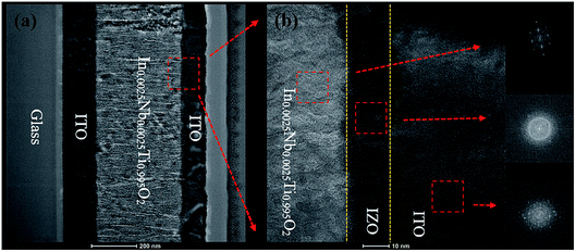
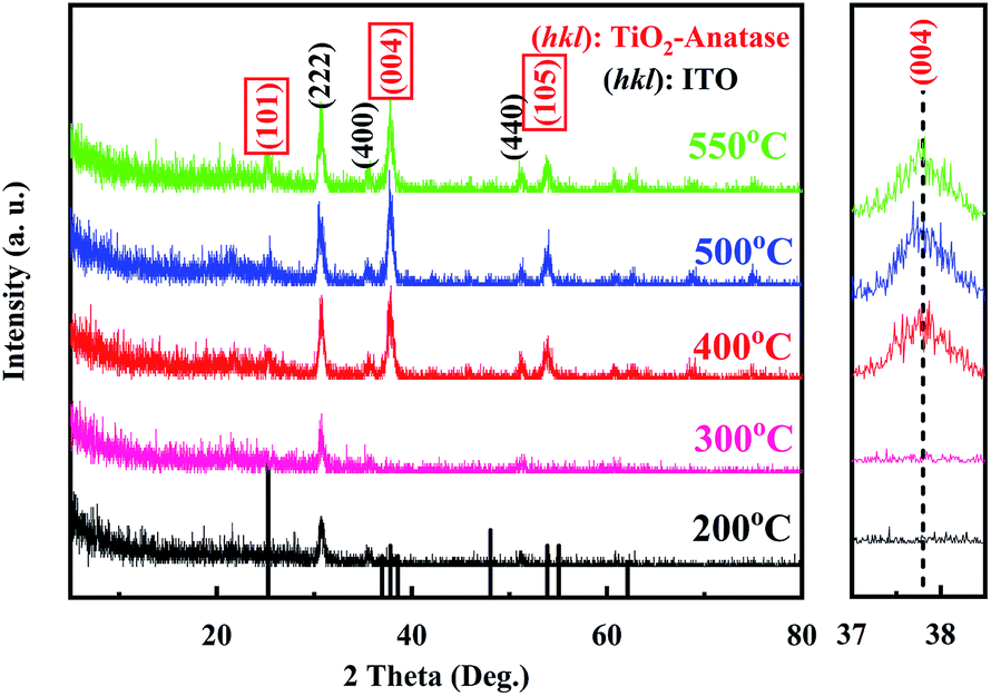
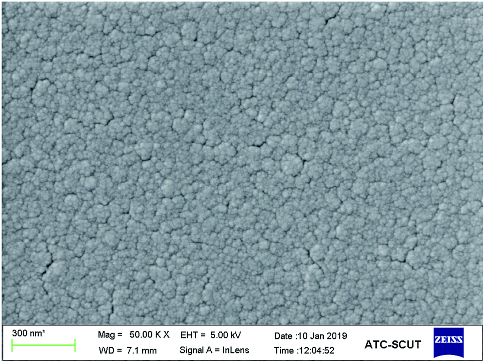
Fig. 2 shows XRD patterns of In0.0025Nb0.0025Ti0.995O2 films on the ITO/glass substrates at different annealing temperatures. The black strips at the bottom of Fig. 2 are the diffraction peaks for the standard anatase phase. For the films annealed at 200 °C and 300 °C, the diffraction peaks of anatase phase could hardly be found, indicating that the In0.0025Nb0.0025Ti0.995O2 films were amorphous. When the annealing temperature increase to 400 °C, the peaks of TiO2-anatase phase (including (101), (004), and (105))19 were observed, indicating that the In0.0025Nb0.0025Ti0.995O2 films begin to crystallize. The strongest diffraction peak for the In0.0025Nb0.0025Ti0.995O2 films was peak (004), which was the third strongest diffraction peak for the standard anatase phase, indicating that the films crystallized with high c-axis orientation. The average crystalline sizes for the films annealing at 400 °C, 500 °C, 550 °C, were calculated to be about 15.2 nm, 16.5 nm and 17.4 nm, respectively, by using the Scherer equation. The diffraction peaks (including (222), (400), (440))20 of the In2O3 bixbyite phase were seem at the annealing temperature of 200 °C, showing that the ITO films were easily to be crystallized even at low annealing temperature. The SEM image (Fig. 3) also showed that the In0.0025Nb0.0025Ti0.995O2 film annealed at 400 °C were in polycrystalline state, which was consistent with the Fast Fourier Transform (FFT) patterns of the high-resolution transmission electron microscopy (HR-TEM) as discussed below.
 |
| | Fig. 2 XRD patterns of the In0.0025Nb0.0025Ti0.995O2 films on ITO/glass substrates annealing at 200 °C, 300 °C, 400 °C, 500 °C and 550 °C. | |
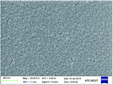 |
| | Fig. 3 SEM image of the In0.0025Nb0.0025Ti0.995O2 film on ITO/glass substrates annealed at 400 °C for 30 minutes. | |
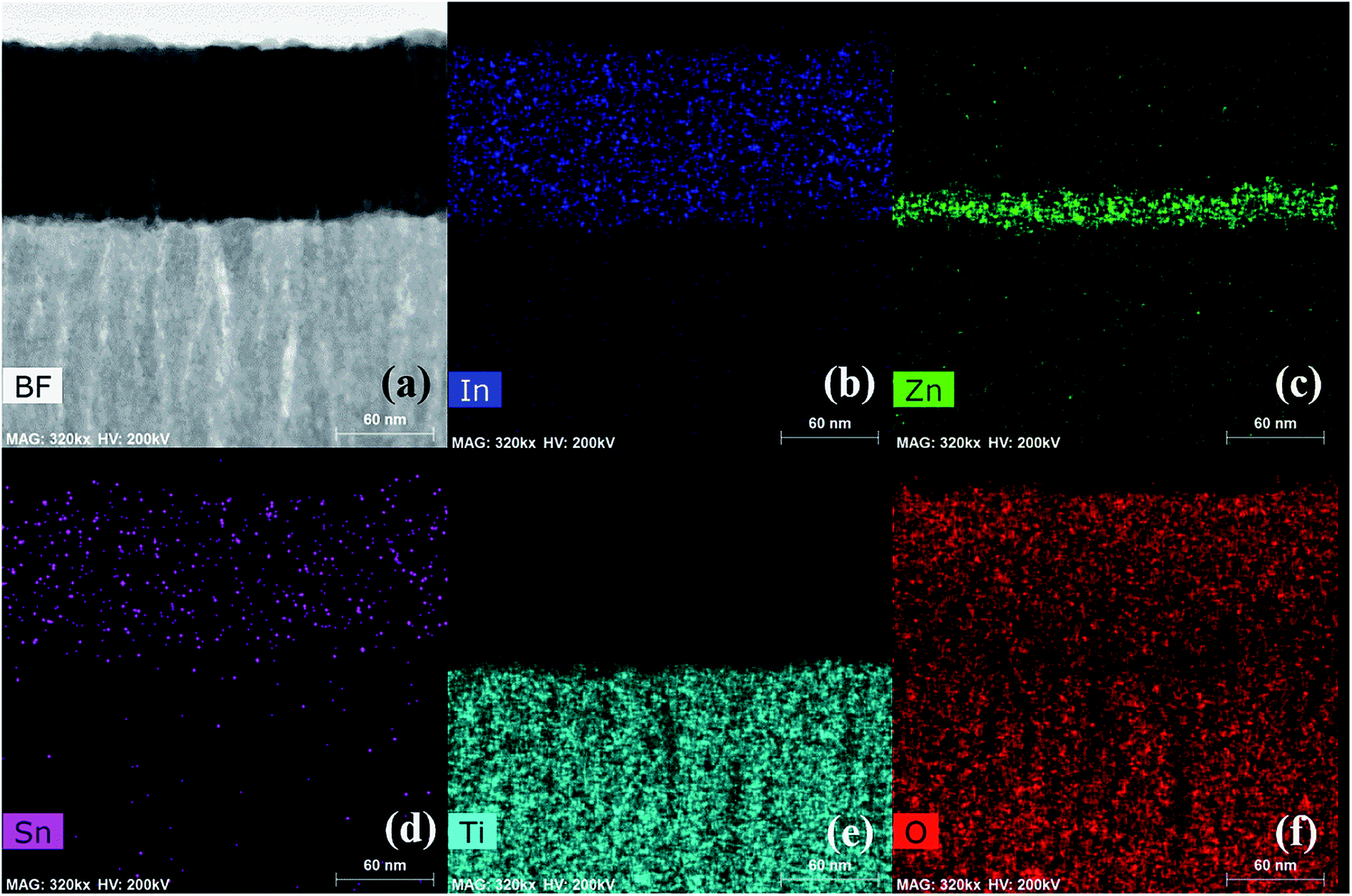
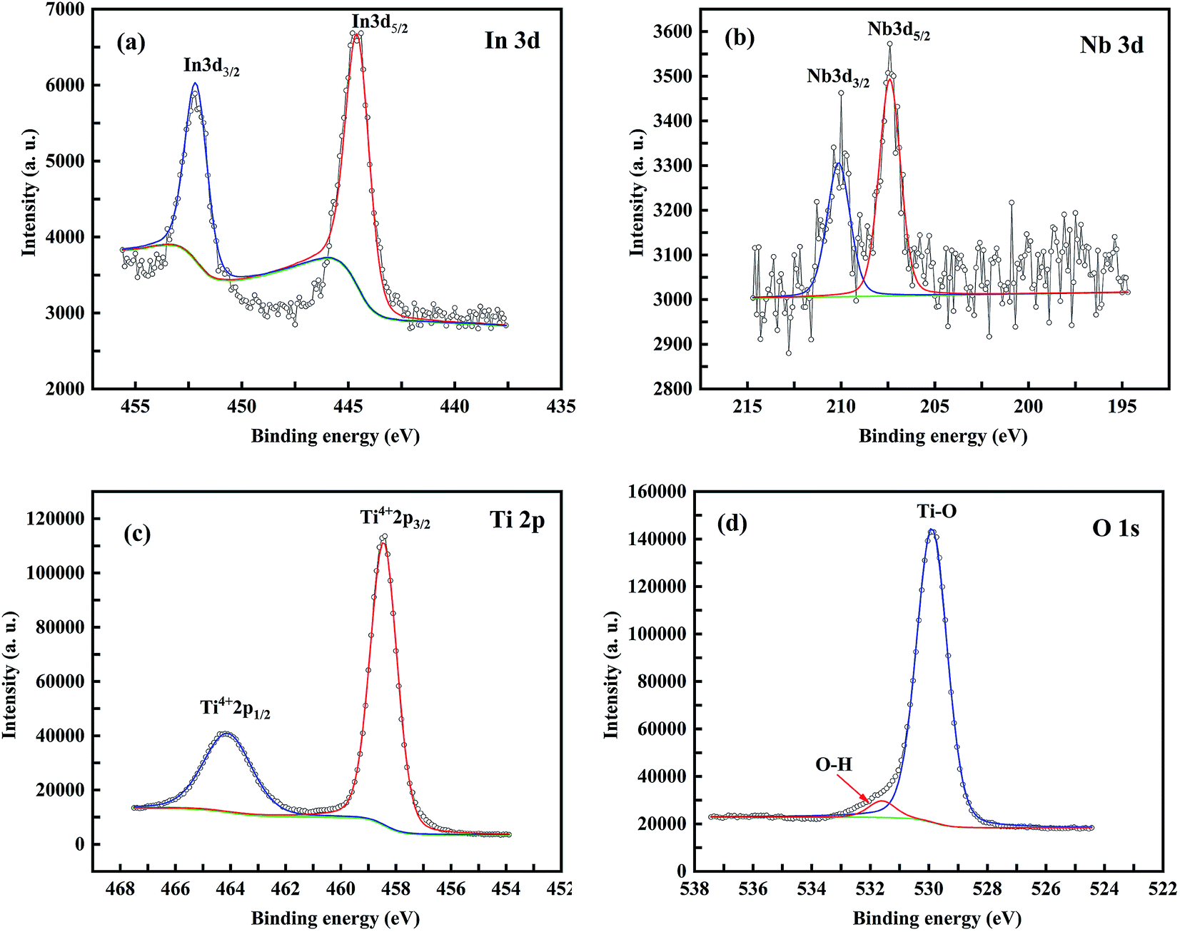
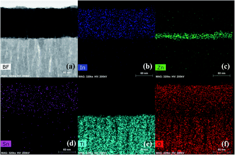
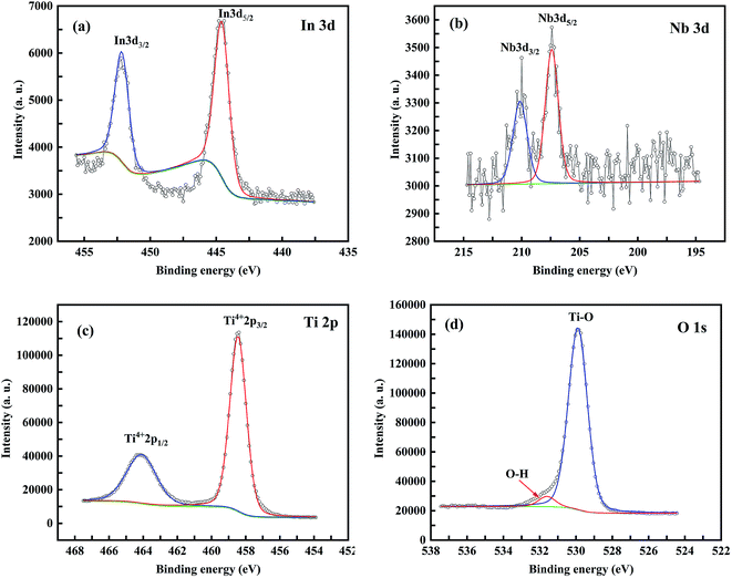
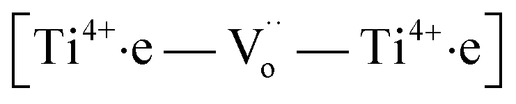
Fig. 4a shows the scanning transmission electron microscopy (STEM) result of the cross-section of the glass/ITO/In0.0025Nb0.0025Ti0.995O2/IZO/ITO structure. Fig. 4b shows the HR-TEM image and the FFT patterns of the In0.0025Nb0.0025Ti0.995O2/IZO/ITO region in Fig. 4a. It was found that both of the In0.0025Nb0.0025Ti0.995O2 and ITO layers were crystallized, while the IZO film was in amorphous state. Fig. 5a–e show the high-angle annular dark-field (HAADF) STEM and elements distribution map obtained from energy-dispersion X-ray spectroscopy (EDS) of the In0.0025Nb0.0025Ti0.995O2/IZO/ITO region. It could be seen that the elements were distributed uniformly in each film without segregated clusters. Because the signals of the elements (In and Nb) are too weak to be detected by EDS, they were characterized by XPS, as shown in Fig. 6a and b. The binding energies of In 3d electrons are 452.4 eV and 444.6 eV for 3d3/2 and 3d5/2, respectively,21 while the binding energies of Nb 3d electrons are 210.1 eV and 207.3 eV for 3d3/2 and 3d5/2, respectively. And the spin orbit splitting between the Nb 3d3/2 and 3d5/2 was 2.8 eV, showing that the valence of Nb in the In0.0025Nb0.0025Ti0.995O2 was +5.22 Fig. 6c shows the binding energy spectra for the Ti 2p electrons (464.10 eV and 458.45 eV are for 2p1/2 and 2p3/2, respectively).22,23 The doublet separation of Ti 2p1/2 and 2p3/2 peaks was 5.65 eV, which shows that the Ti4+ was the main state. Fig. 6d shows the XPS spectra for O 1s. The peak at 529.84 eV was related to the Ti–O bonds while the peak at 531.4 eV was related to the oxygen vacancies or hydroxyl (OH) groups.24 The results indicate that 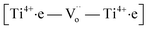 -related defects can be formed.17 However, no peaks related to Ti3+ was observed. It means that the giant dielectric behaviour of In0.0025Nb0.0025Ti0.995O2 was not due to the electron hoping between Ti4+ and Ti3+, which will be discussed later.
 |
| | Fig. 4 (a) Cross-sectional STEM image of the Glass/ITO/In0.0025Nb0.0025Ti0.995O2/IZO/ITO sample annealed at 400 °C for 30 minutes; (b) the HR-TEM image of the In0.0025Nb0.0025Ti0.995O2/IZO/ITO region; the insets of (b) is the FFTs of the region of In0.0025Nb0.0025Ti0.995O, IZO and ITO. | |
 |
| | Fig. 5 (a) HAADF STEM images with elemental distribution detected by EDS for (b) In, (c) Zn, (d) Sn, (e) Ti, (f) O. | |
 |
| | Fig. 6 XPS spectra of the In0.0025Nb0.0025Ti0.995O2 films on ITO/glass substrates annealed at 400 °C for 30 minutes, including: (a) In 3d, (b) Nb 3d, (c) Ti 2p, (d) O 1s. | |
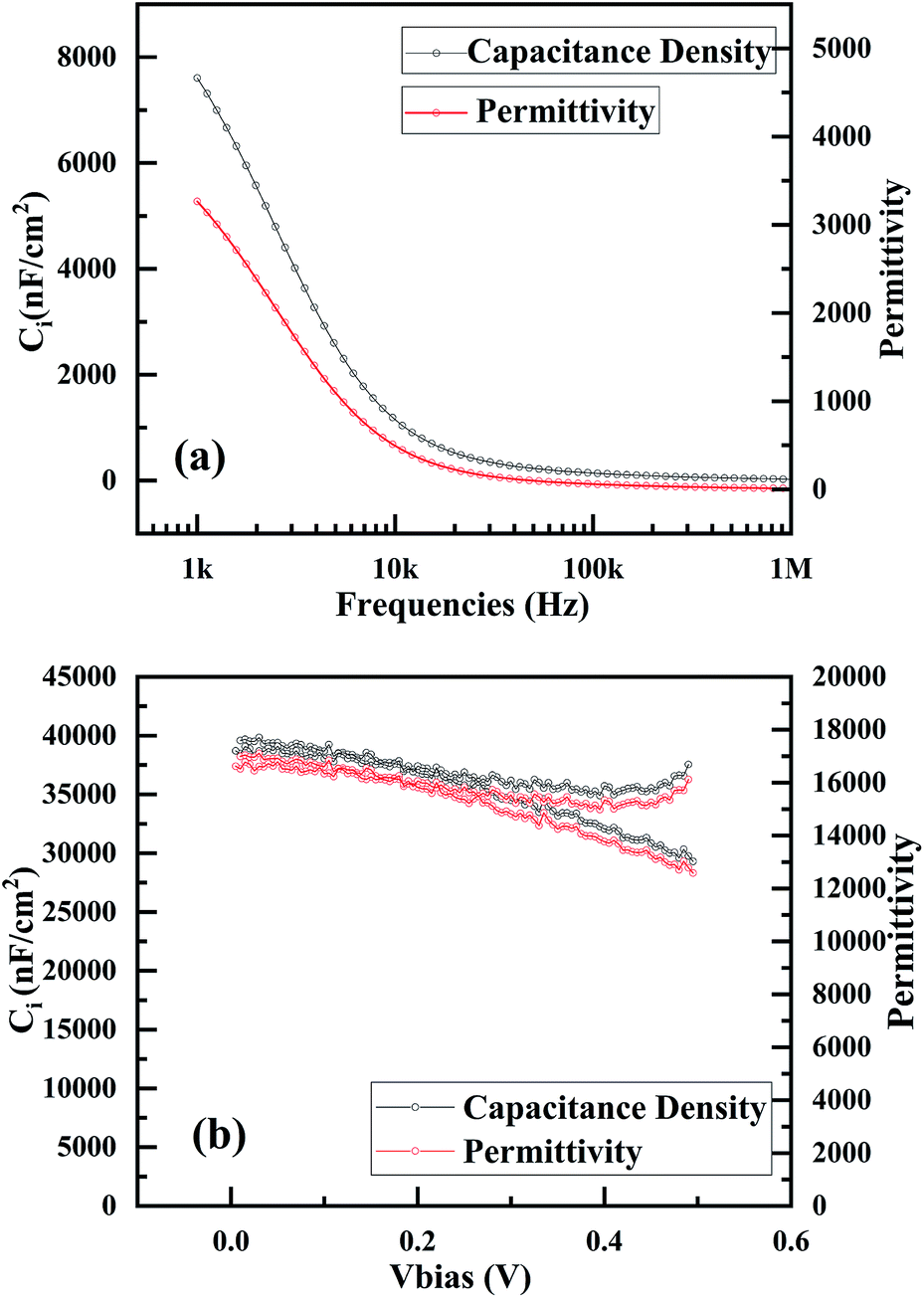
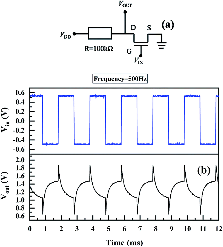
Fig. 7a shows the frequency dependences of capacitance and permittivity of the ITO/In0.0025Nb0.0025Ti0.995O2/ITO capacitors. The areal capacitance (Ci) was as high as 7607 nF cm−2 with a corresponding permittivity of 3266 at 1 kHz (the measured quasi-static Ci was about 36156 nF cm−2 with a quasi-static permittivity of 15525), as shown in Fig. 7b. But the permittivity reduced rapidly when the frequency increased from 1 kHz to 10 kHz, which is inconsistent with the single-crystal TiO2-based giant dielectrics.25 The strongly-frequency-dependent permittivity was ascribed to the extrinsic polarization mechanism, in which the electrons accumulated near the grain boundaries (see Fig. 3) and causing space-charge polarization. Although the permittivity reduced rapidly at higher frequency, the highest frequency required for the active-matrix displays is only 500 Hz (for the high-frame-rate 3D displays). Fig. 8 shows the input and output voltage of a resistor-loaded inverter with an In0.0025Nb0.0025Ti0.995O2/IZO TFT and a resistor (100 kΩ) at 500 Hz. It shows that the output voltage of the inverter responded well to a 500 Hz square-wave input voltage signal, which are fast enough for applications to active-matrix displays. The comparison for different kinds of gate dielectrics for the TFTs is shown in Table 1.
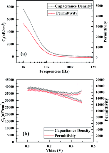 |
| | Fig. 7 (a) The frequency dependences of capacitance density (black curve) and permittivity (red curve), (b) the quasi-static Ci–V curve of the capacitor with the ITO/In0.0025Nb0.0025Ti0.995O2/ITO structure annealed at 400 °C for 30 minutes. | |
 |
| | Fig. 8 (a) The circuit of the inverter; (b) the input and output voltage of a resistor-loaded inverter with an In0.0025Nb0.0025Ti0.995O2/IZO TFT and a resistor (100 kΩ) at 500 Hz (VDD = 1.8 V). | |
Table 1 Comparison of different kinds of high dielectric constant gate insulator for TFTs
| Dielectric materials |
Dielectric types |
Ci (μF cm−2) |
Gate insulator thickness (nm) |
k |
SS (mV dec−1) |
Channel layer |
Mobility (cm2 V−1 s−1) |
Ref. |
Year |
| HfO2 |
High-k materials |
0.151 (100 Hz) |
104 |
18.5 |
∼180 |
ZnO |
40 |
1 |
2015 |
| PEO/LiClO4 |
Polymer electrolyte |
100 |
∼3000 |
∼3.4 × 10⁵ |
— |
P3HT |
0.7 |
9 |
2005 |
| DEME-TFSI |
Ionic liquid |
0.12 (0.01 Hz) |
∼10000 |
∼1350 |
100 |
ZnO |
— |
10 |
2009 |
| Mesoporous SiO2 |
Proton conduction |
1.7 (40 Hz) |
∼4000 |
∼7680 |
110 |
InGaZnO4 |
28.5 |
11 |
2009 |
| Ba0.7Sr0.3TiO3 |
Ferroelectrics |
0.261(40 Hz) |
670 |
∼200 |
260 |
Pentacene |
1.24 |
4 |
2012 |
| In0.0025Nb0.0025Ti0.995O2 |
Giant-dielectrics |
7.6 (1 kHz) |
380 |
3255 |
68 |
IZO |
1.88 |
This work |
2019 |
| 36.1 (quasi-static) |
15525 |
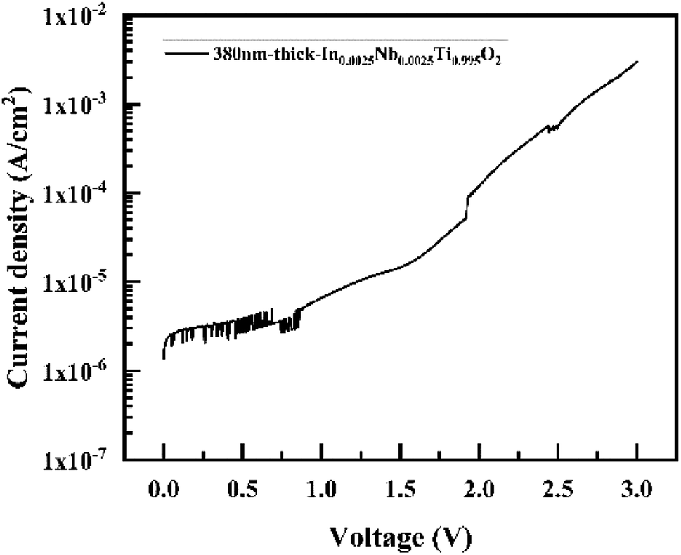
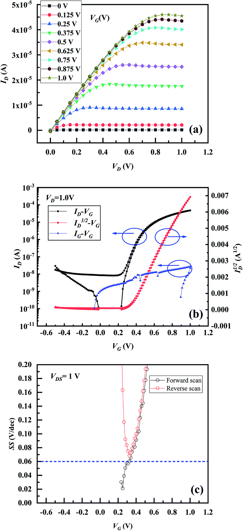
Fig. 9 shows the leakage current density versus voltage curve of the ITO/In0.0025Nb0.0025Ti0.995O2/ITO capacitor. The breakdown field was 64.2 kV cm−1. The relatively high leakage current might be attributed to the electron conduction in the crystalline grains. Fig. 10a and b show the output and the transfer characteristics (ID–VD curve and ID–VG curve) of the IZO-TFT with In0.0025Nb0.0025Ti0.995O2 gate dielectric, respectively. The operation voltage is only 1 V. No “current crowding” effects is observed at low drain voltage (VD) in the output curves, implying ohmic contacts between ITO S/D electrodes and IZO active layer. It is worth noting that there was not quadratic increase of saturation ID with increasing VG, which is because of space-charge polarization, in which some of the accumulated space charges will leak out at higher gate voltage (causing lowering of the permittivity). There was little hysteresis for the transfer curves between the forward and reverse sweeps (the measuring condition was presented in the ESI, see Fig. S2†), which was different from the TFTs with ferroelectric gate dielectrics. The threshold voltage (Vth) was 0.35 V. The mobility (μ) was calculated to be 1.88 cm2 V−1 s−1 using the quasi-static capacitance. The mobility and Vth distributions of the IZO-TFT with the In0.0025Nb0.0025Ti0.995O2 gate dielectric are shown in Fig. S1.† The average mobility of the devices was 1.94 cm2 V−1 s−1, and the maximum mobility was 2.21 cm2 V−1 s−1. The average Vth was 0.35 V. It is worth noting that the stability under gate bias stress was not good (the shift of Vth was −0.31 V under negative bias stress for 1 h, see Fig. S3†), which may be attributed to the defects at the interface between In0.0025Nb0.0025Ti0.995O2 and IZO.
 |
| | Fig. 9 The leakage current density versus voltage curve of the ITO/In0.0025Nb0.0025Ti0.995O2/ITO capacitor annealed at 400 °C for 30 minutes. | |
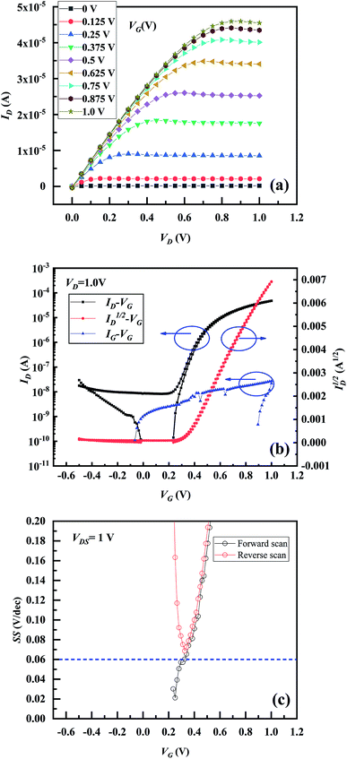 |
| | Fig. 10 (a) The output curve, (b) the transfer curve and (c) the SS–VG curve of the IZO-TFT with the In0.0025Nb0.0025Ti0.995O2 insulator. | |
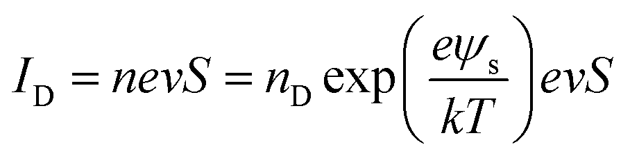
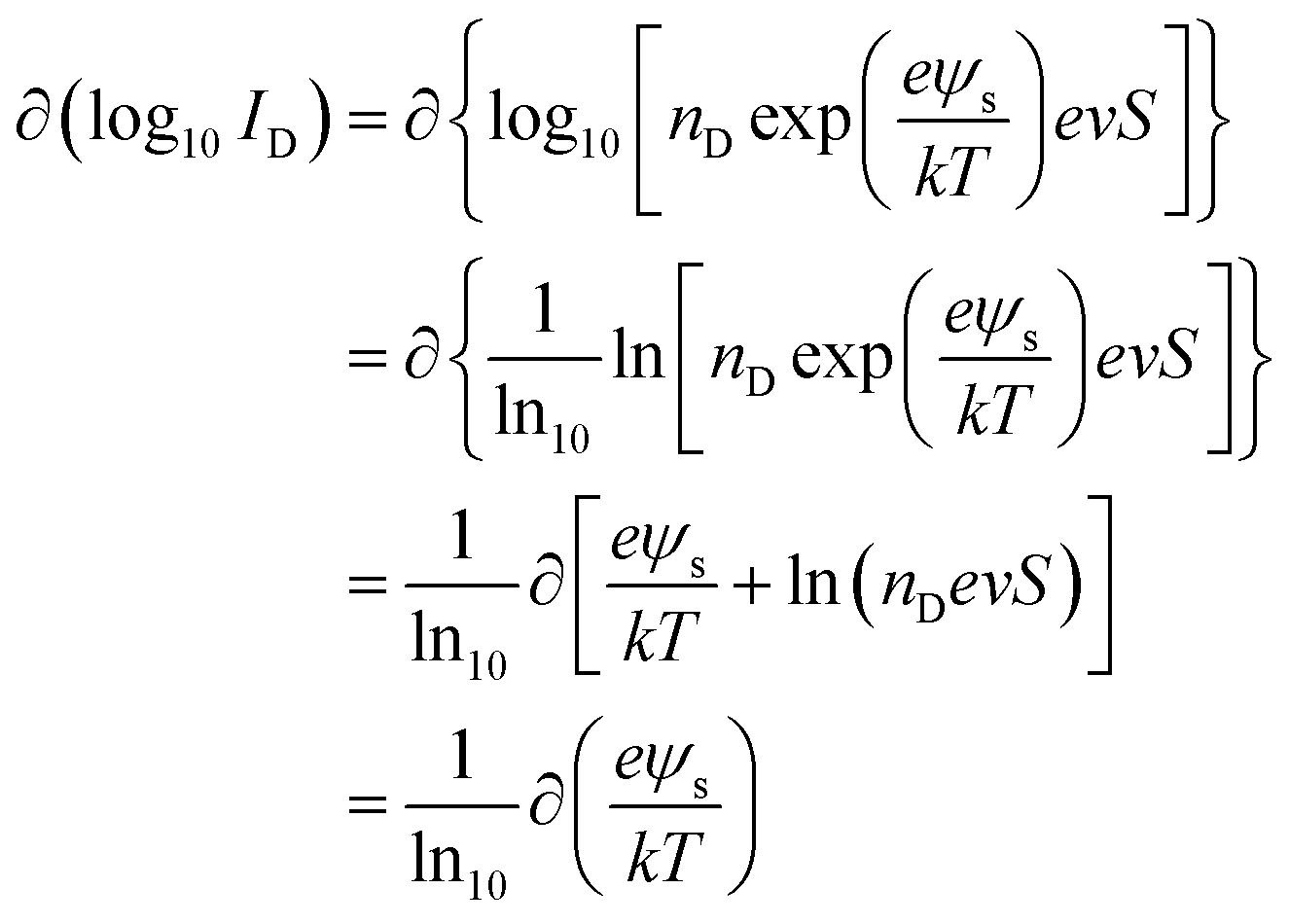
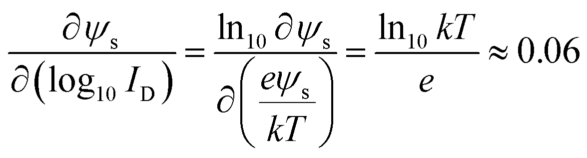
Fig. 10c shows the SS as a function of VG in the subthreshold regime. Theoretically, SS is expressed as,
| |
 | (2) |
where
Ψs is the surface potential of the semiconductor channel at the gate dielectric/semiconductor interface. ∂
VG/∂
Ψs given by
| |
 | (3) |
where
Cs is the capacitance of the semiconductor and
Cins is the capacitance of the gate dielectric, must exceed one (except for the negative capacitance). Because the carriers are confined into an ultrathin layer in close proximity to the gate dielectric/semiconductor interface, it is reasonable to assume that the carrier distribution within this ultrathin layer is uniform. Thus
ID can be expressed as
| |
 | (4) |
where
n is the carrier (electron) density at the interface,
e is the electron charge,
v is the electron velocity in the semiconductor,
S is the lateral area of the channel,
nD is the donor density,
k is Boltzmann constant, and
T is the absolute temperature. Thus,
| |
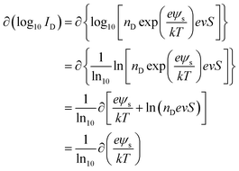 | (5) |
| |
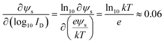 | (6) |
It can be deduced from eqn (2), (3) and (6) that SS should be greater than 0.06 V dec−1.26 For the IZO TFTs with In0.0025Nb0.0025Ti0.995O2 gate dielectrics, the gate leakage current of the forward sweep and much higher than that of the reverse sweep (see Fig. 10b), so the SS of the forward-sweep transfer curve was affected by the gate leakage current. For the reverse sweep of the transfer curve, the off current (Ioff) was much higher than the gate leakage current, so the SS of the reverse-sweep transfer curve was more accurate. It can be seen from Fig. 10c that the SS of the reverse-sweep transfer curve was about 0.068 V dec−1, very close to the lowest limit of the SS of the field-effect transistors (0.06 V dec−1). And the SS is the same as the IGZO-TFTs with ultrathin AlxOy gate dielectrics (∼3 nm).27 These results prove that the lowest limit of the SS (0.06 V dec−1) of the filed-effect transistors cannot be broken no matter how high the gate dielectric capacitance is (except for ferroelectric negative capacitors).
4. Conclusion
In conclusion, low-temperature (400 °C) giant-dielectric-constant thin films (In0.0025Nb0.0025Ti0.995O2) fabricated with simply radio frequency (RF) sputtering on glass substrates are employed as the gate dielectrics for thin-film transistors (TFTs) for the first time. The 380 nm-thick In0.0025Nb0.0025Ti0.995O2 film was in polycrystalline state with a quasi-static capacitance of as high as 36156 nF cm−2 with a quasi-static permittivity of 15525, and the capacitance was as high as 7607 nF cm−2 with a corresponding permittivity of 3266 at 1 kHz. Indium zinc oxide (IZO) TFTs with In0.0025Nb0.0025Ti0.995O2 gate dielectrics exhibited high output current (the mobility was 1.88 cm2 V−1 s−1, and the Vth was 0.35 V.) at low operation voltage (less than 1 V) and little hysteresis in the transfer curves between forward and reverse sweeps. The subthreshold swing (SS) of the IZO TFTs is 0.068 V dec−1, very close to the lowest limit of the SS of the field-effect transistors (0.06 V dec−1). The results also proves that the lowest limit of the SS (0.06 V dec−1) of the field-effect transistors cannot be broken no matter how high the gate dielectric capacitance is (except for negative capacitors). The TFTs demonstrate the potential for the application of low-power circuits and flat-panel displays.
Conflicts of interest
There are no conflicts to declare.
Acknowledgements
This work was supported by the National Key R&D Program (Grant No. 2016YFB0401105), the National Natural Science Foundation of China (Grant No. 51673068), the Guangdong Province Science and Technology Plan (Grant No. 2017A050503002 and 2016B090906002), the Guangdong Natural Science Foundation (Grant No. 2017A030306007), and the Fundamental Research Funds for the Central Universities.
Notes and references
- L. Zhou, M. Xu, X. Xia, J. Zou, L. Zhang, D. Luo, W. Wu, L. Wang and J. Peng, J. Disp. Technol., 2016, 12, 1064 CAS.
- M. Esro, G. Vourlias, C. Somerton, W. I. Milne and G. Adamopoulos, Adv. Funct. Mater., 2015, 25, 134 CrossRef CAS.
- J. M. Lee, I. T. Cho, J. H. Lee, W. S. Cheong, C. S. Hwang and H. I. Kwon, Appl. Phys. Lett., 2009, 94, 222112 CrossRef.
- J. H. Li, Z. H. Sun and F. Yan, Adv. Mater., 2012, 24, 88 CrossRef CAS.
- Z. R. Wang, J. Z. Xin, X. C. Ren, X. L. Wang, C. W. Leung, S. Q. Shi, A. Ruotolo and P. K. L. Chan, Org. Electron., 2012, 13, 1223 CrossRef CAS.
- Z. Zhao, V. Buscaglia, M. Viviani, M. T. Buscaglia, L. Mitoseriu, A. Testino, M. Nygren, M. Johnsson and P. Nanni, Phys. Rev. B Condens. Matter, 2004, 70, 024107 CrossRef.
- B. H. Hoerman, G. M. Ford, L. D. Kaufmann and B. W. Wessels, Appl. Phys. Lett., 1998, 73, 2248 CrossRef CAS.
- N. Uchida and T. Ikeda, Jpn. J. Appl. Phys., 1965, 4, 867 CrossRef CAS.
- S. Krupanidhi, N. Maffei, M. Sayer and K. El-Assal, J. Appl. Phys., 1983, 54, 6601 CrossRef CAS.
- M. J. Panzer and C. D. Frisbie, Adv. Funct. Mater., 2006, 16, 1051 CrossRef CAS.
- H. T. Yuan, H. Shimotani, A. Tsukazaki, A. Ohtomo, M. Kawasaki and Y. Iwasa, Adv. Funct. Mater., 2009, 19, 1046 CrossRef CAS.
- J. Jiang, Q. Wan, J. Sun and A. X. Lu, Appl. Phys. Lett., 2009, 95, 152114 CrossRef.
- A. P. Ramirez, M. A. Subramanian, M. Gardel, G. Blumberg, D. Li, T. Vogt and S. M. Shapiro, Solid State Commun., 2000, 115, 217 CrossRef CAS.
- M. A. Subramanian, D. Li, N. Duan, B. A. Reisner and A. W. Sleight, J. Solid State Chem., 2000, 151, 323 CrossRef CAS.
- B. S. Prakash and K. B. R. Varma, Phys. B, 2006, 382, 312 CrossRef CAS.
- J. B. Wu, C. W. Nan, Y. H. Lin and Y. Deng, Phys. Rev. Lett., 2002, 89, 217601 CrossRef PubMed.
- W. B. Hu, Y. Liu, R. L. Withers, T. J. Frankcombe, L. Noren, A. Snashall, M. Kitchin, P. Smith, B. Gong, H. Chen, J. Schiemer, F. Brink and J. Wong-Leung, Nat. Mater., 2013, 12, 821 CrossRef CAS PubMed.
- Z. G. Gai, Z. X. Cheng, X. L. Wang, L. L. Zhao, N. Yin, R. Abah, M. Zhao, F. Hong, Z. Y. Yu and S. X. Dou, J. Mater. Chem. C, 2014, 2, 6790 RSC.
- Y. Masuda and K. Kato, Chem. Mater., 2008, 20, 1057 CrossRef CAS.
- W. Song, L. F. Lan, P. Xiao, Z. G. Lin, S. Sun, Y. Z. Li, E. L. Song, P. X. Gao, P. Zhang, H. Xu, D. X. Luo, M. Xu and J. B. Peng, J. Phys. D: Appl. Phys., 2016, 49, 24LT01 CrossRef.
- E. J. Wang, W. S. Yang and Y. A. Cao, J. Phys. Chem. C, 2009, 113, 20912 CrossRef CAS.
- D. Morris, Y. Dou, J. Rebane, C. E. J. Mitchell, R. G. Egdell, D. S. L. Law, A. Vittadini and M. Casarin, Phys. Rev. B Condens. Matter, 2000, 61, 13445 CrossRef CAS.
- I. Ganesh, A. K. Gupta, P. P. Kumar, P. S. C. Sekhar, K. Radha, G. Padmanabham and G. Sundararajan, Mater. Chem. Phys., 2012, 135, 220 CrossRef CAS.
- E. Ramos-Moore, P. Ferrari, D. E. Diaz-Droguett, D. Lederman and J. T. Evans, J. Appl. Phys., 2012, 111, 014108 CrossRef.
- Y. L. Song, X. J. Wang, Y. Sui, Z. Y. Liu, Y. Zhang, H. S. Zhan, B. Q. Song, Z. G. Liu, Z. Lv, L. Tao and J. K. Tang, Sci. Rep., 2016, 6, 21478 CrossRef CAS PubMed.
- S. Salahuddin and S. Dattat, Nano Lett., 2008, 8, 405 CrossRef CAS PubMed.
- W. Cai, S. Park, J. Zhang, J. Wilson, Y. Li, Q. Xin, L. Majewski and A. Song, IEEE Electron Device Lett., 2018, 39, 375 CAS.
Footnote |
| † Electronic supplementary information (ESI) available: (1) Histograms of the (a) mobility and (b) threshold voltage of the IZO-TFT with the In0.0025Nb0.0025Ti0.995O2 gate dielectric. (2) The enlarge transfer curves of Fig. 10b. (3) The variations of time-dependent transfer curves of the IZO-TFT with the In0.0025Nb0.0025Ti0.995O2 insulator under negative gate bias stress. See DOI: 10.1039/c9ra03574e. |
|
| This journal is © The Royal Society of Chemistry 2019 |
Click here to see how this site uses Cookies. View our privacy policy here. 
 Open Access Article
 This Open Access Article is licensed under a Creative Commons Attribution-Non Commercial 3.0 Unported Licence
 * and
Junbiao Peng
* and
Junbiao Peng
 -related defects can be formed.17 However, no peaks related to Ti3+ was observed. It means that the giant dielectric behaviour of In0.0025Nb0.0025Ti0.995O2 was not due to the electron hoping between Ti4+ and Ti3+, which will be discussed later.