
 Open Access Article
 This Open Access Article is licensed under a Creative Commons Attribution-Non Commercial 3.0 Unported Licence
Chemical functionalization of the ZnO monolayer: structural and electronic properties
Lanli Chen ab,
Yuanyuan Cuib,
Zhihua Xiong*c,
Mingbin Zhouc and
Yanfeng Gao*b
ab,
Yuanyuan Cuib,
Zhihua Xiong*c,
Mingbin Zhouc and
Yanfeng Gao*b
aSchool of Mathematics and Physics, Hubei Polytechnic University, Huangshi 435003, China
bSchool of Materials Science and Engineering, Shanghai University, Shanghai 200444, China. E-mail: yfgao@shu.edu.cn
cKey Laboratory for Optoelectronics and Communication of Jiangxi Province, Jiangxi Science & Technology Normal University, Nanchang 330038, China. E-mail: xiong_zhihua@126.com
First published on 15th July 2019
Abstract
Two-dimensional zinc oxide (ZnO) materials have been extensively investigated both experimentally and theoretically due to their novel properties and promising applications in optoelectronic and spintronic devices; however, how to tune the electronic property of the ZnO monolayer is still a challenge. Herein, employing the first-principles calculations, we explored the effect of chemical functionalization on the structural and electronic properties of the ZnO monolayer. The results demonstrated that the hydrogenated-, fluorinated- or Janus-functionalized ZnO monolayers were thermodynamically and mechanically stable except for the fully hydrogenated ZnO monolayer. The band gap of the ZnO monolayer could be effectively modulated by hydrogenation or fluorination, which varied from 0 to 2.948 eV, as obtained by the PBE functional, and from 0 to 5.114 eV, as obtained by the HSE06 functional. In addition, a nonmagnetic metal → nonmagnetic semiconductor transition was achieved after hydrogenation, whereas a transition from a magnetic half-metal to nonmagnetic semiconductor occurred after fluorination of the ZnO monolayer. These results demonstrate that tunability of the electronic properties of the ZnO monolayer can be realized by chemical functionalization for future nanoelectronic device applications.
1. Introduction
Ever since graphene has been successfully fabricated in 2004, it has been widely used1 and thus has significantly promoted the development of other two-dimensional (2D) materials2–6 due to their intriguing properties and great potential in many important applications such as in field-effect transistors, nanoscale-electronic and spintronic devices, and optoelectronic devices.2–6The ZnO (zinc oxide) monolayer, as one of the representative 2D materials, possessing a graphene-analogous structure,7 has been theoretically predicted and experimentally synthesized on a Ag or Pd substrate.8,9 The pristine ZnO monolayer with the direct wide band gap of 3.4–4.0 eV exhibits the characteristics of a nonmagnetic semiconductor.10 However, its non-magnetism and improper band gap limit its applications in spintronic and optoelectronic devices. Thus, introducing magnetism and tailoring the band gap of the ZnO monolayer are valuable for both basic science and applications. Therefore, to significantly broaden the application scope of the ZnO monolayer, many attempts have been made such as element and hole doping,11,12 surface adsorption,13 and application of strain or an electric field.14,15 However, the question remains whether there are other routes to manipulate the electronic properties of 2D materials for their potential applications in nanoelectronics. Obviously, surface functionalization is an effective way to maintain the stability and reliability of devices to avoid rapid degradation caused by their reaction with oxygen under ambient conditions.16 Moreover, it has been reported that surface functionalization, such as hydrogenation and fluorination, can indeed tailor the electronic and magnetic properties of 2D materials.17–19 For example, complete hydrogenation and fluorination increased the record zero-bandgap of graphene and raised the band gap to 3.5 eV and 3.07 eV, respectively;18,20 recently, Shu et al.21 showed that hydrogenation and fluorination of the GaN monolayer not only solved the problem of instability, but also manipulated its bandgap from indirect to direct. Thus, the fundamental electronic and magnetic properties of the ZnO monolayer need to be further explored under surface functionalization.
Actually, the effect of chemical functionalization on the electronic and magnetic properties of ZnO has been previously studied. As early as 2010, Huang et al.22 have reported the results of the first-principles calculations, showing that the surface chemistry presents a strong effect on the electronic structures of ZnO nanowires, which is as significant as that of quantum confinement; moreover, they have found that full fluorination of ZnO nanowires leads to a decrease in their band gap. Chen et al.23 have reported that fluorination can also turn the nature of few-zinc oxide layers from semiconductor to half metallic with the half-metal gap of up to 0.56 eV and found that the F–ZnO ML has ferromagnetic coupling; in addition, Wang et al.24 have proposed that the half-metallic behavior exhibited by semi-fluorinated ZnO sheets is attributed to the decrease in the charge transfer from the Zn to the O atoms, and the nonmagnetic semiconductor behavior of the fully fluorinated ZnO sheets is due to their structural conformation. Experimentally, via selective surface molecular functionalization, the charge transport properties of ZnO nanowires could be affected depending on the polarity and orientation of molecules.25 Jayalakshmi et al.26 proposed a new approach to turn nonmagnetic ZnO into ferromagnetic ZnO via surface functionalization using thiol and amine due to the interaction between the adsorbates and the ZnO film and found that the oxygen vacancies were passivated upon surface functionalization; Han et al. reported that the electronic properties of the ZnO nanowires could be significantly tuned via surface modification for the application of these nanowires in field-effect transistors.27 In addition, the surface functionalization of ZnO nanoflakes with thiourea can enhance their sensitivity and selectivity, and the ZnO nanoflakes exhibit gas sensing characteristics, which pave the way for the realization of highly sensitive and selective fiber optic sensors.28 Trino et al.29 found that the functionalization of ZnO with four different organic bifunctional molecules not only could increase the corrosion resistance in ZnO, but could also lead to different wettabilities and surface energy behaviors.
All the abovementioned experimental and theoretical studies show that it is an interesting opportunity to achieve tunable electronic properties of the ZnO monolayer by surface functionalization. However, a systematic theoretical understanding of the electronic properties of the ZnO monolayer with half-, full-, and Janus-functionalization remains unclear. Therefore, it would be very interesting to further explore the structural and electronic properties of the ZnO monolayer by functionalizing it via hydrogenation or fluorination.
In this study, the possibilities of tuning the stability and electronic properties of the ZnO monolayer by chemical functionalization were extensively investigated based on the first-principles calculations. Our calculations revealed that surface functionalization could tune the band-gap of the ZnO monolayer; furthermore, the half-hydrogenated ZnO monolayer was found to be nonmagnetic metallic, whereas the half-fluorinated ZnO monolayer was found to be magnetic half-metallic. In addition, the hydrogenated-, fluorinated- and Janus-functionalized ZnO monolayers were thermodynamically and mechanically stable except for the fully hydrogenated ZnO monolayer. These studies provide guidance for future experiments and a deep understanding of the electronic properties of the ZnO monolayer, which are essential for ZnO-based optoelectronic devices.
2. Computational details
The Vienna ab initio simulation package (VASP) was employed to carry out the spin-polarized density functional theory (DFT) calculations, wherein the exchange correlation potentials within the Perdew–Burke–Ernzerhof (PBE) functional of the generalized gradient approximation (GGA) were chosen.30,31 The cutoff energy for the plane-wave basis was set as 450 eV. A 3 × 3 × 1 Monkhorst–Pack k-point grid in the Brillouin zone was sampled for structural optimization, and the 5 × 5 × 1 Monkhorst–Pack k-point grid was used for the density of states (DOS) calculations; to avoid coupling between neighboring slabs, the vacuum thickness was set as 15 Å along the z direction. The force and energy convergence criteria were set to be 0.02 eV Å−1 and 10−5 eV, respectively.The elastic constants32,33 of solids provide a detailed insight into the nature of the forces and mechanical behaviors of solids, and they also, in particular, provide information about the stability and stiffness of materials. While calculating the elastic constants of the chemically functionalized ZnO monolayer with a 4 × 4 × 1 supercell, we used a 450 eV energy cutoff and a 7 × 7 × 1 Monkhorst–Pack k-point mesh to converge the stress tensor. The force and energy convergence criteria were set to be 0.001 eV Å−1 and 10−5 eV, respectively.
The phonon frequencies of the pristine ZnO monolayer were calculated by the density functional perturbation theory at the force and energy convergence criteria of 0.0001 eV Å−1 and 10−8 eV, respectively.
Moreover, to more accurately predict the band gap of ZnO under chemical functionalization, the Heyd–Scuseria–Ernzerhof (HSE06) hybrid functional34 with the screening parameter of 0.2 Å−1 was used. In HSE06, a 2 × 2 × 1 supercell was adopted for structural relaxations. Moreover, a 5 × 5 × 1 Monkhorst–Pack k-point grid was used. The force and energy convergence criteria were set to be 0.001 eV Å−1 and 10−8 eV, respectively.
3. Results and discussion
3.1 Pristine ZnO monolayer
Table 1 presents the structural parameters of the relaxed ZnO monolayer with different chemical functionalizations. A 4 × 4 × 1 supercell (Zn16O16) of the pristine ZnO monolayer containing 32 atoms was constructed. Clearly, the Zn and O atoms are almost on the same plane with the buckled height of 0.002 Å (Δh = 0.002 Å), presenting a graphene-like flat plane for the pristine ZnO monolayer, as shown in Fig. 1(a). After structural optimization, the Zn–O bond length is 1.876 Å, which is 0.134 Å shorter than that in the pristine ZnO bulk (2.01 Å). These results are in agreement with the previous theoretical values of 1.80–1.90 Å (ref. 11–13) and the experimental value of 1.92 Å.8 As presented in Table 1, after structural relaxation, the Zn–O–Zn bond angle is 120°. These results show that the pristine ZnO monolayer exhibits sp2 hybridization of the Zn and O atoms. As shown in Fig. 1(b), the spin-up density of states are just symmetric with the spin-down density of states; this indicates that the pristine ZnO monolayer is actually a non-magnetic semiconductor; this agrees well with the previous theoretical results.11–13 Unless otherwise specified, when the density of states are greater than zero, the states are labeled as spin-up electronic states; however, when the density of states are less than zero, the states are labeled as spin-down electronic states. The non-magnetic behavior is attributed to the fact that each O atom receives sufficient electrons from the nearest Zn atoms to fill up all its p orbitals.23 Furthermore, the valence bands are mainly contributed by the O-2p and the Zn-3d states. In addition, as shown in Fig. 1(c), the conduction band minimum and the valence band maximum are at the same G point; this indicates that the ZnO monolayer is a direct bandgap semiconductor. Unless otherwise specified, the red lines with circles represent the spin-up bands, and the blue lines with square boxes represent the spin-down bands in the band structure diagram. The calculated band gap of the pristine ZnO monolayer (1.69 eV) is larger than that of the bulk ZnO (0.76 eV) obtained using the same method due to the existence of the quantum confinement effect, which is also consistent with the previous theoretical values of 1.66–1.96 eV for the ZnO monolayer.11,35,36 Fig. 1(d) shows the phonon spectra for the pristine ZnO monolayer. There is no imaginary frequency in the phonon spectra; this indicates that the pristine ZnO monolayer has good dynamic stability. This result is consistent with other calculated results.37| Configurations | Eb | ∠Zn–O–Zn | Δh | dZn–O | dF–Zn | dH–Zn | dF–O | dH–O |
|---|---|---|---|---|---|---|---|---|
| Pristine | — | 120 | 0.002 | 1.876 | — | — | — | — |
| Half-hydrogenated | 1.669 | 99.451 | 1.008 | 2.129 | — | — | — | 0.984 |
| Full-hydrogenated | 2.172 | 99.511 | 1.006 | 2.128 | — | 1.525 | — | 0.973 |
| Half-fluorinated | 1.876 | 107.403 | 0.738 | 2.016 | — | — | 2.130 | — |
| Full-fluorinated | 1.875 | 104.571 | 0.836 | 2.054 | 1.768 | — | 1.487 | — |
| Janus-functionalized | 3.098 | 101.251 | 0.948 | 2.102 | 1.763 | — | — | 0.974 |
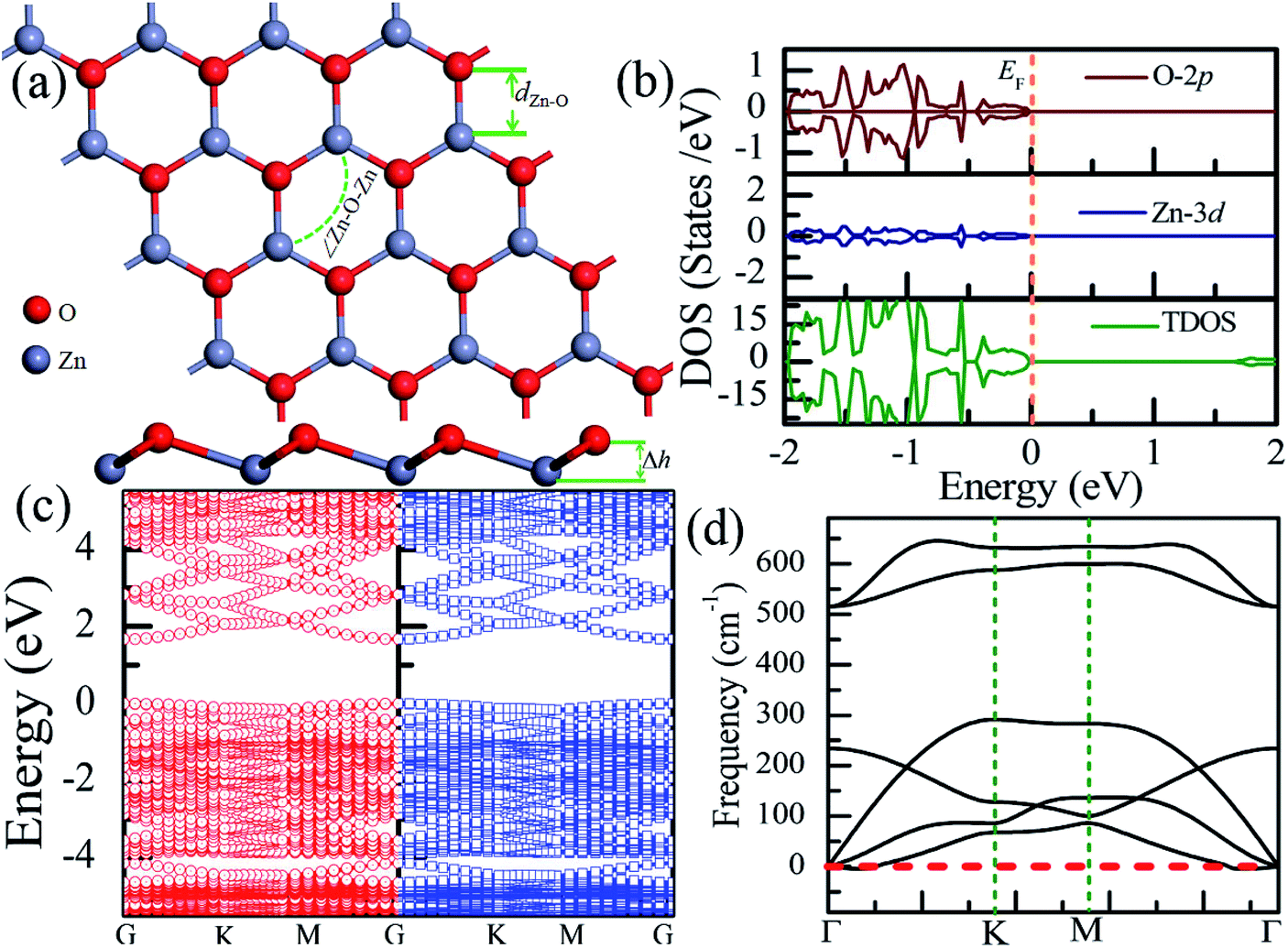 | ||
| Fig. 1 Calculated results for the pristine ZnO monolayer: (a) top and side views of the crystal structure, (b) DOS and PDOS, (c) band structures, and (d) phonon spectra. | ||
3.2 Hydrogen-functionalized ZnO monolayer
The total energy of the hydrogen atoms on the O atoms is more energetically favorable, which is comparatively lower than that on the Zn atoms. Thus, the stable configuration of the half-hydrogenated ZnO monolayer, as shown in Fig. 2(a), is that in which all the H atoms are bonded to the O atoms with the stoichiometric formula of Zn16O16H16. Specifically, the hydrogen atoms prefer to locate on top of the O atoms; this is consistent with the fact that the semi-hydrogenated atoms at the Zn sites are least stable.36 After structural optimization, the calculated Zn–O bond lengths in the half-hydrogenated ZnO monolayer increased to 2.129 Å, whereas the H–O bond length (0.984 Å) was similar to that of the typical H–O bond (0.98 Å); this was also consistent with the previous calculated values of 0.972–0.974 Å for the H–O bond length.36 These results indicate that strong chemical bonds are formed between the hydrogen atoms and the substrate. The calculated Zn–O–Zn bond angle is 99.451°, indicating that the interaction between the Zn and the O atoms changes from sp2 hybridization in the pristine ZnO to sp3 hybridization in the half-hydrogenated ZnO monolayer. As shown in Fig. 2(b), near the Fermi level, the energy bands ranging from −2.5 eV to 2.5 eV are mainly contributed by O-2p and slightly contributed by the H-1s orbital. Furthermore, the half-hydrogenated ZnO monolayer exhibits metallic properties as its Fermi level crosses the conduction band. Specifically, the conduction and valence bands overlap each other. The phenomenon of the metallization of the ZnO monolayer is attributed to its partially occupied surface state; actually, Tang et al. have found the same phenomenon that the ZnO sheets with semi-hydrogenated O sites exhibit a nonmagnetic metal state.36 As early in 2007, Jia et al.38 have also reported that the ZnO nanowires with partial dangling bonds of the side surface saturated by the H atoms are metallic. However, as compared to the case of the hydrogenated ZnO monolayer, graphene may turn the highly conductive zero-overlap semimetal into an insulator with dramatic changes in its transport properties.39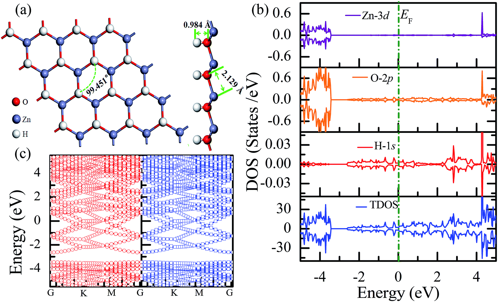 | ||
| Fig. 2 Calculated results for the half-hydrogenated ZnO monolayer: (a) top and side views of the crystal structure, (b) DOS and PDOS, and (c) band structures. | ||
Fig. 3(a) shows the relatively stable configuration for the fully hydrogenated ZnO monolayer (Zn16O16H32), in which 16 hydrogen atoms are bonded to 16 oxygen atoms on the O surface, and the other 16 hydrogen atoms are bonded to 16 Zn atoms on the Zn surface. After structural optimization, the H–Zn and H–O bond lengths became 1.525 Å and 0.973 Å, which indicated that the hydrogen atoms on top of the Zn atoms or O atoms formed strong Zn–H or O–H bonds; this was consistent with the previous calculated results for fully hydrogenated ZnO nanosheets (1.519 Å and 0.972 Å, respectively).36 Compared with those for the half-hydrogenated ZnO, the calculated Zn–O bond length (2.128 Å) and Zn–O–Zn bond angles (99.511°) for the fully hydrogenated ZnO monolayer exhibited no changes, also exhibiting the feature of sp3 hybridization. However, the electronic structure for the fully hydrogenated ZnO monolayer is quite different from that of the half-hydrogenated system. As shown in Fig. 3(b and c), the valence bands are attributed to a mixture of Zn-3d, O-2p and little H-1s orbitals. The spin-up and spin-down density of states are symmetric, demonstrating that the fully hydrogenated ZnO monolayer is a nonmagnetic semiconductor. Furthermore, the valence band maximum and the conduction band minimum are located at the M and G points, respectively, indicating that the fully hydrogenated ZnO monolayer is an indirect band gap semiconductor with the band gap of 1.732 eV, which is slightly higher than that of pristine ZnO (1.69 eV). This can be explained as follows: on the one hand, the H atoms are fully bonded to the Zn and O atoms, being saturated. On the other hand, the formation of the H–O or H–Zn bonds can stabilize the bonding molecular orbitals, push the antibonding molecular orbitals upward, remove the localized electronic states near the Fermi level, and thus increase the gap.22 In particular, a transition from a nonmagnetic metal to a nonmagnetic semiconductor can be achieved in the hydrogenated ZnO monolayer. Specifically, the ZnO monolayer with only O atoms saturated by the H atoms is metallic. In contrast, being completely saturated by the H atoms, the ZnO monolayer still exhibits a semiconductor behavior.
 | ||
| Fig. 3 Calculated results for the fully hydrogenated ZnO monolayer: (a) top and side views of the crystal structure, (b) DOS and PDOS, and (c) band structures. | ||
3.3 Fluorine-functionalized ZnO monolayer
Similar to the hydrogen-functionalized ZnO monolayer, the fluorine-functionalized ZnO monolayers, including half-fluorinated and fully fluorinated ZnO monolayers, were considered. As shown in Fig. 4(a), the relatively stable structure of the half-fluorinated ZnO monolayer is Zn16O16F16, where 16 fluorine atoms are bonded to 16 oxygen atoms on the oxygen surface. After geometric optimization, the F atoms are also on top of the O atoms, and the calculated F–O bond length is 2.130 Å, which is similar to the previously calculated value of 2.170 Å with the F atom located at the hollow site.23 The calculated Zn–O bond length is 2.016 Å, which is about 7.46% greater than that of the pristine ZnO. The Zn–O–Zn bond angle is 107.403°, which also displays the characteristic of sp3 hybridization. As shown in Fig. 4(b), the spin-up and spin-down densities of states for the half-fluorinated ZnO monolayer are asymmetric, exhibiting a magnetic behavior. Furthermore, the spin-down channel crosses the Fermi level, displaying the characteristic of a half-metal. In addition, the energy ranging from −4 to 0 eV is attributed to a mixture of the F-2p, O-2p and little Zn-3d orbitals, and the energy ranging from −5.5 to −4 eV is mainly dominated by Zn-3d and slightly dominated by the F-2p and O-2p orbitals. More interestingly, the 2p electrons of the O and F atoms are nearly the same in a short energy range near the Fermi level. Therefore, we can confirm that the magnetism with the total magnetic moment of 1.0 μB per formula for the half-fluorinated monolayer ZnO mainly originates from the O-2p and F-2p orbitals (as shown in Fig. 4(b)). This result is consistent with the other calculated results with the magnetic moment of 1 μB per unit in the F-center conformation.24 Moreover, Chen et al. have found that the total magnetic moment of the half-fluorinated ZnO ML is around 0.84 μB per unit cell.23 The spin-density distribution of the half-fluorinated ZnO monolayer is plotted in Fig. 5(a). It can be observed that the magnetism is mainly localized around the O atoms. The calculated magnetic moments of the O atoms and F atoms are 0.568 μB, and 0.295 μB, respectively. This phenomenon of magnetism can be explained as follows: the point group of the half-fluorinated ZnO monolayer is C3V. As shown in Fig. 5(b), there are six energy levels: 1a1, 1e, 2a1, 3a1, 2e, and 4a1. Because the O atom has six valence electrons and F atom has seven valence electrons, the fully occupied 1a1, 1e, 2a1, 3a1, and 2e levels are below the Fermi level, and the unoccupied 4a1 level is empty. According to the principle of minimum energy and Pauling's principle of non-tolerance, the electron occupation can be described as 1a1↑↓, 1e↑↓↑↓, 2a1↑↓, 3a1↑↓, and 2e↑↓↑, and thus, half-fluorination can result in the magnetic moment of 1 μB per unit cell in the ZnO monolayer. These results are also proven from the F-2p PDOS and its neighboring O-2p PDOS of the fluorinated ZnO monolayer, as shown in Fig. 5(c and d). Most states near the Fermi level mainly originate from the hybridization between the O-px and the O-py orbitals, and the others originate from the hybridization between the F-px and the F-py orbitals; as presented in Table 2, for the pristine monolayer, the O atoms receive electrons from the nearest Zn atoms, and the O-2p orbitals are filled and form pairs. Thus, the pristine ZnO exhibits a nonmagnetic behavior. However, compared with those in the pristine ZnO monolayer, the O-2p orbitals in the half-fluorinated ZnO monolayer are partially occupied and lead to half-metallicity. After half-fluorination, the electrons will transfer from the Zn atoms to the F atoms, and thus, the electrons in the O atoms will be unpaired. Therefore, half-fluorination produces the total magnetic moment of 1.0 μB per formula. As shown in Fig. 4(c), the majority of spin states open the band gap of 2.929 eV, exhibiting semiconducting characteristics. However, the minority spin states have densities up to 0.60 eV above the Fermi level, presenting a metallic state.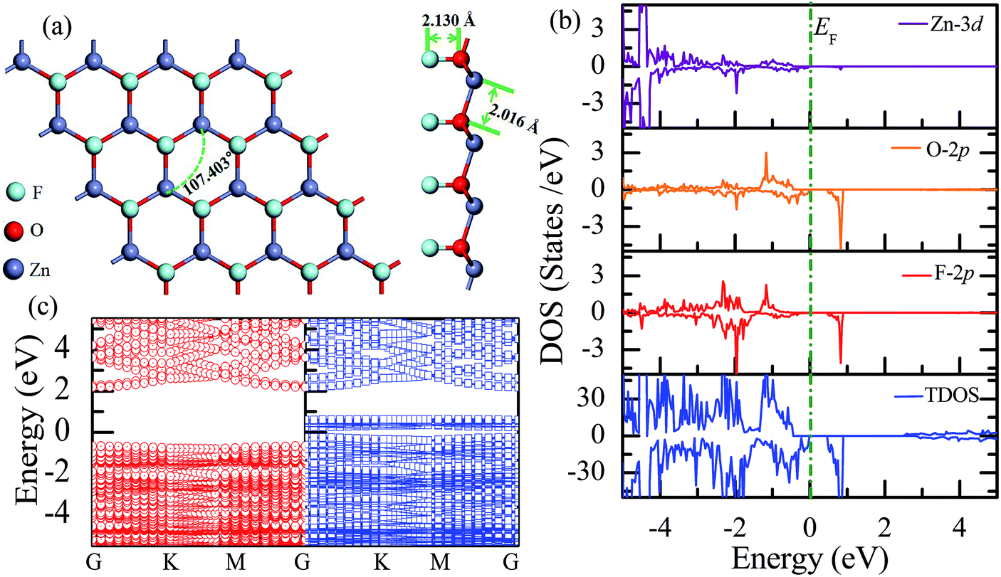 | ||
| Fig. 4 Calculated results for the half-fluorinated ZnO monolayer: (a) top and side views of the crystal structure, (b) DOS and PDOS, and (c) band structures. | ||
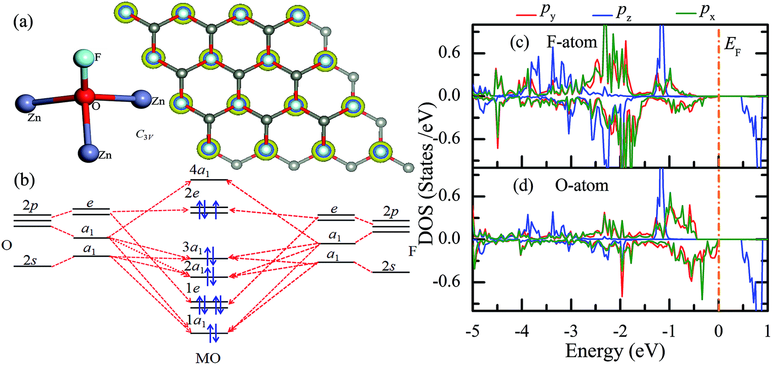 | ||
| Fig. 5 (a) Spin-density distribution, (b) schematic of molecular orbitals (MO), (c) spin-polarized F's 2p PDOS, and (d) neighboring O's 2p PDOS for the half-fluorinated ZnO monolayer. The Fermi level is aligned to zero. The isosurface value for the spin charge is 0.0098159 e Å−3. | ||
| Configuration | O | Zn | F1 | F2 | H1 | H2 |
|---|---|---|---|---|---|---|
| Pristine | 7.227 | 10.773 | — | — | — | — |
| Half-hydrogenated | 7.263 | 11.297 | — | — | 0.440 | — |
| Full-hydrogenated | 7.267 | 11.096 | — | — | 0.411 | 1.225 |
| Half-fluorinated | 6.786 | 10.654 | 7.560 | — | — | — |
| Full-fluorinated | 6.496 | 10.740 | 7.545 | 7.219 | — | — |
| Janus-functionalized | 7.286 | 10.720 | 7.623 | — | 0.373 | — |
Subsequently, we have explored the structural and electronic properties of the fully fluorinated ZnO monolayer (Zn16O16F32), wherein 16 F atoms are bonded to 16 O atoms on the O surface, and the other 16 F atoms are bonded to 16 Zn atoms on the Zn surface. Although there are four possible configurations of the fully fluorinated ZnO monolayers, i.e. the hill, chair, boat and twist-chair configurations,24 their energy difference obtained employing the PBE potential is only about 0.2 eV. Therefore, herein, we only considered the chair configuration since it is similar to fluorinated-graphene.18 As shown in Fig. 6(a), the calculated F–Zn and F–O bond lengths are 1.768 Å and 1.487 Å, respectively. In addition, the bond lengths of Zn–O are increased to 2.054 Å after full fluorination, being similar to that of the wurtzite bulk ZnO system (2.01 Å). The calculated Zn–O–Zn bond angle is 104.571°. These results further confirm that the hybridization transformation is still from sp2 to sp3 after full fluorination. Interestingly, unlike the case of the half-fluorinated ZnO monolayer, the spin-up and spin-down density of states are totally symmetric in the case of the fully fluorinated ZnO monolayer; this indicates that the fully fluorinated ZnO monolayer exhibits a nonmagnetic behavior, as shown in Fig. 6(b). Furthermore, its valence bands are mainly contributed by the O-2p and Zn-3d states, whereas the conduction bands within the range of 0.5–2.0 eV are mainly composed by the O-2p and F-2p states, and the contributions from the O atoms are negligible. In addition, as shown in Fig. 6(c), the calculated direct band gap for the fully fluorinated ZnO monolayer as low as 2.948 eV is larger than that of the pristine ZnO monolayer, which is attributed to the formation of localized states induced by the paired O-2p states (as shown in Fig. 5(b)). This result also agrees with the fact that 100% F passivation of the surfaces of ZnO nanowires leads to a decrease in their band gap.22 Compared to the case of the hydrogenated-ZnO monolayer, a transition from the magnetic half-metal behavior to the nonmagnetic semiconductor behavior can be observed in the fluorinated ZnO monolayer.
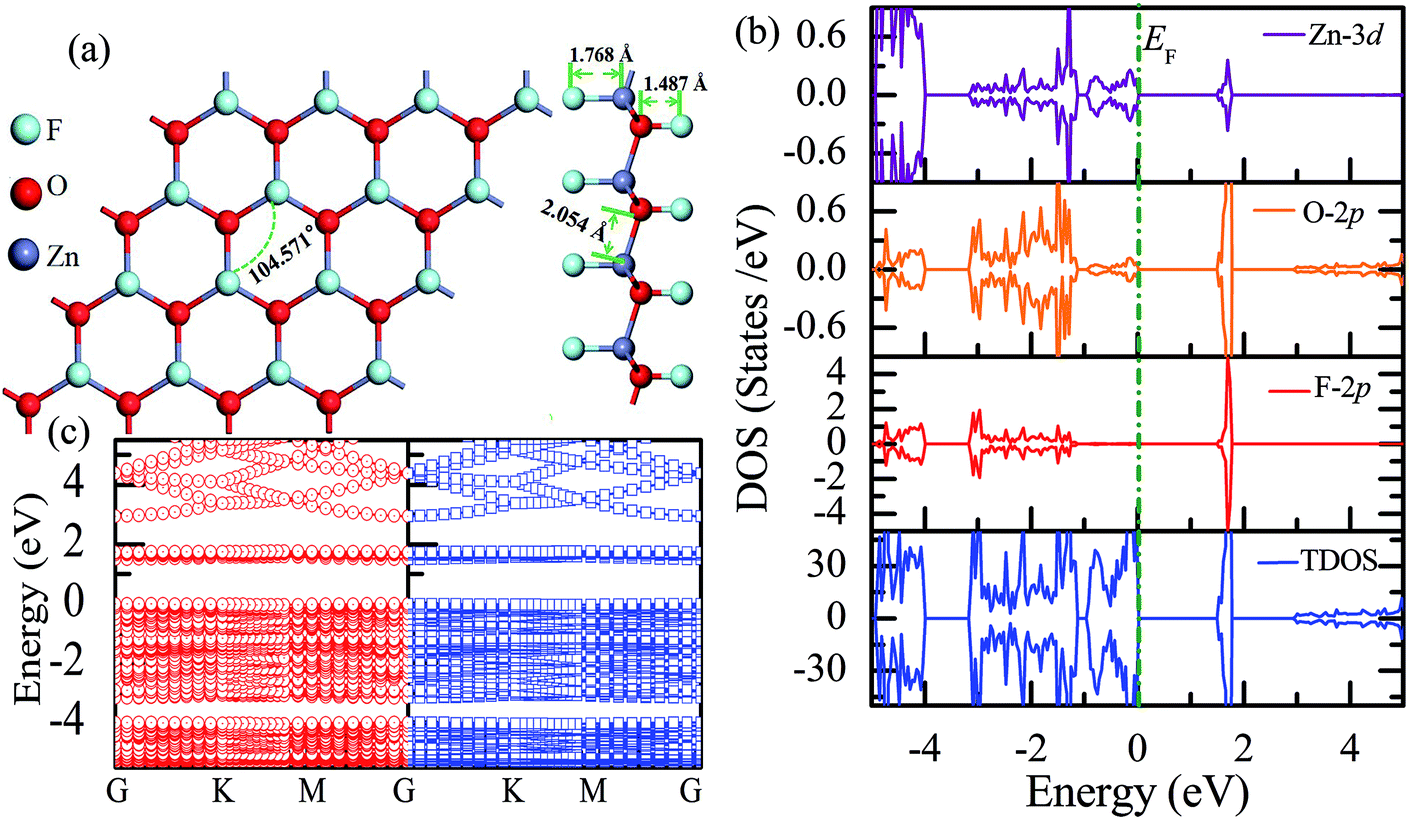 | ||
| Fig. 6 Calculated results for the fully fluorinated ZnO monolayer: (a) top and side views of the crystal structure, (b) DOS and PDOS, and (c) band structures. | ||
3.4 Janus-functionalized ZnO monolayer
Recently, 2D Janus materials in the form of ultra-thin films have received extensive attention.18,40 For example, Sofo et al.18 have predicted that graphene possess a fully saturated hydrocarbon structure constructed by the bonding H atoms on both sides of a single graphene layer that leads to the band gap widening of 3.5–3.7 eV. Ng et al.40 also reported that the combined hydrogenation and halogenation on graphene could realize band structure engineering possibilities.40 Sun et al.41 found that the band gap of Janus silicene could vary from 1.91 to 2.66 eV by tuning the chemical composition of the adatoms. Actually, half-functionalization could be obtained experimentally by applying an external electric field perpendicular to the fully functionalized monolayer.39 Following the idea of Janus-graphene, herein, we studied the Janus-functionalized ZnO monolayer with the H and F atoms; this monolayer was constructed in a way such that its one side was hydrogenated and the other side was fluorinated; hereinafter, this monolayer has been referred to as the Janus-functionalized ZnO monolayer. For the Janus-functionalized ZnO monolayer, a relatively stable structure (Zn16O16F16H16) is that in which 16 H atoms are bonded to 16 O atoms and 16 F atoms are bonded to 16 Zn atoms. The relaxed atomic configuration of the Janus-functionalized ZnO monolayer from the top and side views is shown in Fig. 7(a). As reported by Huang et al., the structural transformation is related to the electronegativity of elements.22 For example, the electronegativity of O (3.44) is lower than that of F (3.98) and larger than that of H (2.20), the F atoms on top of the Zn atoms may obtain more electrons from the Zn atoms, and the H atoms may obtain some electrons from the O atoms. Thus, the strength of F bonded to Zn is larger than that of F bonded to O, and the strength of H bonded to Zn is smaller than that of H bonded to O; thus, the Janus-functionalized ZnO monolayer is formed. After structural optimization, as shown in Fig. 7(a), the calculated Zn–O bond length is 2.102 Å. The calculated H–O and F–Zn bond lengths are 0.974 Å, and 1.763 Å, respectively, indicating strong chemical bonds. The Zn–O–Zn bond angle is 101.251°. These results indicate that the Zn and O atoms are in sp3 hybridization with the H atoms and the F atoms. As shown in Fig. 7(b), the spin-up and spin-down densities of states are totally symmetric; this indicates that the Janus-functionalized ZnO monolayer maintains the non-magnetic states. The valence band near the Fermi level is mainly dominated by the F-2p and Zn-3d orbitals and slightly dominated by the O-2p orbital. Moreover, the F-2p orbitals become fully occupied. The Bader analysis shows that the full occupancy originates from the charge transfer from the Zn to the F atoms after Janus-functionalization. Interestingly, the Janus-functionalized ZnO monolayer is still a semiconductor material but with the direct band gap of 0.958 eV (as shown in Fig. 7(c)).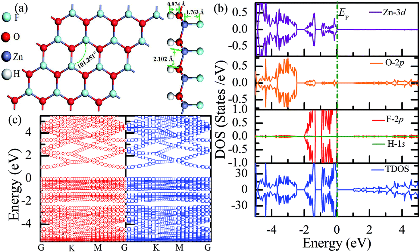 | ||
| Fig. 7 Calculated results for the Janus-functionalized ZnO monolayer: (a) top and side views of the crystal structure, (b) DOS and PDOS, and (c) band structures. | ||
3.5 Discussion
As shown in Fig. 8(a), after chemical functionalization, along the z direction, the Zn atoms relax inward, whereas the O atoms relax outward, and thus, significant buckling is formed. For example, the optimized structure of the Janus-functionalized ZnO monolayer is buckled with the buckling height (Δh) of 0.948 Å between Zn–O atoms, which is higher than that of the fluorinated-functionalized monolayer (0.738 Å and 0.836 Å for the half-fluorinated and fully fluorinated monolayers, respectively), but lower than that of the hydrogenated-functionalized monolayer (1.008 Å and 1.006 Å for the half-hydrogenated and fully hydrogenated, respectively). These phenomena are in close accordance with the previous results obtained for ZnO nanowires.22,24 Chemical functionalization can induce an increase in the buckling height (Δh) between Zn and O in the ZnO monolayer; this is due to the formation of H–O and F–Zn bonds. Furthermore, it was found that the planar sp2 hybrid orbitals changed to sp3-like orbitals after chemical functionalization. In addition, high Δh induces strong anisotropy.42 These results can be explained from the charge distributions and charge transfer. As shown in Table 2, for the pristine ZnO monolayer, the Zn and O atoms gain or lose the charges of about 1.227e (12e − 10.773e = 1.227e) and −1.227e (6e − 7.227e = −1.227e), respectively; this indicates that the Zn–O rings weakly affect the charge distribution on the Zn and O atoms.22 However, a certain amount of charge is transferred from the ZnO monolayer to the H or F atoms after chemical functionalization, which will induce notable buckling in the ZnO monolayer. | ||
| Fig. 8 Calculated results for the ZnO monolayer with different functionalizations. (a) Buckled height (Δh), (b) band gaps by PBE and HSE06 potential, (c) electrostatic potential along the z direction, and (d) binding energy (Eb) and the adsorption energy (Eads). | ||
To obtain a more accurate prediction of the band gaps of chemically functionalized ZnO monolayer, the HSE06 functional calculations were employed. Considering our limited computational resources, the 2 × 2 × 1 supercells were employed. Fig. 9 and 10 show the band gaps of the pristine and chemically functionalized ZnO monolayer with the HSE06 functional. It has been found that the pristine ZnO monolayer is a semiconductor with the direct band gap of 3.374 eV, which is consistent with the experimental result of about 3.4 eV. As is well-known, the band gap is also very sensitive to chemical functionalization. As shown in Fig. 9 and 10, the band gaps with the HSE06 functional for the half-fluorinated, Janus-functionalized and fully fluorinated ZnO monolayer are 5.114 eV, 2.523 eV, and 3.322 eV, respectively. In contrast, the corresponding band gaps obtained from the PBE functional are 2.929 eV, 0.958 eV, and 2.948 eV. It has been found that the variation trend in the band gap of the pristine and chemically functionalized ZnO monolayer is the same as observed using the PBE and HSE06 functionals (as shown in Fig. 8(b)). After chemical functionalization, the configurations except for the half-functionalized configuration still maintained the semiconductor state. Furthermore, it has been found that the band gap of the ZnO monolayer increases with the coverage of hydrogen, whereas it is just the opposite for the fluorinated ZnO monolayer. On the one hand, the variable band gap after chemical functionalization is attributed to the hybridization transformation from sp2 to sp3, which is supported by the structural information, as displayed in Section 3.1–3.4. On the other hand, the reason may be due to the stronger electronegativity of fluorine than that of hydrogen. The currents results indicate that the surface-functionalized ZnO monolayer is ideal for applications in nanoelectronics.
 | ||
| Fig. 9 Band structures of the ZnO monolayer obtained by the HSE06 functional. (a) Pristine, (b) half-hydrogenated, and (c) fully hydrogenated. The red lines represent the spin-up bands, whereas the black lines represent the spin-down bands. | ||
 | ||
| Fig. 10 Band structures of the ZnO monolayer obtained by the HSE06 functional. (a) Half-fluorinated, (b) fully fluorinated, and (c) Janus-functionalized. The red lines represent the spin-up bands, whereas the black lines represent the spin-down bands. | ||
Fig. 8(c) shows a shift in the vacuum level when the Fermi level is aligned manually. The calculated work function of the pristine ZnO monolayer is 5.08 eV, which is higher than our previous theoretical result (4.574 eV) based on DFT + U. However, the result is closer to the experimental work function of the ZnO surface in the range of 5.4–6.5 eV.43 Compared with the case of the pristine ZnO monolayer, surface functionalization leads to an increase in the work function except for the half-hydrogenated monolayer. We could tune the work function of the ZnO monolayer by 2 eV after fluorinated-functionalization. For example, the work function after Janus-functionalization could be increased by an additional 1.96 eV when compared with the case of the pristine monolayer. This phenomenon may be attributed to the changes in the electron behavior in the surface-functionalized ZnO monolayer.
Next, the magnetic properties of the chemically functionalized ZnO monolayer have been discussed. Why the half-fluorinated ZnO is spin-polarized, whereas the half-hydrogenated ZnO monolayer is nonmagnetic? As discussed in Section 3.2, the electron states in the half-hydrogenated monolayer at the Fermi level mainly originate from the contribution by the O-2p and little H-1s valence orbitals. There are abundant localized surface states near the Fermi level, which will induce the metallization of the ZnO monolayer. Furthermore, the dangling bonds on the Zn atoms exhibit much less spin density. However, for the half-fluorinated ZnO monolayer, the electron states near the Fermi level mainly originate from the contribution by the O-2p and F-2p valence orbitals. The dangling bonds will remove the localized surface states from the band-gap region. On the other hand, because the electronegativity of O (3.44) is lower than that of F (3.98) but higher than that of H (2.20), the F atoms on the F–O bonds increase the charge of O, whereas the H on the H–O bonds reduce the charge of O. Thus, the charge of F bonded to O is larger than that of H bonded to O. These results can also be proven by the atomic charges obtained via the Bader charge analysis. For the hydrogenated ZnO monolayer, each O atom receives enough electrons from the nearest H atoms to fill up all the p orbitals, and thus, the hydrogenated ZnO monolayer exhibits a non-magnetic state. However, for the fluorinated ZnO monolayer, about one electron transfers from a Zn to a F atom, leaving an electron in the O atoms unpaired, and thus, magnetic moment in the half-fluorinated ZnO monolayer is produced.
Finally, we have discussed the stability of the ZnO monolayer with chemical functionalization from the point of view of energy and mechanical parameters. The binding energy Eb of the ZnO monolayer with chemical functionalization is defined by Eb = (Epristine + nEatom − Etot)/n, where Epristine, Eatom, and Etot represent the total energies of the pristine ZnO monolayer, isolated H/F atom, and the systems with surface functionalization. The higher binding energy shows surface functionalized occurs easily. As shown in Fig. 8(d), it is found that the ZnO monolayer with surface functionalization is thermodynamically stable and possible to obtain. More interestingly, the binding energy of the Janus-functionalized ZnO monolayer is the highest in all the considered cases, indicating that the Janus-functionalized ZnO monolayer is the most stable and can be realized in experiment. Therefore, we can conclude that it is an easy way to achieve Janus-functionalized ZnO monolayers in experiments. To further discuss the structural stability of the chemically functionalized ZnO monolayer, here, we calculated the adsorption energy (Eads) of all the considered cases. The adsorption energy (Eads)13 is calculated by Eads = (Echemical-functionalized − Epristine − nμH/F)/n, where Echemical-functionalized is the total energy of the chemically functionalized ZnO monolayer, Epristine is the total energy of the pristine ZnO monolayer, and μH/F is the chemical potential the H or F atom in its reference phase (calculated with respect to the gas in nature). As shown in Fig. 8(d), the adsorption energies of the ZnO monolayer are all negative, indicating that hydrogenation and fluorination on the ZnO monolayer are more energetically stable. Fig. 11 shows the phonon spectra for the chemically functionalized ZnO monolayer. Phonon softening instabilities were obtained from the DFT calculations, which imply that the chemically functionalized ZnO monolayer is not a stable structure. These results are expected because chemical functionalization is stable only under typical growth/synthesis conditions. It is well-known that the chemical vapor deposition of ZnO thin films is generally completed at temperatures above 700 °C. For example, the ZnO nanowires were found to grow downstream at a temperature of approximately 700 °C on horizontally positioned alumina substrates.25
 | ||
| Fig. 11 Phonon spectra for the chemically functionalized ZnO monolayer. (a) Half-hydrogenated, (b) fully hydrogenated, (c) half-fluorinated, (d) fully fluorinated, and (e) Janus-functionalized. | ||
To further examine their stability, we analyzed the mechanical stability of the pristine and chemically functionalized ZnO monolayers by calculating their linear elastic constants. The elastic constants of the chemically functionalized ZnO monolayer are listed in Table 3. According to ref. 44, the mechanical stability criteria are given by the relationship: C44 > 0, C11 > |C12|, and (C11 + C22)C33 > 2C132. It can be found that the ZnO monolayers with surface functionalization are mechanically stable except the fully hydrogenated monolayers. Interestingly, using the same criterion method, fully-fluorinated borophene was also found to be unstable, while the half-fluorinated borophene was shown to be dynamically stable.45 In addition, it is well-known that the value of Bv/Gv can reflect the brittleness of a material.46 A high value of Bv/Gv is associated with malleability and a low value with brittleness. According to the equations: Bv = (1/9)[2(C11 + C12) + 4C13 + C33], Gv = (1/30)(M + 12C44 + 12C66), and M = C11 + C12 + 2C33 − 4C13, Bv, Gv, and Bv/Gv were calculated. As shown in Table 2, the Bv/Gv for the half-hydrogenated ZnO monolayer is much larger than others, indicating that the ZnO monolayer with half-hydrogenation is malleable. However, the Bv/Gv for the fully hydrogenated ZnO monolayer is negative, further proving that the fully hydrogenated ZnO monolayer is mechanically unstable. The other systems are relative mechanically stable. In addition, the in-plane Young's modulus Y and Poisson's ratio ν were calculated using the following relationship:47 Y = (C112 − C122)/C11 and ν = C12/C11, respectively. The Poisson's ratio reflects the stability of the crystal against shear. As shown in Fig. 12(a), it has been found that the Young's moduli of the fully fluorinated and hydrogenated ZnO monolayer are smaller than that of the pristine ZnO monolayer, showing that the fully fluorinated and hydrogenated ZnO monolayer have good flexibility. In addition, as shown in Fig. 12(b), after fluorination or hydrogenation of the ZnO monolayer, the Poisson's ratio decreases in the range from 0.19 to 0.42, which is lower than that of the pristine ZnO monolayer with the value of 0.7. Therefore, surface functionalization by the H and F atoms serves as an important approach for tailoring the electronic properties of the ZnO monolayer. However, the theoretical calculation results need to be further verified experimentally.
| Configuration | C44 | C11 | C12 | C33 | C13 | C22 | C55 | C66 | Bv | Gv | Bv/Gv |
|---|---|---|---|---|---|---|---|---|---|---|---|
| Pristine | 14.13 | 95.84 | 66.65 | 6.3 | 1.67 | 94.38 | 0.54 | 1.04 | 37.55 | 11.69 | 3.21 |
| Half-hydrogenated | 0.3 | 4.26 | 0.80 | −19.37 | −15.69 | −4.07 | −18.74 | −4.71 | −8.00 | −0.80 | 10.00 |
| Full-hydrogenated | −14.52 | 15.48 | 29.1 | 5.24 | 1.20 | 7.8 | −16.83 | −4.67 | 11.37 | −6.11 | −1.86 |
| Half-fluorinated | 21.80 | 68.12 | 26.51 | 12.35 | 3.86 | 72.03 | −1.61 | −1.83 | 24.11 | 11.45 | 2.11 |
| Full-fluorinated | 13.58 | 37.64 | 9.45 | 11.90 | −3.68 | 60.56 | −4.07 | −9.6 | 10.16 | 4.44 | 2.29 |
| Janus-functionalized | 12.84 | 41.91 | 17.69 | 8.30 | 1.73 | 44.96 | −24.15 | −12 | 14.93 | 3.11 | 4.81 |
 | ||
| Fig. 12 Calculated Young's modulus (a) and Poisson's ratio (b) of the relatively stable configurations for the chemically functionalized ZnO monolayer. | ||
4. Concluding remarks
In summary, the behaviors of the hydrogenated and fluorinated ZnO monolayers and the influence of hydrogenation and fluorination on the structural and electronic properties of the ZnO monolayer were investigated using the first-principles calculations. The results indicate that the hydrogenated and fluorinated ZnO monolayers, except for the fully hydrogenated ZnO monolayer, are energetically and mechanically stable. The hydrogenated or fluorinated ZnO monolayers exhibit a semiconductor behavior with band gaps in the range of 0–2.948 eV by the PBE functional and from 0 to 5.114 eV by the HSE06 functional except for the half-hydrogenated ZnO monolayer. In addition, a transition from the nonmagnetic metal to nonmagnetic semiconductor can be achieved after hydrogenation. However, a magnetic half-metal → nonmagnetic semiconductor transition occurs after fluorination. The current findings show that the possibility of tuning the structural and electronic properties via surface functionalization opens a door to the applications of ZnO-based materials in electronic and optoelectronic devices.Conflicts of interest
There are no conflicts to declare.Acknowledgements
The authors gratefully acknowledge the support received from the National Natural Science Foundation of China (61764006, 61564004, 51572167, 51402182 and 51372228), the Open Project Fund of Key Laboratory for Optoelectronics and Communication of Jiangxi Province (20181OEC001), and School-level Scientific Research Project of Hubei Polytechnic University (18xjz11R).References
- K. S. Novoselov, A. K. Geim, S. V. Morozov, D. Jiang, Y. Zhang, S. V. Dubonos, I. V. Grigorieva and A. A. Firsov, Science, 2004, 306, 666–669 CrossRef CAS.
- B. Radisavljevic, A. Radenovic, J. Brivio, V. Giacometti and A. Kis, Nat. Nanotechnol., 2011, 6, 147–150 CrossRef CAS PubMed.
- P. Vogt, P. Padava, C. Quaresima, J. Avila, E. Frantzeskakis, M. Asensio, A. Resta, B. Ealet and G. Lay, Phys. Rev. Lett., 2012, 108, 155501 CrossRef.
- N. Tombros, C. Jozsa, M. Popinciuc, H. T. Jonkman and B. J. v. Wees, Nature, 2007, 448, 571 CrossRef CAS.
- A. Ismach, H. Chou, D. Ferrer, Y. Wu, S. McDonnell, H. Floresca, A. Covacevich, C. Pope, R. Piner, M. Kim, R. Wallace, L. Colombo and R. Ruoff, ACS Nano, 2012, 6, 6378–6385 CrossRef CAS.
- L. Li, Y. Yu, G. Ye, Q. Ge, X. Ou, H. Wu, D. Feng, X. Chen and Y. Zhang, Nat. Nanotechnol., 2014, 9, 372–377 CrossRef CAS.
- Q. Yao, Y. Liu, R. Lu, C. Xiao, K. Deng and E. Kan, RSC Adv., 2014, 4, 17478–17482 RSC.
- C. Tusche, H. Meyerheim and J. Kirschner, Phys. Rev. Lett., 2007, 99, 026102 CrossRef CAS.
- G. Weirum, G. Barcaro, A. Fortunellli, F. Weber, R. Schennach, S. Surnev and F. Netzer, J. Phys. Chem. C, 2010, 114, 15432–15439 CrossRef CAS.
- H. Hong, J. Jo, D. Hwang, J. Lee, S. Son, J. Kim, M. Jin, Y. Jun, R. Erni, S. Kwak, J. Yoo and Z. Lee, Nano Lett., 2017, 17, 120–127 CrossRef CAS.
- H. Guo, Y. Zhao, N. Lu, E. Kan, X. Zeng, X. Wu and J. Yang, J. Phys. Chem. C, 2012, 116, 11336–11342 CrossRef CAS.
- L. Chen, A. Wang, Z. Xiong, S. Shi and Y. Gao, Appl. Surf. Sci., 2019, 467–468, 22–29 CrossRef CAS.
- L. Chen, S. Li, Y. Cui, Z. Xiong, H. Luo and Y. Gao, Appl. Surf. Sci., 2019, 479, 440–448 CrossRef CAS.
- B. Rakshit and P. Mahadevan, Appl. Phys. Lett., 2013, 102, 143116 CrossRef.
- B. Bahuguna, L. Saini, R. Sharma and B. Tiwari, Phys. E, 2018, 99, 236–243 CrossRef CAS.
- Y. IIIarionov, M. Waltl, G. Rzepa, J. Kim, S. Kim, A. Dodabalapur, D. Akinwande and T. Grasser, ACS Nano, 2016, 10, 9543–9549 CrossRef PubMed.
- S. Zhang, Y. Hu, Z. Hu, B. Cai and H. Zeng, Appl. Phys. Lett., 2015, 107, 022102 CrossRef.
- J. Sofo, A. Chaudhari and G. Barber, Phys. Rev. B: Condens. Matter Mater. Phys., 2007, 75, 153401 CrossRef.
- A. Peyghan and M. Noei, J. Mol. Model., 2013, 19, 3941–3946 CrossRef CAS.
- J. Robinson, J. Burgess, C. Junkermeier, S. Badescu, T. Reinecke, F. Perkins, M. Zalalutdniov, J. Baldwin, J. Culbertson, P. Sheehan and E. Snow, Nano Lett., 2010, 10, 3001–3005 CrossRef CAS.
- H. Shu, X. Niu, X. Ding and Y. Wang, Appl. Surf. Sci., 2019, 479, 475–481 CrossRef CAS.
- S. Huang, H. Xu, I. Bello and R. Zhang, J. Phys. Chem. C, 2010, 114, 8861–8866 CrossRef CAS.
- Q. Chen, J. Wang, L. Zhu, S. Wang and F. Ding, J. Chem. Phys., 2010, 132, 204703 CrossRef.
- Y. Wang, Y. Ding, J. Ni, S. Shi, C. Li and J. Shi, Appl. Phys. Lett., 2010, 96, 213117 CrossRef.
- T. Belagodu, E. Azhar and H. Yu, Nanoscale, 2012, 4, 7330 RSC.
- G. Jayalakshmi, N. Gopalakrishnan and T. Balasubramanian, J. Alloys Compd., 2013, 551, 667–671 CrossRef CAS.
- C. Han, D. Xiang, M. Zheng, J. Lin, J. Zhong, C. Haur Sow and W. Chen, Nanotechnology, 2015, 26, 095202 CrossRef CAS.
- S. Narasimman, L. Balakrishnan, S. Meher, R. Sivacoumar and Z. Alex, J. Alloys Compd., 2017, 706, 186–197 CrossRef CAS.
- L. Trino, L. Dias, L. Albano, E. Bronze-Uhle, E. Rangel, C. Graeff and P. Lisboa-Filho, Ceram. Int., 2018, 44, 4000–4008 CrossRef CAS.
- G. Kresse and J. Hafner, Phys. Rev. B: Condens. Matter Mater. Phys., 1993, 47, 558–561 CrossRef CAS.
- G. Kresse and J. Furthmuller, Phys. Rev. B: Condens. Matter Mater. Phys., 1996, 54, 11169–11186 CrossRef CAS.
- R. Golesorkhtabar, P. Pavone, J. Spitaler, P. Puschnig and C. Draxl, Comput. Phys. Commun., 2013, 184, 1861–1873 CrossRef CAS.
- R. Hill, Proc. Phys. Soc., London, Sect. A, 1952, 65, 349 CrossRef.
- J. Heyd, G. Scuseria and M. Ernzerhof, J. Chem. Phys., 2003, 118, 8207–8215 CrossRef CAS.
- J. Ren, H. Zhang and X. Cheng, Int. J. Quantum Chem., 2013, 113, 2243–2250 CrossRef CAS.
- Q. Tang, Y. Li, Z. Zhou, Y. Chen and Z. Chen, ACS Appl. Mater. Interfaces, 2010, 2, 2442–2447 CrossRef CAS.
- H. Zheng, X. Li, N. Chen, S. Xie, W. Tian, Y. Chen, H. Xia, S. Zhang and H. Sun, Phys. Rev. B: Condens. Matter Mater. Phys., 2015, 92, 115307 CrossRef.
- J. Jia, D. Shi, J. Zhao and B. Wang, Nanotechnology, 2007, 18, 455708 CrossRef.
- D. Elias, R. Nair, T. Mohiuddin, S. Morozov, P. Blake, M. Halsall, A. Ferrari, D. Boukhvalov, M. Katsnelson, A. Geim and K. Novoselov, Science, 2009, 323, 610–613 CrossRef CAS.
- S. Ng, N. Noor and Z. Zheng, NPG Asia Mater., 2018, 10, 217–237 CrossRef CAS.
- M. Sun, Q. Ren, S. Wang, J. Wu and W. Tang, J. Phys. D: Appl. Phys., 2016, 49, 445305 CrossRef.
- T. Osborn, A. Farajian, O. Pupysheva, R. Aga and L. Voon, Chem. Phys. Lett., 2011, 511, 101–105 CrossRef CAS.
- R. Schlesinger, Y. Xu, O. T. Hofmann, S. Winkler, J. Frisch, J. Niederhausen, A. Vollmer, S. Blumstengel, F. Henneberger, P. Rinke, M. Scheffler and N. Koch, Phys. Rev. B: Condens. Matter Mater. Phys., 2013, 87, 155311 CrossRef.
- Z. Wu, E. Zhao, H. Xiang, X. Hao, X. Liu and J. Meng, Phys. Rev. B: Condens. Matter Mater. Phys., 2007, 76, 054115 CrossRef.
- R. Peköz, M. Konuk, M. Kilic and E. Durgun, ACS Omega, 2018, 3, 1815–1822 CrossRef PubMed.
- S. Pugh, Philos. Mag., 1954, 45, 823–843 CAS.
- L. Shao, X. Duan, Y. Li, Q. Yuan, B. Gao, H. Ye and P. Ding, Phys. Chem. Chem. Phys., 2019, 21, 7630–7634 RSC.
| This journal is © The Royal Society of Chemistry 2019 |