
 Open Access Article
 This Open Access Article is licensed under a Creative Commons Attribution-Non Commercial 3.0 Unported Licence
Excellent microwave absorption properties based on a composite of one dimensional Mo2C@C nanorods and a PVDF matrix†
Chao-Qin Lia,
Xun Shena,
Ruo-Cheng Dingb and
Guang-Sheng Wang *b
*b
aEngineering Research Center of High Performance Polymer and Molding Technology, Ministry of Education, Qingdao University of Science and Technology, Qingdao 266042, PR China
bSchool of Chemistry, Beihang University, Beijing 100191, PR China. E-mail: wanggsh@buaa.edu.cn
First published on 9th July 2019
Abstract
MoO3 nanowires were synthesized by a wet chemical process and then coated by glucose, and finally successfully turned into Mo2C@C nanorods by carbonation reaction. An excellent absorption strength of −39.0 dB and absorption bandwidth of 12.2 GHz in the thickness range of 2.0–5.0 mm were achieved by the Mo2C@C/PVDF with 10% filler content, derived from effective Debye dipolar relaxation processes. It is expected that the composite can be applied as a novel and desirable microwave absorber.
Introduction
Recently, with the fast development of wireless communication and the tremendous utilization of electronic devices, electromagnetic (EM) pollution has become one of the major environmental pollutions.1,2 Therefore, much attention has been paid to finding suitable electromagnetic wave-absorbing materials to prevent this problem.3–5 To date, different methods have been used to improve the EM wave absorption efficiency and broaden the effective absorbing bands of absorbers. The synthesis of nanomaterials, as one of the methods, is extremely attractive for researchers, because nano-sized absorbers have exhibited large reflection loss (RL) and wide wave absorption bandwidths.Various nanostructures have been achieved by this time such as core–shell,6 dendrite-like,7,8 flake,9 cluster10 are investigated to obtain high-performance absorption units. Among them, concentrating on the preparation of one dimensional (1D) nanomaterials is an effective way to improve electromagnetic performance. Due to the large length to diameter ratio, 1D nanomaterials can take the full advantage of electron transport.11–14 In the past studies, Cao et al.15 found that under the excitation of electromagnetic waves, electrons in the 1D materials would form dissipative current. Compared with other structures, 1D structural materials, with their excellent aspect ratio, provide a longer channel for current to dissipate and transform, leading to consumption of electromagnetic energy. Xu et al.16 also confirmed that the 1D chain-like material had excellent absorbing performance, which proved that the greatly significance of high aspect ratio of the 1D nanomaterial. Du et al.17 verified that the 1D pea-like materials can achieve an effective balance between dielectric loss and magnetic loss.
In addition, carbon-based materials have been regarded as the favorable choice in the EM wave absorption field, which combine metallic conductivity and excellent environmental stability.18,19 And the molybdenum carbides (Mo2C), as a representative early transition metal carbides, has also gained interest, owing to its excellent conductivity, chemical stability and tunable features connected with phase and composition.20–22
Herein, on the basis of precursor product of 1D MoO3 nanowires, the carbonation reaction was involved in the carbon-based material preparation process, and we finally obtained 1D structural Mo2C@C and filled in poly(vinylidene fluoride) (PVDF) matrix to compound, treated consequently as the target microwave absorber. The Mo2C@C can not only keep the unique 1D structural characteristics, but also get enhancement of the dielectric properties and increase the polarization ability of the multiphase interface. The microwave absorption properties and the mechanism of absorbing were also researched in detail.
Experimental section
Preparation of 1D MoO3 nanowires
The MoO3 nanowires were prepared by a typical hydrothermal method. Briefly, ammonium molybdate (1.1586 g) was dissolved in water (80 mL) under stirring. After stirring for 20 min, the solution was slowly added concentrated nitric acid (5 mL). The obtained homogeneous solution was transferred to a Teflon-lined stainless-steel autoclave and heated in oven at 190 °C for 12 hours and then naturally cooled down to room temperature. After that, the white precipitates were washed with deionized water and ethanol several times, and finally dried in vacuum for 12 hours.Preparation of MoO3@Glc nanorods
The 1D MoO3 nanowires (200 mg) obtained in the first step were dispersed evenly in glucose solution (6.25 M L−1, 80 mL) by ultrasonic. Then the mixture was transferred to a Teflon-lined stainless-steel autoclave and heated at 160 °C for 6 hours. After cooling down, the obtained products were washed cleanly with deionized water and ethanol, and dried for 12 hours at 60 °C.Preparation of 1D carbon based materials
The prepared MoO3@Glc materials were placed in a ark porcelain and calcined in a tube furnace under the protection of argon. The temperature slowly raised to 800 °C at a rate of 2 °C min−1, and the insulation lasted for 3 hours. After cooling down, black precipitates of 1D carbon-based materials (Mo2C@C) were collected.Preparation of 1D Mo2C@C/PVDF composites
The desired amount of PVDF was dispersed in 25 mL of N,N-dimethylformamide (DMF) on a magnetic stirrer at room temperature for 30 min. Various contents of Mo2C@C nanorods were dispersed in solution under stirring and ultrasonication for 1 h. Afterwards, the mixture was poured onto a glass plate to form a thin film, and dried at 70 °C for 5 h.Characterization
The morphology and size of samples were examined using field emission scanning electron microscopy (FESEM, JSM-6700F) and high-resolution transmission electron microscopy (HR-TEM, JEOL JEM-2010F). FTIR spectra were recorded on FTIR spectrometer-733 (iN10MX). Raman spectra were obtained from 200 to 2000 cm−1 by a LabRAM HR800 laser Raman spectroscopy (HORIBA Jobin Yvon CO. Ltd., France) using a 632.5 nm argon ion laser.Measurements of electromagnetic parameters
The electromagnetic parameters measurements were performed by a vector network analyzer (Agilent N5230C) in the frequency range of 2–18 GHz. The Mo2C/PVDF composites with different filler contents were pressed into cylinder-shaped samples (Φout = 7.00 mm and Φin = 3.04 mm) by hot pressing at 210 °C. And the complex permittivity and permeability values were measured by the transmission/reflection coaxial line method.Results and discussion
XRD is used to determine the composition of the products, and the diffraction patterns can be observed in Fig. 1. As shown in Fig. 1a, the diffraction peaks of MoO3 nanowires can match exactly with PDF #47-1320 standard card data at 12.8°, 23.7°, 25.8°, 27.4° and 39.2°.23 The diffraction peaks are clear and sharp, which proves that the prepared sample has good crystallinity and can be used as a uniform and stable precursor. From Fig. 1b, we can conclude that the final product is linked with the mixture of Mo2C and C, resulting from diffraction peaks at 34.4°, 38.0°, 39.4°, 52.1° and 61.5° and 69.6° and 75.5° are corresponding to (100), (002), (101), (102), (110), (103) and (201) crystal planes of Mo2C, complied with the PDF card #35-0787 and the amorphous carbon.24,25 Although the outer layer of final product is a shell of carbon-based material, leading to the diffraction peaks of Mo2C are not sharp enough, each one can still be clearly observed (Scheme 1). | ||
| Fig. 1 XRD patterns of 1D (a) MoO3 nanowires and (b) Mo2C@C nanorods. | ||
 | ||
| Scheme 1 Illustration of samples fabrication process. | ||
In order to observe the morphological characteristics, the SEM images of samples are displayed in Fig. 2. It can be clearly seen that both of them exhibit a rod shape with a high aspect ratio and smooth appearance due to the uniform coating layer. The one-dimensional structure is also well preserved, with length of about 3 μm, nevertheless, more details of core–shell demand to further demonstrate.
 | ||
| Fig. 2 SEM image overview of (a) MoO3@Glc nanorods and (b, c) Mo2C@C nanorods. | ||
As is shown in Fig. 3, it can be observed that the MoO3@Glc nanorods are well coated with a shell thickness of about 100 nm. However, after sintering, the internal MoO3 nanowire becomes to loosen and generates Mo2C, giving a granular appearance. But the overall shape still maintains the characteristic of 1D linear shape. The selected electron diffraction (SAED) analysis is carried out on the central region of the product. It can be seen that polycrystalline diffraction rings appear due to the presence of the outer carbon-based material. At the same time, since the internal crystal Mo2C generates, there are also diffraction spots of single crystal.
 | ||
| Fig. 3 TEM images of (a) MoO3@Glc and (b) Mo2C@C nanorods and the SAED image (inset) of final product. | ||
It can be deduced from the above analysis that the sintering is a process of graphitization of carbon, which is essential for the preparation, causing constituents change. Besides, the transformation products are also characterized by FT-IR and Raman spectra respectively. As can be seen from Fig. 4, each infrared peak of the material is clearly visible before sintering, while the ordinate transmittance of Mo2C@C is concentrated in a small range, indicating that the composition has been turned into graphitized carbon, bringing weak infrared absorption of vibration–rotation level. Similarly, according to the Raman response comparison of the two lines in Fig. 5, the sintered material obviously peaks at 1328.3 cm−1 and 1601.1 cm−1, which are the D and G bands of carbon material.26 Thus it can be determined that the outer shell has been transformed into graphitized carbon-based material through sintering.
 | ||
| Fig. 4 FTIR spectrum of (a) MoO3@Glc and (b) Mo2C@C composites. | ||
 | ||
| Fig. 5 FTIR spectrum of (a) MoO3@Glc and (b) Mo2C@C composites. | ||
The frequency dependence relative permittivity and permeability for samples with different filler contents are depicted in Fig. 6. The real permittivity (ε′) is related to the storage capacity of electromagnetic energy, whereas the imaginary permittivity (ε′′) is connected with the energy dissipation.27,28 It can be seen that the values of ε′ and ε′′ tend to increase with higher filler content. When the filler content is 5 wt%, the ε′ can reach a maximum of 9.2, while the ε′ of 15 wt% has increased to 18, which is approximately twice as much. Nevertheless, high dielectric performance does not necessarily lead to high wave absorption performance. There have been reported by some researchers that excessive dielectric constant may lead to impedance mismatching, which would lead to reduced reflection loss.29–31
 | ||
| Fig. 6 (a) Real and (b) imaginary parts of relative complex permittivity for various filler contents composites in the frequency range of 2–18 GHz. | ||
Aiming to investigate the microwave absorption properties, the RL values of the electromagnetic radiation are calculated. Based on the measured data of permittivity, the RL values always can be calculated by the following equation:32,33
 | (1) |
 | (2) |
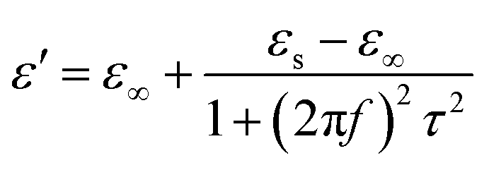
As can be seen from Fig. 7, when the filler content is 10 wt%, the composite with low thickness presents better absorption performance, and shows the maximum RL at the frequency of 10.4 GHz, which can reach the value of −39.0 dB. The effective absorption frequency bandwidth with the RL less than −10 dB is (9.1–12.2 GHz). At the same time, the effective absorption bandwidth is up to 12.2 GHz with the thickness of 2.0–5.0 mm, which exceeds half of the measured frequency range. In view of above mention, the ideal material has a great potential in absorbing with strong absorption, thinness, and wide absorption frequency.
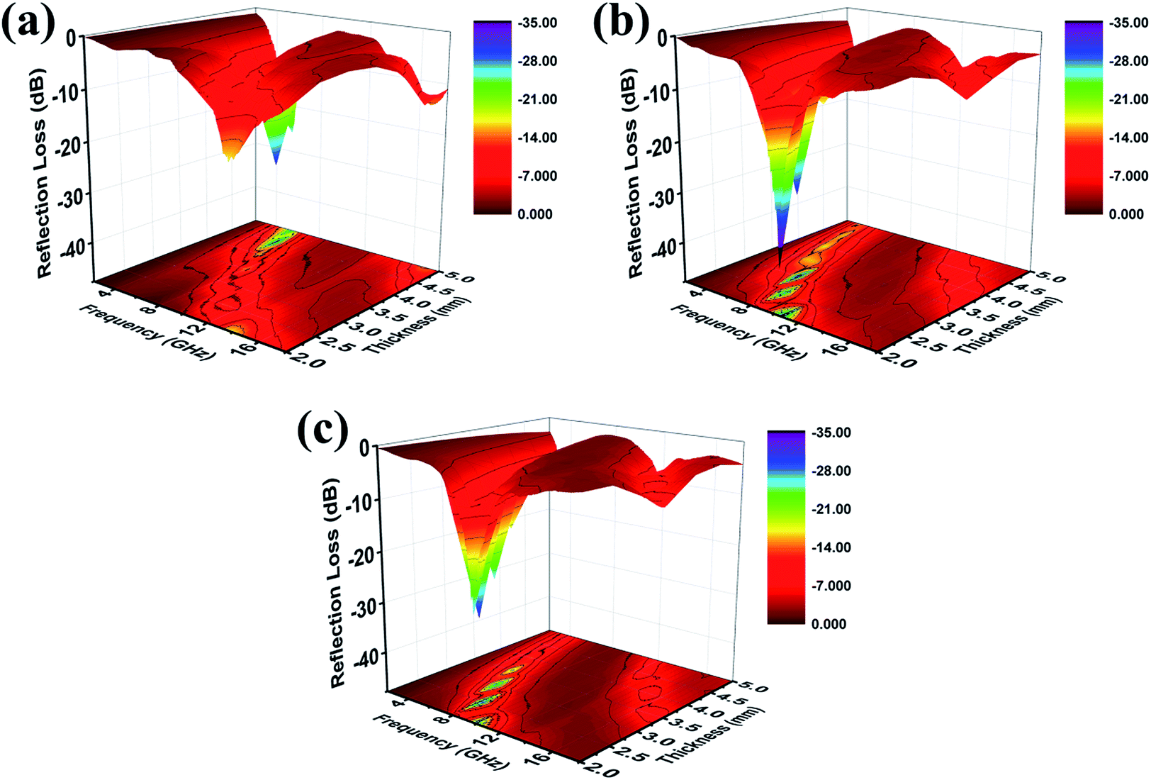 | ||
| Fig. 7 Three-dimensional presentations of the RL of (a) 5 wt%, (b) 10 wt%, (c) 15 wt% Mo2C@C/PVDF in the thickness of 2.0–5.0 mm. | ||
In the analysis of absorption mechanism, Debye dipolar relaxation can make a explanation to the dielectric loss of the composites. According to the Debye theory, ε′ and ε′′ can be described as:34,35
 | (3) |
 | (4) |
According to eqn (3) and (4), the relationship between ε′ and ε′′ can be deduced as:
 | (5) |
The plot of ε′ versus ε′′ thereby forming a single semicircle, normally defined as the Cole–Cole semicircle. Each semicircle means an effective Debye dipolar relaxation process, which is beneficial to microwave absorption.36,37
Debye dipolar relaxations can be derived from electron polarization, ion polarization, orientation polarization and interfacial polarization, etc. The 1D Mo2C@C can be clearly seen the existence of two-phase interface from the TEM image, and the interfacial polarization exists between Mo2C crystals and the outer carbon shell. Fig. S3† displays the ε′–ε′′ curve of 10 wt% Mo2C@C/PVDF, which reveals two semicircles, suggesting that the dielectric loss has been affected by the Debye relaxation, proved the existence of polarization.
Conclusions
In summary, using 1D structural MoO3 nanowires as a precursor, with large aspect ratio and directional transmission ability, the Mo2C@C composite was successfully obtained by carbonation reaction. The final product not only made use of the excellent conductivity of graphitized carbon, but also produced two-phase interface. Therefore, the Mo2C@C/PVDF exhibited excellence microwave absorption performance with 10 wt% filler content, attributing to internal Debye dipolar relaxation. The maximum RL value can reach −39.0 dB, while the absorbing bandwidth was up to 3.1 GHz in the thickness of 2.0 mm. And the effective absorption bandwidth pleasantly covered 12.2 GHz in the thickness of 2.0–5.0 mm. It was believed that the composite can play a promising role in microwave absorption application.Conflicts of interest
There are no conflicts to declare.Acknowledgements
This work was supported by the National Natural Science Foundation of China (No. 51472012), the Fundamental Research Funds for the Central Universities.Notes and references
- J. Liu, R. Che, H. Chen, F. Zhang, F. Xia, Q. Wu and M. Wang, Small, 2012, 8, 1214–1221 CrossRef CAS
.
- Y. Ren, C. Zhu, S. Zhang, C. Li, Y. Chen, P. Gao, P. Yang and Q. Ouyang, Nanoscale, 2013, 5, 12296–12303 RSC
- T. Xia, C. Zhang, N. A. Oyler and X. Chen, Adv. Mater., 2013, 25, 6905–6910 CrossRef CAS
- W. Zhu, L. Wang, R. Zhao, J. Ren, G. Lu and Y. Wang, Nanoscale, 2011, 3, 2862–2864 RSC
- J. Jiang, D. Li, D. Geng, J. An, J. He, W. Liu and Z. Zhang, Nanoscale, 2014, 6, 3967–3971 RSC
- C. Tian, Y. Du, P. Xu, R. Qiang, Y. Wang, D. Ding, J. Xue, J. Ma, H. Zhao and X. Han, ACS Appl. Mater. Interfaces, 2015, 7, 20090–20099 CrossRef CAS
- Y.-F. Pan, G.-S. Wang, L. Liu, L. Guo and S.-H. Yu, Nano Res., 2017, 10, 284–294 CrossRef CAS
- G. Sun, B. Dong, M. Cao, B. Wei and C. Hu, Chem. Mater., 2011, 23, 1587–1593 CrossRef CAS
- S. He, G.-S. Wang, C. Lu, J. Liu, B. Wen, H. Liu, L. Guo and M.-S. Cao, J. Mater. Chem. A, 2013, 1, 4685–4692 RSC
- G.-S. Wang, S. He, X. Luo, B. Wen, M.-M. Lu, L. Guo and M.-S. Cao, RSC Adv., 2013, 3, 18009–18015 RSC
- X. Liu, Y. Chen, X. Cui, M. Zeng, R. Yu and G.-S. Wang, J. Mater. Chem. A, 2015, 3, 12197–12204 RSC
- G. Wang, Z. Gao, S. Tang, C. Chen, F. Duan, S. Zhao, S. Lin, Y. Feng, L. Zhou and Y. Qin, ACS Nano, 2012, 6, 11009–11017 CrossRef CAS
- M. Lu, Q. Wu, X.-H. Guan, W. Xu, H.-Y. Zhang, X. Di, G.-S. Wang and S.-H. Dong, Front. Chem., 2018, 6, 405 CrossRef CAS
- H.-L. Zhu, Y.-J. Bai, R. Liu, N. Lun, Y.-X. Qi, F.-D. Han and J.-Q. Bi, J. Mater. Chem., 2011, 21, 13581–13587 RSC
- M.-S. Cao, W.-L. Song, Z.-L. Hou, B. Wen and J. Yuan, Carbon, 2010, 48, 788–796 CrossRef CAS
- W. Xu, Y.-F. Pan, W. Wei, G.-S. Wang and P. Qu, Appl. Surf. Sci., 2018, 428, 54–60 CrossRef CAS
- Z. Xu, Y. Du, D. Liu, Y. Wang, W. Ma, Y. Wang, P. Xu and X. Han, ACS Appl. Mater. Interfaces, 2019, 11, 4268–4277 CrossRef CAS
- D. Ding, Y. Wang, X. Li, R. Qiang, P. Xu, W. Chu, X. Han and Y. Du, Carbon, 2017, 111, 722–732 CrossRef CAS
- T. Wu, Y. Liu, X. Zeng, T. Cui, Y. Zhao, Y. Li and G. Tong, ACS Appl. Mater. Interfaces, 2016, 8, 7370–7380 CrossRef CAS
- H. Lin, Z. Shi, S. He, X. Yu, S. Wang, Q. Gao and Y. Tang, Chem. Sci., 2016, 7, 3399–3405 RSC
- S. Dai, Y. Cheng, B. Quan, X. Liang, W. Liu, Z. Yang, G. Ji and Y. Du, Nanoscale, 2018, 10, 6945–6953 RSC
- Y. Wang, X. Han, P. Xu, D. Liu, L. Cui, H. Zhao and Y. Du, Chem. Eng. J., 2019, 372, 312–320 CrossRef CAS
- I. Shakir, M. Shahid, U. A. Rana and M. F. Warsi, RSC Adv., 2014, 4, 8741–8745 RSC
- Y. Luo, Z. Wang, Y. Fu, C. Jin, Q. Wei and R. Yang, J. Mater. Chem. A, 2016, 4, 12583–12590 RSC
- Y. Wang, C. Li, X. Han, D. Liu, H. Zhao, Z. Li, P. Xu and Y. Du, ACS Appl. Nano Mater., 2018, 1, 5366–5376 CrossRef CAS
- Y.-F. Pan, G.-S. Wang and Y.-H. Yue, RSC Adv., 2015, 5, 71718–71723 RSC
- X.-J. Zhang, G.-S. Wang, W.-Q. Cao, Y.-Z. Wei, J.-F. Liang, L. Guo and M.-S. Cao, ACS Appl. Mater. Interfaces, 2014, 6, 7471–7478 CrossRef CAS
- X. Jian, B. Wu, Y. Wei, S. X. Dou, X. Wang, W. He and N. Mahmood, ACS Appl. Mater. Interfaces, 2016, 8, 6101–6109 CrossRef CAS
- W. Xu, G.-S. Wang and P.-G. Yin, Carbon, 2018, 139, 759–767 CrossRef CAS
- Y. Yang, L. Xia, T. Zhang, B. Shi, L. Huang, B. Zhong, X. Zhang, H. Wang, J. Zhang and G. Wen, Chem. Eng. J., 2018, 352, 510–518 CrossRef CAS
- J. Deng, Q. Wang, Y. Zhou, B. Zhao and R. Zhang, RSC Adv., 2017, 7, 9294–9302 RSC
- J. Liu, J. Cheng, R. Che, J. Xu, M. Liu and Z. Liu, J. Phys. Chem. C, 2013, 117, 489–495 CrossRef CAS
- A. Yan, Y. Liu, Y. Liu, X. Li, Z. Lei and P. Liu, Mater. Lett., 2012, 68, 402–405 CrossRef CAS
- X.-M. Meng, X.-J. Zhang, C. Lu, Y.-F. Pan and G.-S. Wang, J. Mater. Chem. A, 2014, 2, 18725–18730 RSC
- G.-S. Wang, X.-J. Zhang, Y.-Z. Wei, S. He, L. Guo and M.-S. Cao, J. Mater. Chem. A, 2013, 1, 7031–7036 RSC
- H. Yu, T. Wang, B. Wen, M. Lu, Z. Xu, C. Zhu, Y. Chen, X. Xue, C. Sun and M. Cao, J. Mater. Chem., 2012, 22, 21679–21685 RSC
- X.-J. Zhang, J.-Q. Zhu, P.-G. Yin, A.-P. Guo, A.-P. Huang, L. Guo and G.-S. Wang, Adv. Funct. Mater., 2018, 28, 1800761 CrossRef
Footnote |
| † Electronic supplementary information (ESI) available. See DOI: 10.1039/c9ra03362a |
| This journal is © The Royal Society of Chemistry 2019 |