
 Open Access Article
 This Open Access Article is licensed under a Creative Commons Attribution-Non Commercial 3.0 Unported Licence
High-energy proton irradiation damage on two-dimensional hexagonal boron nitride†
Dongryul Lee‡
a,
Sanghyuk Yoo‡ b,
Jinho Baea,
Hyunik Parka,
Keonwook Kang*b and
Jihyun Kim*a
b,
Jinho Baea,
Hyunik Parka,
Keonwook Kang*b and
Jihyun Kim*a
aDepartment of Chemical and Biological Engineering, Korea University, Seoul 02841, South Korea. E-mail: hyunhyun7@korea.ac.kr
bDepartment of Mechanical Engineering, Yonsei University, Seoul 03722, South Korea. E-mail: kwkang75@yonsei.ac.kr
First published on 11th June 2019
Abstract
The dielectric layer, which is an essential building block in electronic device circuitry, is subject to intrinsic or induced defects that limit its performance. Nano-layers of hexagonal boron nitride (h-BN) represent a promising dielectric layer in nano-electronics owing to its excellent electronic and thermal properties. In order to further analyze this technology, two-dimensional (2D) h-BN dielectric layers were exposed to high-energy proton irradiation at various proton energies and doses to intentionally introduce defective sites. A pristine h-BN capacitor showed typical degradation stages with a hard breakdown field of 10.3 MV cm−1, while h-BN capacitors irradiated at proton energies of 5 and 10 MeV at a dose of 1 × 1013 cm−2 showed lower hard breakdown fields of 1.6 and 8.3 MV cm−1, respectively. Higher leakage currents were observed under higher proton doses at 5 × 1013 cm−2, resulting in lower breakdown fields. The degradation stages of proton-irradiated h-BN are similar to those of defective silicon dioxide. The degradation of the h-BN dielectric after proton irradiation is attributed to Frenkel defects created by the high-energy protons, as indicated by the molecular dynamics simulation. Understanding the defect-induced degradation mechanism of h-BN nano-layers can improve their reliability, paving the way to the implementation of 2D h-BN in advanced micro- and nano-electronics.
Introduction
Hexagonal boron nitride (h-BN) with sp2-hybridized bonds is a unique material with excellent chemical and thermal stabilities, superior lubricity, high thermal conductivity (∼400 W m−1 K−1 in-plane),1 and an ultra-wide bandgap energy (5.2–5.9 eV at room temperature),2 which make it an electrical insulator, a thermal conductor, a lubricator, and an anti-oxidant.3 Therefore, it has versatile applications, such as in electronic devices, anti-corrosion coatings, lubricants, cosmetics, and paints.4,5 H-BN has a layered structure characterized by weak out-of-plane interactions between layers due to van der Waals forces and strong in-plane covalent bonds between sp2-hybridized B and N atoms within layers. Successful growth of two-dimensional (2D) h-BN by chemical vapor deposition has been reported, demonstrating its scalability and compatibility with microelectronic fabrication processes.6 In addition, a 2D form of h-BN can be obtained from the bulk crystal by mechanical, liquid, or chemical exfoliation methods, and retains the excellent electrical, thermal, and chemical properties of the bulk material. Laturia et al. investigated the dielectric properties of bulk and monolayer h-BN,7 while Hui et al. reviewed the use of h-BN as a 2D dielectric.6 Jo et al. reported that suspended few-layer h-BN exhibited excellent thermal properties comparable to those observed for the basal plane of bulk h-BN.1Dielectrics are essential layers in advanced microelectronics and near-future nano-electronics. Currently, the continuous down-scaling of device dimensions necessitates the replacement of SiO2 with novel dielectrics, as the leakage current in ultra-thin SiO2 layers becomes unacceptably high.8 Isolation of the conductors in advanced multi-level interconnect systems also requires a more suitable dielectric layer. Although novel dielectrics such as Al2O3 and HfOx help to mitigate the leakage current,9 they create additional problems related to interface states, interfacial charges, and unwanted interactions with the semiconductor and metal electrodes. Owing to the absence of dangling bonds on the surface, 2D dielectrics like h-BN are supposed to have no interface state or surface charge, and are compatible with other van der Waals materials, including transition metal dichalcogenides (TMDs), graphene, and black phosphorus.6,10 The ultra-thinness of 2D h-BN and its high breakdown field (intrinsically 8–12 MV cm−1) allow facile electrostatic control of the channel layer in field-effect transistors (FETs).11,12 In addition, its atomic flatness with no surface charge is attractive for high-performance FETs owing to its fewer carrier scattering centers.5 Various nano-devices integrated with 2D h-BN have been reported, e.g., metal–insulator–semiconductor FETs (MISFETs) with 2D h-BN as a gate dielectric and a channel layer comprising 2D TMDs.13 Lee et al. investigated tunneling transport in an ultra-thin h-BN layer and reported a high dielectric strength of 7.94 MV cm−1 for the 2D form.14
The performance of the dielectric layer is limited by the types of defects and their density, which, in turn, determine device reliability. The defects that can act as a leakage path threaten the lifetime of electronic devices, including capacitors and MISFETs.15 In addition, charged defect centers in the dielectric may re-distribute the electric field in the active channel layer, shifting the threshold voltage of FETs. Once created, the defect centers can move, grow, and be annihilated, affecting device performance and stability.16,17 Therefore, the investigation of defect centers in 2D h-BN is of fundamental and practical importance. Furthermore, nano-electronics with excellent specific power handling capacity have great potential for space applications, allowing for the miniaturization of electronic parts. Generally, the large volume of material surrounding an electronic device would absorb the incoming high-energy particles before they could damage the electronic devices. The polyethylene which is common plastic products has been used for radiation shielding due to its high hydrogen concentration and low cost. The radiation hardness of 2D h-BN-based capacitors is important to ensure the long-term reliability of h-BN-based electronic devices for space missions. In our experiments, various defect centers were intentionally created within 2D h-BN via high-energy proton irradiation at different energies and doses, which duplicates the environments encountered beyond the Earth's atmosphere. The degradation of 2D h-BN under high-energy proton irradiation was simulated by numerical analysis, and the results agreed with those obtained experimentally for a proton-irradiated h-BN nano-capacitor.
Experimental details
Fig. 1(a–d) provide schematics of the fabrication procedure. The source and drain electrodes (Ti/Au 20 nm/80 nm) were defined on a SiO2/p++-Si (300 nm/525 μm) substrate using a standard photolithography process and electron-beam evaporation (Fig. 1(a)), and the distance between electrodes was set to 16 μm. H-BN flakes, with thicknesses of 30–50 nm, were mechanically cleaved from high-purity h-BN bulk crystal (Momentive Performance Materials) using a commercial adhesive tape. The exfoliated h-BN flakes were dry-transferred onto a pre-patterned substrate, as shown in Fig. 1(b), and subjected to 5 or 10 MeV proton irradiation at doses of 1 × 10¹³ and 5 × 1013 cm−2. The high-energy proton beam generated using the MC-50 Cyclotron at the Korea Institute of Radiological and Medical Science was introduced into a low-vacuum chamber in which the h-BN based devices were loaded facing the proton beam. The average beam current, measured by a Faraday cup, was 100 nA during the proton irradiation process. The durations of proton irradiation were 11 and 55 s, which corresponded to fluences of 1 × 10¹³ and 5 × 1013 cm−2, respectively. The proton beam was uniformly irradiated over an area of 1 cm × 1 cm, and beam uniformity was monitored using a radiation-sensitive film (Gafchromic MD-V2). Electrical and optical characterizations were performed a few days after the proton irradiation because of safety regulations. After proton irradiation (Fig. 1(c)), multi-layer graphene (GPN, HQ graphene) flakes exfoliated from highly oriented pyrolytic graphite were dry-transferred onto the proton irradiated h-BN and one of the Ti/Au electrodes to complete the vertical capacitor structure, as shown in Fig. 1(d). The heterostructure of graphene/h-BN has been widely used in 2D electronics, as the small lattice mismatch (1.7%) between graphene and h-BN allows good adhesion.18 Multi-layer graphene served as the top electrode, and the Ti/Au electrode under the h-BN layer acted as the bottom electrode.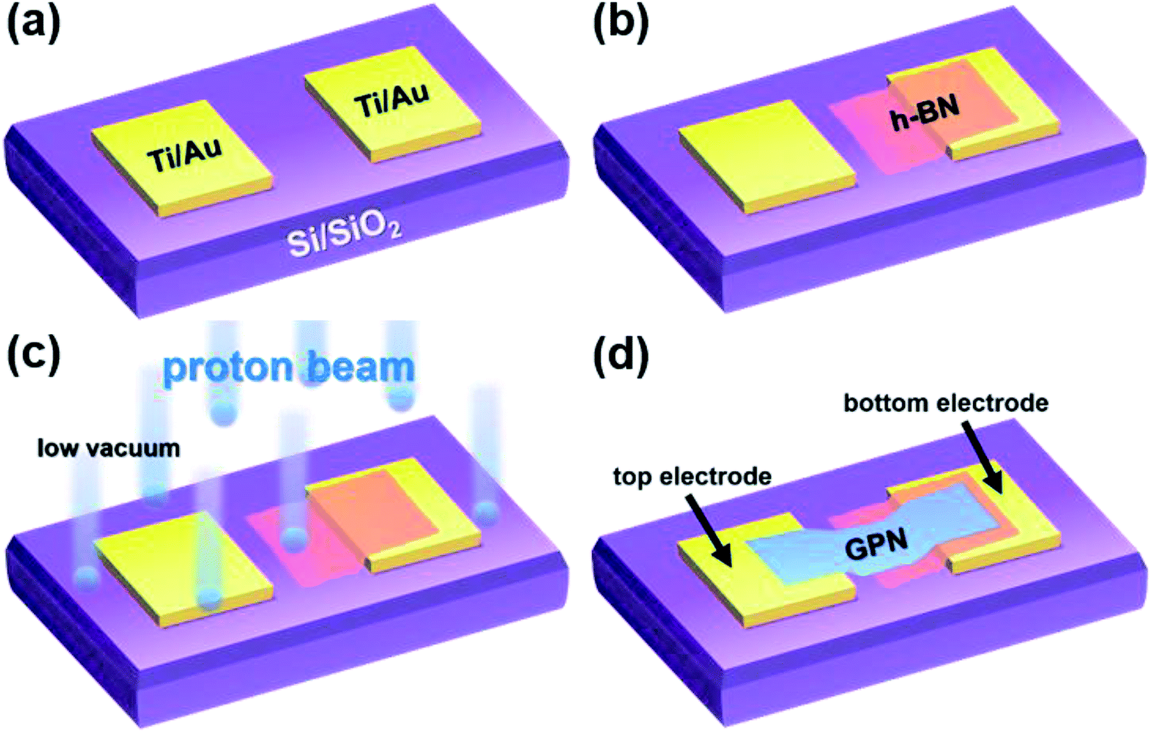 | ||
| Fig. 1 Schematics of h-BN nano-capacitor fabrication process and proton irradiation. (a) Ti/Au contacts (bottom electrode) were defined on SiO2/Si substrate. (b) Exfoliated h-BN (dielectric) was dry-transferred onto the pre-patterned substrate. (c) The sample was irradiated with high-energy protons. (d) Exfoliated graphene was dry-transferred onto the irradiated sample to complete the vertical capacitor structure. | ||
The thickness of the h-BN layer was measured by atomic force microscopy (AFM; Bruker, Innova) in tapping mode. The optical properties of the fabricated capacitor were analyzed by micro-Raman spectroscopy using a 532 nm-wavelength diode-pumped solid-state laser (Omicron) in a back-scattering geometry, and morphology was evaluated by high-resolution scanning electron microscopy (SEM; HITACHI, SU-70). The electrical characterization of the capacitor was performed using a semiconductor parameter analyzer (Agilent, 4155C) and an LCR meter (Agilent, 4285A) connected to a low-vacuum (∼6 mTorr) probe station.
The primary knock-on atom (PKA) approach was used to mimic energy and momentum transfer from proton collisions in molecular dynamics (MD) simulations of h-BN irradiation. In these simulations, a B atom is projected with a prescribed amount of kinetic energy, as if it collided with an incoming proton. The simulation system consists of 32 h-BN layers, and the number of atoms is 61![[thin space (1/6-em)]](https://www.rsc.org/images/entities/char_2009.gif) 440 for both B and N. The Tersoff potential model is used to simulate B–B, N–N, and B–N interactions.19 The simulation cell size is approximately 10.1 × 10.5 × 10.5 nm3, and the periodic boundary condition is applied in all directions. PKA simulations were conducted after the structure reached a thermodynamic equilibrium state at 300 K and 0 Pa. Atoms in the outermost layers of two-lattice thickness were fixed to maintain the AA′′-stacking sequence during the simulation. The atoms in a volume of four-lattice thicknesses inside the fixed volume were thermostated by applying the Nosé–Hoover algorithm to maintain the temperature of the entire system at 300 K. A microcanonical (NVE) MD simulation was applied to the rest of the cell. A B atom, initially located ∼8.5 nm from the bottom of the simulation cell, was launched along the z direction with a PKA energy of 1 keV, which, according to Stephani and Boyd, is high enough to produce defect formation in h-BN.20 The time step was chosen to be as short as 0.01 fs to prevent tracking loss of atoms with high energy during PKA simulations. The total simulation time equaled 2.0 ps.
440 for both B and N. The Tersoff potential model is used to simulate B–B, N–N, and B–N interactions.19 The simulation cell size is approximately 10.1 × 10.5 × 10.5 nm3, and the periodic boundary condition is applied in all directions. PKA simulations were conducted after the structure reached a thermodynamic equilibrium state at 300 K and 0 Pa. Atoms in the outermost layers of two-lattice thickness were fixed to maintain the AA′′-stacking sequence during the simulation. The atoms in a volume of four-lattice thicknesses inside the fixed volume were thermostated by applying the Nosé–Hoover algorithm to maintain the temperature of the entire system at 300 K. A microcanonical (NVE) MD simulation was applied to the rest of the cell. A B atom, initially located ∼8.5 nm from the bottom of the simulation cell, was launched along the z direction with a PKA energy of 1 keV, which, according to Stephani and Boyd, is high enough to produce defect formation in h-BN.20 The time step was chosen to be as short as 0.01 fs to prevent tracking loss of atoms with high energy during PKA simulations. The total simulation time equaled 2.0 ps.
Results and discussion
Fig. 2(a) presents an AFM image of the fabricated h-BN capacitor, revealing a vertical structure with exfoliated graphene as the top electrode and Ti/Au contacts as the bottom electrode. Graphene was connected to the neighboring Ti/Au bond pad as shown in Fig. 1(d). Nano-layer h-BN exfoliated with a uniform thickness (30–50 nm) was transferred on top of the bottom electrode. The top and bottom electrodes were electrically isolated by the exfoliated h-BN flake, which has a clear interface without any tears, indicating good physical stability and durability. Micro-Raman spectroscopy was performed to analyze the quality of the h-BN and graphene. Fig. 2(b) shows the Raman spectrum of the graphene used as the top electrode in the fabricated capacitor, where it exhibits a (very weak) D peak at ∼1350 cm−1, a G peak at ∼1580 cm−1, and a 2D peak at ∼2700 cm−1. The quality of graphene can be analyzed using the intensity ratio of the D and G peaks (ID/IG).21 For pristine graphene, the ID/IG ratio equals 0.05 and thus indicated a low defect level and high crystallinity. The Raman spectrum of the h-BN flake used as the dielectric material is shown in Fig. 2(c). The phonon peak (E2g) of h-BN was observed at ∼1370 cm−1, with the full width at half maximum of this peak determined as 22.1 cm−1.8 The capacitance of the fabricated h-BN nano-capacitor was measured to be 0.36 pF by using the LCR meter, which is in good agreement with the calculated capacitance (0.33 pF) from the following equation: , where C is the capacitance, ε is the dielectric constant, and A is the contact area. Ahmed et al. reported the dispersion characteristics of multi-layer h-BNs at different thickness and temperatures, demonstrating its potential as a dielectric material.22 The thickness (d) of h-BN was determined to be 41 nm by AFM analysis. SEM imaging of the as-fabricated (pristine) sample confirmed that the top electrode was electrically isolated from the bottom electrode by the h-BN nanolayer (Fig. 3(a)). Fig. 3(b) shows the dielectric breakdown characteristics of the pristine h-BN samples. The hard breakdown fields of four pristine h-BN capacitors were averaged to 10.3 MV cm−1, which agreed with previously reported values of 8–12 MV cm−1.11,12,23 To investigate the dielectric properties of h-BN under an electric field, the Fowler–Nordheim (F–N) plot (Fig. 3(c)) was obtained from the following relationship:
where JF–N is the current density, EOX is the electric field, ln(A) is the y-intercept, and −B is the slope.24 Direct tunneling was observed at low electric fields. As the electric field increases, F–N tunneling through the triangular energy barrier occurs, indicating that the h-BN used in this study possesses excellent dielectric properties.14
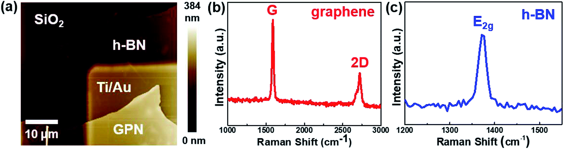 | ||
| Fig. 2 (a) AFM image of the as-fabricated (pristine) h-BN nano-capacitor. Raman spectra of the (b) graphene and (c) h-BN before proton irradiation. | ||
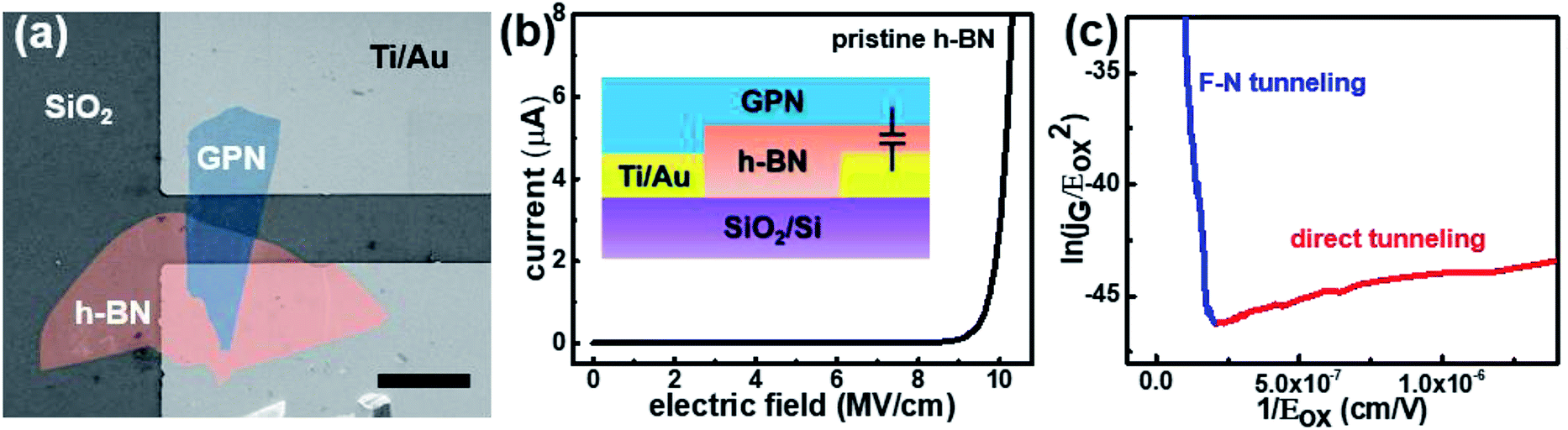 | ||
| Fig. 3 (a) SEM image of the as-fabricated h-BN nano-capacitor (b) current–electric field data of the pristine h-BN nano-capacitor (inset: structure of the h-BN nano-capacitor) (c) F–N plot of the pristine h-BN nano-capacitor. | ||
The dielectric breakdown fields obtained for pristine and proton-irradiated h-BN are compared in Fig. 4 and Table 1. A lower hard breakdown field was observed for proton-irradiated samples than for the pristine sample. Note that the top electrode (graphene) was deposited after proton irradiation and therefore did not experience this irradiation. Table 1 shows that F–N tunneling occurred at a lower electric field when h-BN was proton-irradiated, which was indicative of hopping conduction among the induced defects. The effects of proton irradiation on F–N tunneling were in good agreement with those of proton irradiation on the hard breakdown field. At the same proton energy, the higher the doses were, the lower the breakdown fields were. The h-BN irradiated at doses of 1 × 10¹³ and 5 × 1013 cm−2 at an energy of 5 MeV exhibited hard breakdown fields of 1.6 and 1.1 MV cm−1, respectively, owing to the increased probability of damaging events. At the same proton dose of 1 × 10¹³, the breakdown field of the h-BN proton-irradiated at 5 MeV is lower than that of the sample irradiated at 10 MeV by 6.7 MV cm−1 because the lower energy protons that experience the larger Coulomb interaction have higher probability of colliding with the nucleus.15
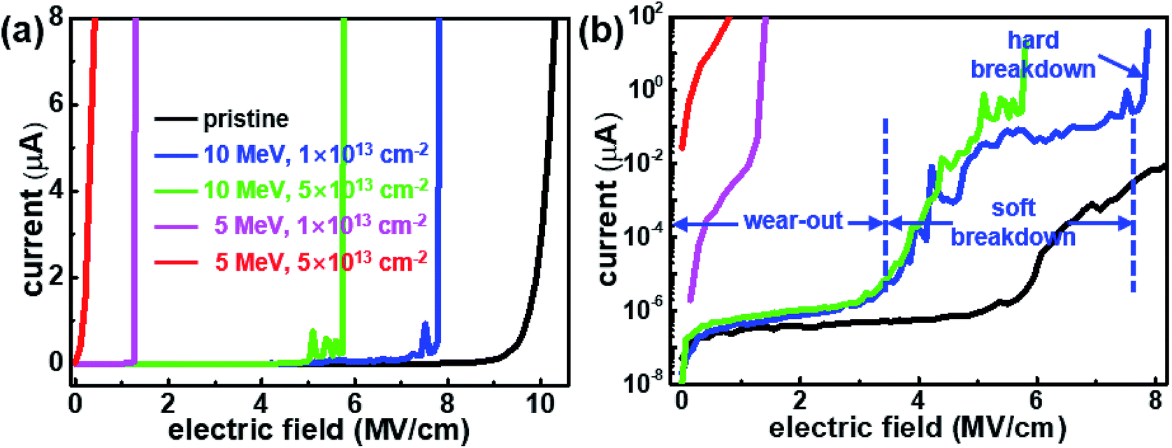 | ||
| Fig. 4 Current–electric field characteristics of the pristine and proton-irradiated h-BN nano-capacitors at different energies and doses in (a) a linear scale, and (b) a log scale. | ||
| Electric field (MV cm−1) | Proton irradiation | ||||
|---|---|---|---|---|---|
| Pristine | 10 MeV, 1 × 1013 cm−2 | 10 MeV, 5 × 1013 cm−2 | 5 MeV, 1 × 1013 cm−2 | 5 MeV, 5 × 1013 cm−2 | |
| F–N tunneling onset | 4.8 | 2.7 | 2.6 | 1.1 | 0.5 |
| Hard breakdown | 10.3 | 8.3 | 6.6 | 1.6 | 1.1 |
The breakdown stages of 2D h-BN dielectric layer were analyzed at varying applied electric field, as shown in Fig. 4(b). When an electric field is applied in the h-BN capacitor, the leakage currents gradually increase, which is similar to the behavior of the stress-induced leakage current (wear-out) in SiO2. This wear-out stage is reported to occur at 3–5 MV cm−1 in high-quality SiO2.25 When the electric field continuously increases, it causes electrons to move away from the trap. Through this process, the holes accumulated in the trap are accelerated under the high electric field, resulting in a defect-related conduction path.25 Aggregation of such paths generates a filament in which the leakage current can flow at a local scale. Soft (or quasi) breakdown is commonly defined as an instantaneous increase in leakage current due to the existence of multiple filaments.26 When the applied electric field is further increased after soft breakdown, an irreversible current path appears, resulting in large current flow. In this study, hard (catastrophic) breakdown is defined as the stage in which the dielectric material permanently loses its insulating capacity.26 After the introduction of defects, the wear-out period becomes shorter, reaching the soft/hard breakdown at lower electric fields than for pristine h-BN as shown in Fig. 4(b). In SiO2, the three breakdown modes (A, B, and C) are well understood according to the type and density of the defects or surface states.25 The breakdown of high-quality SiO2 occurs in the C-mode, which is similar to that of pristine h-BN. The B-mode SiO2 dielectric breakdown caused by the presence of oxide thinning and by other defects was in good agreement with that of the h-BN proton-irradiated at 10 MeV, as shown in Fig. 4(b). The most severely damaged h-BN having a breakdown field of less than 2 MV cm−1 exhibited breakdown behavior similar to that of A-mode SiO2, which contains pinhole and gross defects.
MD simulations of h-BN were employed to identify the defects created by high-energy proton irradiation and to relate them with the electrical measurements. PKA simulations were conducted to investigate what types of defects are generated under high-energy proton irradiation. Fig. 5 shows the process of defect formation during a PKA simulation from 0 to 0.35 fs at 0.05 fs intervals. The locations of the defects depicted in this figure are subsequent collision points located 4.5 nm above the bottom of the simulation cell. Initially (0–0.10 fs), the atoms appear to form a locally amorphous structure, but most of them are subsequently restored to lattice positions and form the original h-BN structure. Additional defect generation is not observed after 0.35 fs. The remaining defects in h-BN identified through the PKA simulation are classified as Frenkel defects and include interstitials, vacancies, and anti-sites. According to density functional theory (DFT) calculations, these defects, which can have various charge states, act as trap sites in the electronic band structure.27 As expected from previous experiments, trap-assisted tunneling can occur more readily after proton irradiation. In Fig. 6, a vacancy cluster is observed in the h-BN layer, while the atoms that were previously part of the h-BN layer are located between the h-BN layers and form an interstitial cluster. In particular, the fact that N atoms are paired with N2 molecules also agrees with the results of previous DFT calculations.27 The interstitial cluster connects the h-BN layers and becomes a breakdown path in the semiconductor device, as is known in percolation theory. Our simulation results support the formation of a conduction path during proton irradiation, as suggested by the experimental results. Interstitial clusters generated between proton-irradiated h-BN layers create a conduction filament through which electrons can flow.
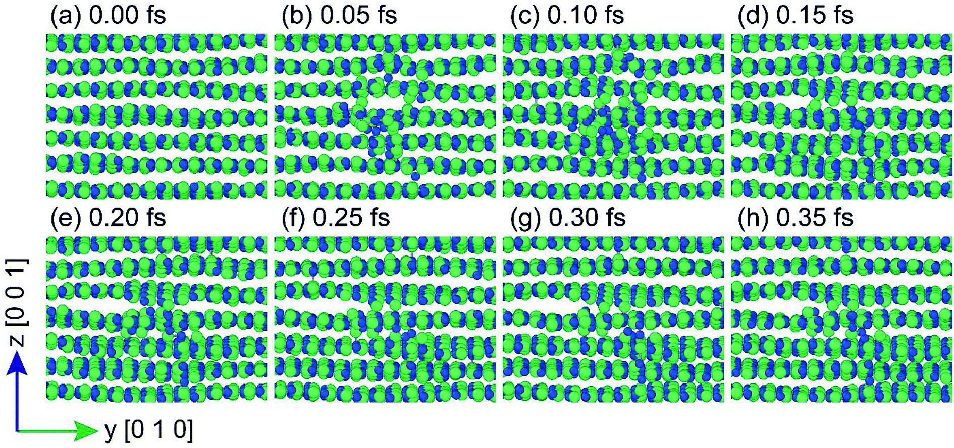 | ||
| Fig. 5 Defect growth between 0 and 0.35 fs. Images were captured from the [100] direction. Solid green and blue circles represent B and N atoms, respectively. | ||
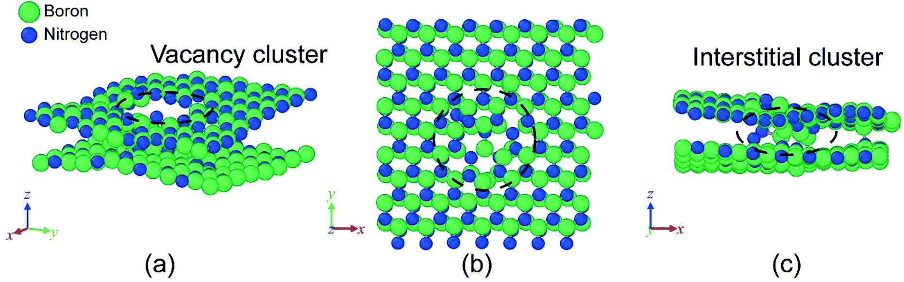 | ||
Fig. 6 Damage predicted by MD simulation (a) orthogonal view at [![[4 with combining macron]](https://www.rsc.org/images/entities/char_0034_0304.gif) ![[2 with combining macron]](https://www.rsc.org/images/entities/char_0032_0304.gif) ![[1 with combining macron]](https://www.rsc.org/images/entities/char_0031_0304.gif) ] and views of (b) xy plane and (c) zx plane. Solid green and blue circles represent boron and nitrogen atoms, respectively. ] and views of (b) xy plane and (c) zx plane. Solid green and blue circles represent boron and nitrogen atoms, respectively. | ||
Conclusion
To systematically investigate the effects of defects on the dielectric breakdown of 2D h-BN, defects were intentionally introduced by exposing 2D h-BN to high-energy proton irradiation (5 or 10 MeV) at different doses. The nano-capacitor fabricated using pristine 2D h-BN exhibited an excellent hard breakdown field of 10.3 MV cm−1, which is comparable to that of high-quality SiO2. Direct and F–N tunneling behaviors were investigated in pristine and defect-induced 2D h-BN under the applied electric fields. The breakdown stages, including wear-out, and soft and hard breakdowns, were analyzed before and after proton irradiation. Defects induced by proton irradiation at an energy of 5 MeV lowered the hard breakdown fields to values of <2 MV cm−1 that were comparable to those previously obtained for defective SiO2. Increased proton radiation fluency resulted in more severe h-BN degradation and hence a lower breakdown field. The evolution of defects under proton irradiation was numerically simulated, and the obtained results suggested the formation of Frenkel defects in h-BN. We believe that a deep understanding of defect formation-induced degradation of h-BN can help to improve the reliability of h-BN-based micro- and nano-electronics in hostile environments.Conflicts of interest
There are no conflicts to declare.Acknowledgements
This research was supported by the Space Core Technology Development Program (2017M1A3A3A02015033) through the National Research Foundation of Korea funded by the Ministry of Science, ICT and Future Planning of Korea.References
- I. Jo, M. T. Pettes, J. Kim, K. Watanabe, T. Taniguchi, Z. Yao and L. Shi, Thermal conductivity and phonon transport in suspended few-layer hexagonal boron nitride, Nano Lett., 2013, 13(2), 550–554 CrossRef CAS.
- K. Watanabe, T. Taniguchi and H. Kanda, Direct-bandgap properties and evidence for ultraviolet lasing of hexagonal boron nitride single crystal, Nat. Mater., 2004, 3(6), 404–409 CrossRef CAS PubMed.
- X. F. Jiang, Q. Weng, X. B. Wang, X. Li, J. Zhang, D. Golberg and Y. Bando, Recent progress on fabrications and applications of boron nitride nanomaterials: a review, J. Mater. Sci. Technol., 2015, 31(6), 589–598 CrossRef.
- J. Bae, H. W. Kim, I. H. Kang, G. Yang and J. Kim, High breakdown voltage quasi-two-dimensional beta-Ga2O3 field-effect transistors with a boron nitride field plate, Appl. Phys. Lett., 2018, 112(12), 122102 CrossRef.
- D. Li, M. Chen, Z. Sun, P. Yu, Z. Liu, P. M. Ajayan and Z. Zhang, Two-dimensional non-volatile programmable p–n junctions, Nat. Nanotechnol., 2017, 12(9), 901–906 CrossRef CAS PubMed.
- F. Hui, C. Pan, Y. Shi, Y. Ji, E. G. Gutierrez and M. Lanza, On the use of two dimensional hexagonal boron nitride as dielectric, Microelectron. Eng., 2016, 163, 119–133 CrossRef CAS.
- A. Laturia, M. L. Van de Put and W. G. Vandenberghe, Dielectric properties of hexagonal boron nitride and transition metal dichalcogenides: from monolayer to bulk, npj 2D Mater. Appl., 2018, 2, 6 CrossRef.
- L. H. Li, E. J. G. Santos, T. Xing, E. Cappelluti, R. Roldán, Y. Chen, K. Watanabe and T. Taniguchi, Dielectric screening in atomically thin boron nitride nanosheets, Nano Lett., 2015, 15(1), 218–223 CrossRef CAS PubMed.
- R. Suzuki, N. Taoka, M. Yokoyama, S. Lee, S. H. Kim, T. Hoshi, T. Yasuda, W. Jevasuwan, T. Maeda, O. Ichikawa, N. Fukuhara, M. Hata, M. Takenaka and S. Takagi, 1-nm-capacitance-equivalent-thickness HfO2/Al2O3/InGaAs metal-oxide-semiconductor structure with low interface trap density and low gate leakage current density, Appl. Phys. Lett., 2012, 100(13), 132906 CrossRef.
- L. H. Li, J. Cervenka, K. Watanabe, T. Taniguchi and Y. Chen, Strong oxidation resistance of atomically thin boron nitride nanosheets, ACS Nano, 2014, 8(2), 1457–1462 CrossRef CAS PubMed.
- Y. Hattori, T. Taniguchi, K. Watanabe and K. Nagashio, Layer-by-layer dielectric breakdown of hexagonal boron nitride, ACS Nano, 2015, 9(1), 916–921 CrossRef CAS PubMed.
- Y. Ji, C. Pan, M. Zhang, S. Long, X. Lian, F. Miao, F. Hui, Y. Shi, L. Larcher, E. Wu and M. Lanza, Boron nitride as two dimensional dielectric: reliability and dielectric breakdown, Appl. Phys. Lett., 2016, 108(1), 012905 CrossRef.
- J. Kim, M. A. Mastro, M. J. Tadjer and J. Kim, Quasi-two-dimensional h-BN/beta-Ga2O3 heterostructure metal-insulator-semiconductor field-effect transistor, ACS Appl. Mater. Interfaces, 2017, 9(25), 21322–21327 CrossRef CAS PubMed.
- G. H. Lee, Y. J. Yu, C. Lee, C. Dean, K. L. Shepard, P. Kim and J. Hone, Electron tunneling through atomically flat and ultrathin hexagonal boron nitride, Appl. Phys. Lett., 2011, 99(24), 243114 CrossRef.
- H. Y. Kim, J. Kim, L. Liu, C. F. Lo, F. Ren and S. J. Pearton, Effects of proton irradiation energies on degradation of AlGaN/GaN high electron mobility transistors, J. Vac. Sci. Technol., 2012, 30(1), 012202 CrossRef.
- S. Lee, J. Seo, J. Hong, S. H. Park, J. H. Lee, B. W. Min and T. Lee, Proton irradiation energy dependence of defect formation in graphene, Appl. Surf. Sci., 2015, 344, 52–56 CrossRef CAS.
- H. N. M. Duong, M. A. P. Nguyen, M. Kianinia, T. Ohshima, H. Abe, K. Watanabe, T. Taniguchi, J. H. Edgar, I. Aharonovich and M. Toth, Effects of high-energy electron irradiation on quantum emitters in hexagonal boron nitride, ACS Appl. Mater. Interfaces, 2018, 10(29), 24886–24891 CrossRef PubMed.
- C. R. Dean, A. F. Young, I. Meric, C. Lee, L. Wang, S. Sorgenfrei, K. Watanabe, T. Taniguchi, P. Kim, K. L. Shepard and J. Hone, Boron nitride substrates for high-quality graphene electronics, Nat. Nanotechnol., 2010, 5(10), 722–726 CrossRef CAS PubMed.
- K. Albe, W. Möller and K. H. Heinig, Computer simulation and boron nitride, Radiat. Eff. Defects Solids, 1997, 141(1–4), 85–97 CrossRef CAS.
- K. A. Stephani and I. D. Boyd, Molecular dynamics modeling of defect formation in many-layer hexagonal boron nitride, Nucl. Instrum. Methods Phys. Res., Sect. B, 2015, 365, 235–239 CrossRef CAS.
- L. G. Cancado, A. Jorio, E. H. M. Ferreira, F. Stavale, C. A. Achete, R. B. Capaz, M. V. O. Moutinho, A. Lombardo, T. S. Kulmala and A. C. Ferrari, Quantifying defects in graphene via Raman spectroscopy at different excitation energies, Nano Lett., 2011, 11(8), 3190–3196 CrossRef CAS PubMed.
- F. Amned, S. Heo, Z. Yang, F. Ali, C. H. Ra, H.-I. Lee, T. Taniguchi, J. Hone, B. H. Lee and W. J. Yoo, Dielectric Dispersion and High Field Response of Multilayer Hexagonal Boron Nitride, Adv. Funct. Mater., 2018, 1804235 Search PubMed.
- Y. Hattori, T. Taniguchi, K. Watanabe and K. Nagashio, Anisotropic dielectric breakdown strength of single crystal hexagonal boron nitride, ACS Appl. Mater. Interfaces, 2016, 8(41), 27877–27884 CrossRef CAS PubMed.
- D. K. Schroder, Semiconductor Material and Device Characterization, John Wiley and Sons, Inc., New York, 2nd edn, 1998, pp. 391–394 Search PubMed.
- J. T. You, Reliability, in ULSI Technology, C. Y. Chang and S. M. Sze, The McGraw-Hill Companies, Inc., New York, 1996, pp. 679–682 Search PubMed.
- C. Claeys and E. Simoen, Radiation Effects in Advanced Semiconductor Materials and Devices, Springer, Berlin, 2002, pp. 216–226 Search PubMed.
- L. Weston, D. Wickramaratne, M. Mackoit, A. Alkauskas and C. G. Van de Walle, Native point defects and impurities in hexagonal boron nitride, Phys. Rev. B, 2018, 97(21), 214104 CrossRef CAS.
Footnotes |
| † Electronic supplementary information (ESI) available. See DOI: 10.1039/c9ra03121a |
| ‡ D. Lee and S. Yoo contributed equally to this work. |
| This journal is © The Royal Society of Chemistry 2019 |