
 Open Access Article
 This Open Access Article is licensed under a Creative Commons Attribution-Non Commercial 3.0 Unported Licence
Preparation of large-area ultrathin carbon semiconductors converted from conjugated microporous polymer films†
Shang Ju,
Yamei Ding,
Yuhang Yin,
Shuai Cheng,
Xiangjing Wang,
Huiwu Mao,
Zhe Zhou,
Mengya Song,
Qing Chang,
Chaoyi Ban,
Zhengdong Liu* and
Juqing Liu *
*
Key Laboratory of Flexible Electronics (KLOFE), Institute of Advanced Materials (IAM), Nanjing Tech University (NanjingTech), 30 South Puzhu Road, Nanjing 211816, China. E-mail: iamzdliu@njtech.edu.cn; iamjqliu@njtech.edu.cn
First published on 3rd June 2019
Abstract
Two-dimensional carbon semiconductors have aroused great attention due to their unique structures and novel properties, showing potential applications in emerging electronic and optoelectronic devices. In this work, we reported an effective strategy to controllable prepare ultrathin carbon nanofilms (CNFs) by combining in situ-growth and stepwise thermal annealing, with the features of large-area, tunable properties and nanoscale thickness. The structures, morphologies and electrical properties of these as-prepared CNFs were characterized systematically. Impressively, tunable electrical properties from low to semi- and high conductivity could be precisely achieved through stepwise annealing of conjugated microporous polymer films. By introducing CNF-750 as the active channel layer, the transistor exhibited a typical p-type semiconductor property. Moreover, by further coupling CNF-750 with carbon dots (CDs) as a photoresponse layer, the as-fabricated all-carbon diode based on CDs/CNF-750 heterostructure film showed high ultraviolet (UV) light response.
Introduction
Two-dimensional (2D) semiconductors mainly including carbon materials, metal dichalcogenides, carbon nitride have attracted increasing attention for their potential in optoelectronic and microelectronic applications, such as photodetectors, light emitting devices, transistors, memories and so on, owing to their intrinsic advantages of tailored structures, novel properties, excellent stability, flexibility, and solution processable and low-cost preparation.1–5 Among them, several strategies, including nanomesh or doping of graphene derivatives, crystallization of 2D conjugated polymer, and pyrolysis of non-conjugated polymer, have been proposed to realize the carbon semiconductors, especially for large-area carbon semiconductors. In the pristine graphene materials, the zero intrinsic bandgap hinders its extended applications in the next-generation emerging electronics.6–8 Therefore, a versatile graphene-like derivatives involve doped graphene oxide, graphene nanoribbons, graphene nanomesh, and graphdiyne were prepared successfully.9–15 These derivatives exhibit semiconductor properties, but the preparation process of these materials were complex. 2D conjugated polymer semiconductors are promising materials for organic electronics due to their novel structures accompanied with enhanced carrier mobility in compare with conventional conjugated polymers.16–18 However, most of these 2D materials were prepared on conductive substrates or have small lateral sizes, which are not suitable for large-area carbon electronics. It is worth noting that large-area carbon films can been obtained by pyrolysis of non-conjugated polymer films or cross-linked aromatic molecules at high temperatures.19–22 This pyrolysis of polymers or aromatic molecules usually convert their electrical conductivity from an insulator to a conductor. However, large-area carbon semiconductors have been rarely achieved through this pyrolysis method, probably being attributed to the lack of suitable polymer precursors.Conjugated microporous polymer (CMP), a new kind of porous polymer with extended pi-conjugated, amorphous and permanent structures, has proved to be a promising precursor for the preparation of carbon materials.23 Up to now, great efforts have been devoted to synthesis novel structured CMPs through electro-, oxy-, or coupling polymerization24–26 and explore their potential application by further molecular doping or carbonization of CMPs.27,28 However, those methods still face several issues, such as large-area, scalable patterns, and electrical modulation. Recently, our group has reported the controllable preparation of large-area patterned CMP films via in situ photopolymerization, which promoted the progress of large-area polymer electronics with integrated ability.29,30 However, the conductance of these as-produced large-area patterned CMP films were hard to be tuned and showed limited optoelectrical properties. Therefore, the electrical modulation of large-area ultrathin CMP film holds great importance in their fundamental study and technical advancement of high performance carbon electronics.
In this communication, an effective strategy for the preparation of large-area ultrathin carbon nanofilms (CNFs) with tunable electrical conductance has been proposed by combining in situ-growth and stepwise thermal annealing of CMP films. The large-scale CMP films were synthesized via in situ surface-confined oxypolymerization method. By precisely controlling the thermal annealing temperature of CMP films with a temperature gradient, the carbonized CMP films exhibited low, semi- and high conductivity with the corresponding annealing temperature of below 750, 750 and 800 °C, respectively. Noted that the CMP film annealed under 750 °C (CNF-750) showed a typical and stable p-type semiconductor. More importantly, by directly coating carbon dots (CDs) onto CNF-750 surface to construct the CD/CNF-750 heterostructure, the heterostructure-based transistor exhibited superior responsibility at UV region.
Results and discussion
Fig. 1 depicts schematically the preparation processes of carbon nanofilms (CNFs). In a typical experiment, the carbazole monomer, that is 4,4′-di(9H-carbazol-9-yl)-1,1′-biphenyl, was spin-coated onto a pre-cleaned SiO2/Si substrate, followed by a recently developed surface-confined oxidative polymerization for the efficient direct coupling of carbazole at the 3- and 6-positions (step I). Large area CMP nanofilms were obtained by washing sample with methanol, concentrated HCl and dichloromethane, respectively, to remove the residual catalysts (step II). Subsequently, the CMP nanofilms were dried in an oven, subsequently followed by annealing in a tube furnace under different temperatures (400, 600, 700, 750, and 800 °C) with N2 gas flow for 20 min. The CMP nanofilms were converted into CNFs with different degree of carbonization (step III and Fig. S1†). The obtained CNFs were named as CNF-400, CNF-600, CNF-700, CNF-750, and CNF-800 in accordance with the temperature. The right figure indicates that the size of the CNF is about 1 cm2, which depend on the used substrate. Furthermore, CNFs can be patterned into desirable geometries ((a) circular, (b) square, and (c) oblong) by annealing patterned CMP nanofilms (Fig. S2†), which were prepared with the assistance of suitable photomasks.29,30 Impressively, the CNF-800 exhibited pleasurable thermal stability under 800 °C while the monomer film was vanished undergoing the identical procedure (Fig. S3 and S4†). Generally, carbon-based heterostructure films often exhibit better photoresponsive properties than pure carbon films.31–33 Thus, to improve the photoresponsive behaviors of as-prepared CNFs, CDs were sprayed onto CNFs to form the CDs/CNFs heterostructure (step IV). Finally, photodetector based on the CDs/CNFs heterostructure was fabricated with Au as electrodes (step V).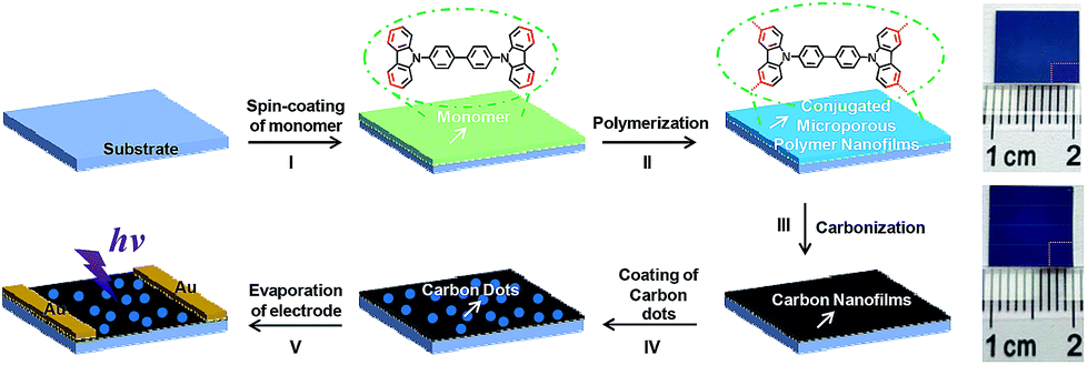 | ||
| Fig. 1 Illustration of the preparation for large-area CNFs and the fabrication of photodetector. (I) A monomer solution was spin-coated onto a pre-cleaned SiO2/Si substrate. (II) CMP nanofilms were obtained via FeCl3-catalysed surface-confined oxidative polymerization. (III) CMP nanofilms were carbonized to form CNFs under different annealing temperature. (IV) CDs were sprayed onto CNFs. (V) Evaporation of gold electrodes to prepare photodetector. The right figures are the large-area CMP nanofilm (up) and carbon nanofilm (bottom), and the bottom right corner is the bare region. | ||
The analysis of the experimental optical microscope, atomic force microscopy (AFM) and transmission electron microscope (TEM) measurements allowed us to know more about the morphologies and structures of these CMP nanofilm, CNFs and CDs. Fig. 2a shows the optical micrograph of CMP nanofilm grown on the SiO2/Si substrate. The color variation between the bare region and the CMP nanofilm covered part indicates the successful fabrication of large-area CMP nanofilm with a nanoscale thickness of ∼3.21 nm (Fig. 2b). The prepared free-standing CMP nanofilm can be transferred onto a TEM copper grid, indicating a strong chemical structure of CMP nanofilm. In the study of CNFs, CNF-750 was used as an example. It was found that the CNF maintains a continuous and perfect film state even underwent high temperature anneal (Fig. 2d and e). Compared to the CMP nanofilm, the thickness of CNF-750 was decreased from 3.21 nm to 1.20 nm (Fig. 2e), and the CNF-750 can also be transferred onto a TEM grid (Fig. 2f). In the case of CDs, the AFM image of monodispersed CD shows that the height of the obtained CDs is about 7 nm (Fig. 2h). Fig. 2i presents a TEM image of the CDs, from which the diameter of a single CD is about 15 nm. The high crystallinity of CDs is confirmed by the high-resolution TEM image with well resolved lattice fringes of 0.302 nm (Fig. S5†), which was agreed well with the spacing between graphene (002) layers.34
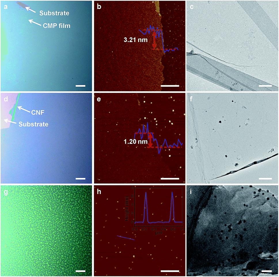 | ||
| Fig. 2 Morphology characterizations of CMP, CNF-750 and CDs. Optical micrographs of (a) CMP nanofilm, (d) CNF-750 and (g) CDs on SiO2/Si substrates. AFM images of (b) CMP nanofilm, (e) CNF-750 and (h) CDs on SiO2/Si substrates. TEM images of (c) CMP nanofilm, (f) CNF-750 and (i) CDs on TEM copper grids. Scale bars: (a, d and g) 20 μm, (b, e and h) 1 μm, (c and f) 2 μm, and (i) 100 nm. | ||
To further explore the structural transformation of CMP films before and after annealing, Raman spectra, Fourier transform infrared spectroscopy (FTIR), X-ray photoelectron spectroscopy (XPS), and ultraviolet (UV) were carried out. Two absorption peaks at 297 and 340 nm are observed for the monomer (Fig. 3a), corresponding to the π–π* electron transition of carbazole units. In comparison with monomer, CMP exhibits a broader absorption peak, suggesting an increase of conjugation length or the enhancement of intermolecular interactions of CMP.24 The new peak at 812 cm−1 from trisubstituted carbazole ring of CMP indicates the success of crosslinking reaction (Fig. S6†). The disappearance of peak area between 830 and 720 cm−1 indicates the fracture of carbazole group after the annealing process, accompanying with a large decrease of the quaternary N due to the decomposition of carbazole group and a increase of graphitic-N at 400.8 eV due to the graphitization at high temperature (Fig. S7†). In the Raman spectra of CMP nanofilm and CNFs which were annealed under low temperatures (400, 600 °C), no characteristic peaks were found, indicating the disordered nature of the thin film samples (Fig. 3b). However, with further increase of annealing temperatures to 700, 750, and 800 °C, two new peaks are observed. These peaks are referred to as the so-called D- and G-peaks, their positions, shapes, and intensities ratios (I(D)/I(G)) provide information about the degree of order in the carbon network. For instance, the CNF-750 shows D/G bands at 1353/1592 cm−1. In general, the D- and G-peaks represent the vibration modes of sp2 carbon atoms.35,36 Therefore, the intensity ratio of the disordered D-peak and the crystalline G-peak is a measurement of the disorder extent. The I(D)/I(G) ratios of CNFs annealed under 700, 750 and 800 are 0.97, 0.88, and 0.95, respectively (Fig. 3c). Even if the D/G bands do not appear under low annealing temperatures, the thicknesses of the CNFs are decreased after annealing at 400 or 600 °C. CNFs with the thicknesses from ∼3.21 to ∼1.06 nm were obtained with the increase of annealing temperature (Fig. 3d). Moreover, the surface morphologies of these as-prepared CNFs also hinge on the annealing temperatures. The root-mean-square roughness (Rrms) values of the CNFs posed inversely proportional (from 1.12 to 0.53 nm) to the increase of annealing temperatures, indicating the smoother surface CNF annealed under high temperature than its counterparts under low temperature (Fig. S8† and 3e). The two prominent peaks (D-peak at 1366 cm−1 and the G-peak at 1576 cm−1) with a I(D)/I(G) of 0.87 is observed, which is close that of graphite (0.88), indicating the similar structure of CDs and graphite (Fig. 3f).
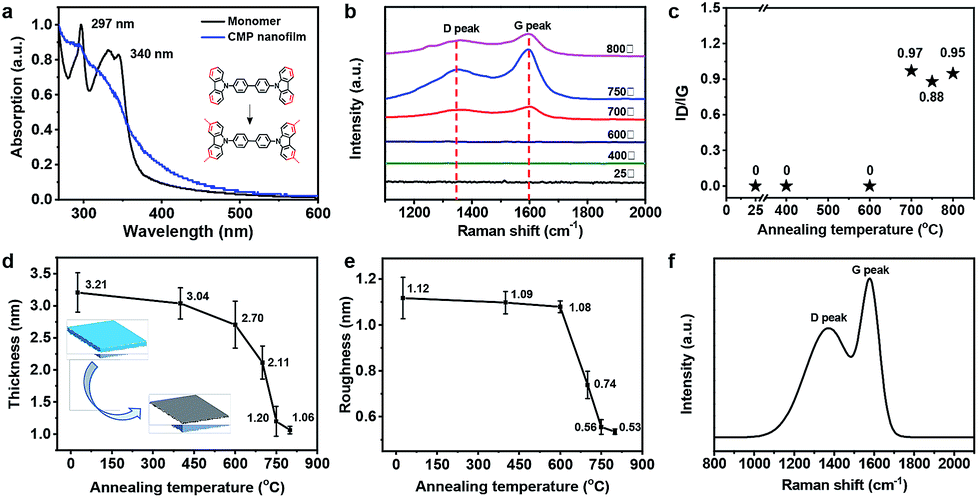 | ||
| Fig. 3 (a) Normalized UV-vis absorption spectra of monomer and CMP nanofilm on quartz plates. (b) Raman spectra of CMP nanofilm and CNFs which were annealed with different temperatures. (c) The intensity ratios (I(D)/I(G)) of CMP nanofilm and these CNFs. (d) The thicknesses and (e) surface roughness of CMP nanofilm and CNFs. (f) Raman spectra of CDs. | ||
The electrical conductivity of these CNFs with diverse anneal temperature were measured (Fig. 4a). Generally, the conductivity of CNFs increased as the annealing temperature increasing. The current–voltage (I–V) curves of CNFs annealed under low temperatures (400, 600, and 700 °C) exhibited relative low current density and high resistance underwent the identical measurements. The typical nonlinear I–V curve of CNF-750 indicated a semiconducting property, while CNF-800 exhibited a metal-like conductor property due to the typical linear I–V curve. The increase in the conductivity of CNF films probably attributed to the increase of graphitization according to our previous Raman and XPS spectra. Fig. 4b shows ID as a function of gate voltage (VG) at VDS = 3 V for the CNT-750 based transistor, the transfer characteristics indicate a typical p-type behavior with a transconductance (gm = dID/dVG) of 1.6 × 10⁻⁸ S, obtained from the linear-regime. The length of the film in the channel is 195 μm, and the width is 259 μm (Fig. S9†). The effective mobility (μ) was estimated to be 0.35 cm2 V−1 s−1 according to the previous reported equation.37
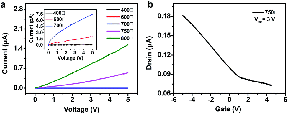 | ||
| Fig. 4 (a) The I–V curve of the CNFs as a function of annealing temperature. (b) Transfer characteristic (ID–VG) of the CNF-750 based transistor. | ||
This semiconducting property was further confirmed according to the nonlinear I–V curve in Fig. 5a. The current intensity increased slightly under the illumination of a xenon lamp, suggesting a weak photoresponsive ability of CNF-750 (the red line). Moreover, after coating with CDs, the CDs/CNF-750 heterostructure showed superior response to light compared to pure CNF-750 (Fig. 5b). The measured current increased from 1.57 to 4.71 μA under xenon lamp irradiation at a source-drain bias of 5 V without gate voltage. Moreover, the time-dependent photo-induced current measurement upon turning the xenon lamp on and off was also conducted at room temperature (Fig. 5c). After several on–off cycles, the photocurrent level exhibited negligible fluctuation, indicating the good reliability and reversibility of the photodiode. Response time is a crucial parameter for photodetectors in order to fulfill the requirements of practical applications.38 The temporal response of the CDs/CNF-750 heterostructure (Fig. 5d) demonstrated that the currents of our device rose and dropped sharply with response and decay time of 2.23 and 1.17 s, respectively, illustrating fast photoresponse processes.
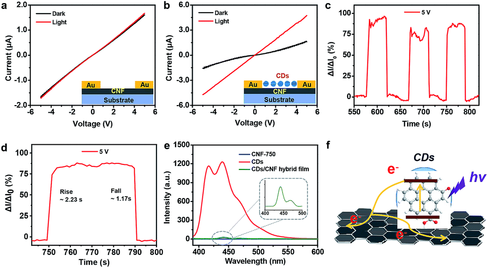 | ||
| Fig. 5 (a) The I–V characteristics of CNF based device measured in the absence and presence of light. (b) The I–V curves of CDs/CNF heterostructure based device measured with and without the light illumination. (c) Temporal photocurrent response of the CDs/CNF heterostructure based device in the dark or under light illumination. (d) Current response of CDs/CNF heterostructure photoconductor to ON/OFF illumination. (e) Photoluminescence spectra of CDs, CNF-750, and CDs/CNF-750 heterostructure. (f) A schematic illustration of the mechanism for the enhanced performance of the CDs/CNF hybrid photodetector. | ||
To understand the photoinduced charge transfer dynamics between CDs and CNF-750, the photophysical properties of CDs, CNF-750, and CDs/CNF-750 were characterized at room temperature. The peak at 287 nm was attributed to the absorption of CDs in UV region (Fig. S10†). The PL measurements of CDs, CNF-750 and CDs/CNF-750 were performed with the excitation of a 360 nm laser at room temperature. A strong blue emission from CDs was observed with a peak located at 440 nm, whereas no detectable emission was observed from CNF-750 (Fig. 5e). The fluorescence intensity of CDs was quenched for the CDs/CNF-750 hybrids, which may be result from the effective transfer of the photogenerated charges from CDs to CNF-750. This PL quenching behavior of CDs in the presence of CNF-750 is consistent with the photoresponse characterization of CDs/CNF-750, resulting in the enhanced photocurrent under light illumination.39,40 The electrons of CDs are excited to the conduction band under illumination, and the photogenerated electrons transfer to CNF-750 at the CDs/CNF-750 junction and flow through CNF-750 to Au electrode (Fig. 5f).41,42 Therefore, the recombination of photogenerated electron–hole pairs is reduced and the device photocurrent is enhanced. On the basis of aforementioned results, CDs play a crucial role in enhancing photosensitive performance of the device, which can serve as excellent UV absorbing and charge generation materials, and CNF-750 functions as a charge transporting material. Therefore, the sensing mechanism of the CDs/CNF-750 photodetector can be attributed to the charge transfer between CDs and CNF-750.
Conclusions
In summary, we have successfully prepared large-area and ultrathin carbon semiconductors converted from CMP films via in situ growth and stepwise annealing methods. By controlling the in situ growth condition and thermal annealing temperature, the carbon semiconductor has a large area up to centimeter-scale and an ultrathin nanoscale thickness of 1.06 nm at the temperature of 800 °C. Moreover, the electrical conductance of carbon films was tuned continually from low to semi- and high conductivity. A typical p-type semiconducting property was confirmed by using CNF-750 as the active channel layer in a transistor. Furthermore, by further rational constructing the all-carbon heterostructure comprising CDs and CNF-750 carbon semiconductor, the photodetector based on CDs/CNF-750 heterostructure exhibited excellent photoresponse and high repeatability at UV regime. This work provides a new way to prepare large-area and ultrathin carbon semiconductors, promoting the advances of fundamental and practical research of carbon electronics toward large-area and integrated devices.Experimental section
Fabrication of CNFs
4,4′-Di(9H-carbazol-9-yl)-1,1′-biphenyl as the monomer was dissolved in dichloromethane solvent with a concentration of 10 mg mL−1. Then the monomer solution was spin-coated (500 rpm for 2 s and 3500 rpm for 30 s) onto a clean SiO2/Si substrate, subsequently annealed in oven at 120 °C for 30 min to remove the residual solvent. The monomer covered SiO2/Si substrate was dipped in dry dichloromethane solution containing anhydrous FeCl3 for 48 h. After that, the CMP covered SiO2/Si substrate was taken out and cleaned successively with methanol, concentrated HCl and dichloromethane. Besides, patterned CMP films can be obtained by irradiating the monomer film under xenon light for 120 min with the assistance of photomasks. The carbonization process was performed by thermal annealing at different temperature (400, 600, 700, 750, and 800 °C) for 20 min under an N2 atmosphere to obtain CNFs.Synthesis of CDs
CDs were synthesized by the carbonization of citric acid (CA) through the hydrothermal method described in our previous report.43 Briefly, 1 g CA was dissolved in the solution, which contained 15 mL octadecene (ODE) with 1.5 g of hexadecylamine (HDA) treated by a hydrothermal procedure at 180 °C for 1.5 h, and then kept for 3 h. The as-synthesized CDs solution was dialyzed using a dialysis tube against deionized water for 10 days to remove unreacted ammonia and impurities.Fabrication of CDs/CNF-750 heterostructure photodetector
The CDs/CNF-750 heterostructure photodetector was fabricated onto a SiO2/Si substrate, where the CDs/CNF-750 heterostructure was chosen as the active photoresponsive layer. Firstly, the dialyzed CDs solution (200 μL) was sprayed onto CNF-750, and then heated at 100 °C for 5 min to obtain a strong contact between the CDs and CNF-750. Finally, Au electrodes (150 nm thick) were deposited through thermal evaporation using a shadow mask covered on the CDs/CNF-750 heterostructure film, and then the photodetector was fabricated.Characterization
Optical microscopy was performed using a Nikon optical microscope. The film morphologies of these CMP nanofilms and CNFs were recorded with a commercial AFM instrument (Dimension ICON with NanoScope V controller, Bruker) under ambient conditions. The TEM (HITACHI, 7605) characterizations were performed by transferring the CMP nanofilms and CNFs onto TEM grids. The absorption spectra of the monomers and polymers in film states were measured with a Shimadzu UV-3600 spectrophotometer. The fluorescence spectra were recorded on a Shimadzu RF-5301PC luminescence spectrometer. Monomer films were prepared by spin-coating monomer solution onto quartz plates. Polymer films were directly synthesized on the quartz plates. The electrical characteristics of the electronic device was characterized using a Keithley 4200-SCS semiconductor parameter analyzer. All electrical measurements were carried out under ambient conditions.Author contributions
Shang Ju designed the study, performed experiments, analyzed data, and prepared the manuscript. Yamei Ding and Shuai Chen synthesized CDs and analyzed data. Xiangjing Wang and Huiwu Mao fabricated field effect transistors. Zhe Zhou and Yuhang Yin revised the manuscript. Qing Chang performed and analyzed Raman spectroscopy. Chaoyi Ban and Mengya Song performed TEM. Juqing Liu and Zhengdong Liu supervised the study, analyzed the data and prepared the manuscript. All authors discussed the results and commented on the manuscript.Conflicts of interest
There are no conflicts to declare.Acknowledgements
We thank primary financial supports by the National Key R&D Program of China (2017YFB1002900), the National Natural Science Foundation of China (61622402, 51703093), the Natural Science Foundation of Jiangsu (BK20171000), and the Jiangsu Specially-Appointed Professor programme, the Six Talent Plan (2015XCL015).Notes and references
- F. Yang, S. Cheng, X. Zhang, X. Ren, R. Li, H. Dong and W. Hu, Adv. Mater., 2018, 30, 1702415–1702442 CrossRef PubMed.
- E. Shi, H. Li, L. Yang, J. Hou, Y. Li, L. Li, A. Cao and Y. Fang, Adv. Mater., 2015, 27, 682–688 CrossRef CAS PubMed.
- A. H. Khan, S. Ghosh, B. Pradhan, A. Dalui, L. K. Shrestha, S. Acharya and K. Ariga, Bull. Chem. Soc. Jpn., 2017, 90, 627–648 CrossRef.
- J. Di, J. Xiong, H. Li and Z. Liu, Adv. Mater., 2018, 30, 1704548 CrossRef PubMed.
- D. J. Appelhans, Z. B. Lin and M. T. Lusk, Phys. Rev. B: Condens. Matter Mater. Phys., 2010, 82, 073410–073414 CrossRef.
- K. S. Novoselov, A. K. Geim, S. V. Morozov, D. Jiang, M. I. Katsnelson, I. V. Grigorieva, S. V. Dubonos and A. A. Firsov, Nature, 2005, 438, 197–200 CrossRef CAS PubMed.
- I. Meric, M. Y. Han, A. F. Young, B. Ozyilmaz, P. Kim and K. L. Shepard, Nat. Nanotechnol., 2008, 3, 654–659 CrossRef CAS PubMed.
- S. J. Guo and S. J. Dong, Chem. Soc. Rev., 2011, 40, 2644–2672 RSC.
- M. Ammon, T. Sander and S. Maier, J. Am. Chem. Soc., 2017, 139, 12976–12984 CrossRef CAS PubMed.
- C. Moreno, M. Vilas-Varela, B. Kretz, A. Garcia-Lekue, M. V. Costache, M. Paradinas, M. Panighel, G. Ceballos, S. O. Valenzuela, D. Pena and A. Mugarza, Science, 2018, 360, 199–203 CrossRef CAS PubMed.
- X. G. Liang, Y. S. Jung, S. W. Wu, A. Ismach, D. L. Olynick, S. Cabrini and J. Bokor, Nano Lett., 2010, 10, 2454–2460 CrossRef CAS PubMed.
- J. M. Cai, C. A. Pignedoli, L. Talirz, P. Ruffieux, H. Sode, L. B. Liang, V. Meunier, R. Berger, R. J. Li, X. L. Feng, K. Mullen and R. Fasel, Nat. Nanotechnol., 2014, 9, 896–900 CrossRef CAS PubMed.
- S. Eigler and A. Hirsch, Angew. Chem., Int. Ed., 2014, 53, 7720–7738 CrossRef CAS PubMed.
- J. Baringhaus, M. Ruan, F. Edler, A. Tejeda, M. Sicot, A. Taleb-Ibrahimi, A. P. Li, Z. G. Jiang, E. H. Conrad, C. Berger, C. Tegenkamp and W. A. de Heer, Nature, 2014, 506, 349–354 CrossRef CAS PubMed.
- Z. Y. Jia, Y. J. Li, Z. C. Zuo, H. B. Liu, C. S. Huang and Y. L. Li, Acc. Chem. Res., 2017, 50, 2470–2478 CrossRef CAS PubMed.
- A. I. Cooper, Adv. Mater., 2009, 21, 1291–1295 CrossRef CAS.
- J. W. Colson and W. R. Dichtel, Nat. Chem., 2013, 5, 453–465 CrossRef CAS PubMed.
- H. Sahabudeen, H. Y. Qi, B. A. Glatz, D. Tranca, R. H. Dong, Y. Hou, T. Zhang, C. Kuttner, T. Lehnert, G. Seifert, U. Kaiser, A. Fery, Z. K. Zheng and X. L. Feng, Nat. Commun., 2016, 7, 13461–13468 CrossRef PubMed.
- P. Angelova, H. Vieker, N. E. Weber, D. Matei, O. Reimer, I. Meier, S. Kurasch, J. Biskupek, D. Lorbach, K. Wunderlich, L. Chen, A. Terfort, M. Klapper, K. Mullen, U. Kaiser, A. Golzhauser and A. Turchanin, ACS Nano, 2013, 7, 6489–6497 CrossRef CAS PubMed.
- D. Anselmetti and A. Golzhauser, Angew. Chem., Int. Ed., 2014, 53, 12300–12302 CAS.
- N. E. Weber, S. Wundrack, R. Stosch and A. Turchanin, Small, 2016, 12, 1440–1445 CrossRef CAS PubMed.
- T. Mori, H. Tanaka, A. Dalui, N. Mitoma, K. Suzuki, M. Matsumoto, N. Aggarwal, A. Patnaik, S. Acharya, L. K. Shrestha, H. Sakamoto, K. Itami and K. Ariga, Angew. Chem., Int. Ed., 2018, 57, 9679–9683 CrossRef CAS PubMed.
- J. Tan, S. Namuangruk, W. F. Kong, N. Kungwan, J. Guo and C. C. Wang, Angew. Chem., Int. Ed., 2016, 55, 13979–13984 CrossRef CAS PubMed.
- Z. D. Liu, M. Y. Song, S. Ju, X. Huang, X. J. Wang, X. T. Shi, Y. Zhu, Z. Wang, J. Chen, H. Li, Y. C. Cheng, L. H. Xie, J. Q. Liu and W. Huang, ACS Appl. Mater. Interfaces, 2018, 10, 4010–4017 CrossRef CAS PubMed.
- V. Senkovskyy, I. Senkovska and A. Kiriy, ACS Macro Lett., 2012, 1, 494–498 CrossRef CAS.
- C. Gu, Y. C. Chen, Z. B. Zhang, S. F. Xue, S. H. Sun, K. Zhang, C. M. Zhong, H. H. Zhang, Y. Y. Pan, Y. Lv, Y. Q. Yang, F. H. Li, S. B. Zhang, F. Huang and Y. G. Ma, Adv. Mater., 2013, 25, 3443–3448 CrossRef CAS PubMed.
- A. Sengupta, S. Datta, C. L. Su, T. S. Herng, J. Ding, J. J. Vittal and K. P. Loh, ACS Appl. Mater. Interfaces, 2016, 8, 16154–16159 CrossRef CAS PubMed.
- I. Salzmann, G. Heimel, M. Oehzelt, S. Winkler and N. Koch, Acc. Chem. Res., 2016, 49, 370–378 CrossRef CAS PubMed.
- Y. H. Yin, Z. D. Liu, M. Y. Song, S. Ju, X. J. Wang, Z. Zhou, H. W. Mao, Y. M. Ding, J. Q. Liu and W. Huang, J. Mater. Chem. C, 2018, 6, 11162–11169 RSC.
- Z. D. Liu, Y. H. Yin, F. Xiu, X. J. Wang, S. Ju, M. Y. Song, Q. Chang, J. Chen, J. Q. Liu and W. Huang, J. Mater. Chem. C, 2018, 6, 7295–7301 RSC.
- G. Konstantatos, M. Badioli, L. Gaudreau, J. Osmond, M. Bernechea, F. P. G. de Arquer, F. Gatti and F. H. L. Koppens, Nat. Nanotechnol., 2012, 7, 363–368 CrossRef CAS PubMed.
- W. B. Niu, H. Chen, R. Chen, J. F. Huang, A. Palaniappan, H. D. Sun, B. G. Liedberg and A. I. Y. Tok, Small, 2014, 10, 3637–3643 CrossRef CAS PubMed.
- Z. H. Sun, Z. K. Liu, J. H. Li, G. A. Tai, S. P. Lau and F. Yan, Adv. Mater., 2012, 24, 5878–5883 CrossRef CAS PubMed.
- W. J. Niu, R. H. Zhu, Yan-Hua, H. B. Zeng, S. Cosnier, X. J. Zhang and D. Shan, Carbon, 2016, 109, 402–410 CrossRef CAS.
- A. C. Ferrari and J. Robertson, Phys. Rev. B: Condens. Matter Mater. Phys., 2001, 64, 075414–075427 CrossRef.
- A. Turchanin, A. Beyer, C. T. Nottbohm, X. H. Zhang, R. Stosch, A. Sologubenko, J. Mayer, P. Hinze, T. Weimann and A. Golzhauser, Adv. Mater., 2009, 21, 1233–1237 CrossRef CAS.
- Z. Jin, J. Yao and C. Kittrell, et al., ACS Nano, 2011, 5, 4112–4117 CrossRef CAS PubMed.
- Z. Zhou, Y. M. Ding, H. Y. Ma, L. J. Cao, X. Wang, X. Huang, J. Q. Liu and W. Huang, APL Mater., 2019, 7, 031501–031506 CrossRef.
- T. V. Tam, S. H. Hur, J. S. Chung and W. M. Choi, Sens. Actuators, A, 2015, 233, 368–373 CrossRef CAS.
- D. T. Thanh, K. B. Ko, Z. Khurelbaatar, C. J. Choi, C. H. Hong and T. V. Cuong, Mater. Res. Bull., 2017, 91, 49–53 CrossRef CAS.
- Z. H. Sun and H. X. Chang, ACS Nano, 2014, 8, 4133–4156 CrossRef CAS PubMed.
- D. A. Nguyen, H. M. Oh, N. T. Duong, S. Bang, S. J. Yoon and M. Seok Jeong, ACS Appl. Mater. Interfaces, 2018, 10, 10322–10329 CrossRef CAS PubMed.
- Y. M. Ding, Q. Chang, F. Xiu, Y. Y. Chen, Z. D. Liu, C. Y. Ban, S. Cheng, J. Q. Liu and W. Huang, Nanoscale, 2018, 10, 4189–4193 RSC.
Footnote |
| † Electronic supplementary information (ESI) available. See DOI: 10.1039/c9ra03052b |
| This journal is © The Royal Society of Chemistry 2019 |