
 Open Access Article
 This Open Access Article is licensed under a
 Creative Commons Attribution 3.0 Unported Licence
High absorption shielding material of poly(phthalazinone etherketone)/multiwall carbon nanotube composite films with sandwich configurations†
Yunping Hua,
Ping Tanga,
Longwei Lia,
Junyu Yangb,
Xigao Jian a and
Yuezhen Bin*a
a and
Yuezhen Bin*a
aDepartment of Polymer Science and Engineering, Faculty of Chemical, Environmental and Biological Science and Technology, Dalian University of Technology, No. 2 Linggong Rd, Dalian, 116024, P. R. China. E-mail: binyz@dlut.edu.cn; Fax: +0411-84986093; Tel: +0411-84986093
bDepartment of Chemical Engineering, University of Pittsburgh, 4200 Fifth Avenue, Pittsburgh, PA 15260, USA
First published on 14th June 2019
Abstract
Sandwich structure can be induced to achieve excellent electromagnetic interference shielding effectiveness (EMI SE) as is well known. However, how to optimize the structure to achieve performance optimization is still a problem. Herein, a poly(phthalazinone etherketone)/multiwall carbon nanotube (PPEK/MWCNT) composite with homodisperse and high content (15 wt%) of MWCNT was prepared by a water induced phase separation process. A sandwich structure was designed by introducing a wave-transmitting layer between the PPEK/MWCNT composite films. The MWCNT loading of the shielding layer and the wave-transmitting layer thickness (d) were varied to systematically investigate their influence on shielding performance in the X-band (8.2–12.4 GHz). EMI SE shows strong d value dependence. When the shielding layer was fixed, EMI SE showed a trend of decreasing, rising, leveling off and then decreasing again with d value increasing. The d value in the leveling off stage is the best value for performance optimization. The best d value decreased with increasing MWCNT content of the shielding layer. An absorption dominated SE up to 65 dB and a high increment rate of 140% of SE were achieved by optimization of the d value and shielding layer.
1 Introduction
Nowadays, the abuse of electronic device causes serious electromagnetic pollution, which has become one of the serious pollutions coming just after water pollution, air pollution and noise pollution. High-energy electromagnetic radiation may disturb the normal operation of electronic equipment, shorten the life of the equipment, result in the leakage of information and affect human health.1–3 Consequently, the development of materials that can act as microwave absorbers or shields against electromagnetic waves especially in the X-band has become essential.4–6 The electromagnetic interference shielding effectiveness (EMI SE) of shielding materials depends on the synergistic effect of EMI absorption, reflection and multiple reflection. Shielding performance can be enhanced by increasing the intrinsic EMI SE of shielding materials through improving electrical conductivity, magnetic permeability and thickness of shielding materials. However, designing a special structure is a simpler and more feasible way to improve shielding performance. Unfortunately, how to optimize the structure to achieve performance optimization is still a problem.Metal sheets and resin-based metal micro-nanoparticle composites have been widely used to process into high-performance EMI shielding materials because of their excellent reflection property. But the application of metal materials is limited by their high density, poor processability and dispersibility.2,3,7 Moreover, secondary pollution caused by reflected electromagnetic waves is also a fatal limitation. Besides the conventional metal-based EMI shielding materials, resin matrix composites containing carbon-based nanofillers, particularly carbon nanotube (CNT)8–10 and graphene11,12 have become the focus of research due to their advantages of light weight, excellent processability, resistance to corrosion, and broad absorption bandwidth.13–18
CNTs are nano-scale hollow tubes with large L/D ratio. It has extraordinary electrical, thermal, mechanical properties and excellent absorbing properties. CNTs filled composites may be fit for new shielding materials with lightweight, broadband and high absorption efficiency. CNTs can be added directly into resin as fillers during preparation of composites.19–22 The compatibility between resin and CNTs can be improved by surface modification of CNTs to improve the dispersity at high filling levels.23 The lightweight CNT composites can be prepared by mechanical mixing easily, but the SE value of the composites is not high. Y. Huang, et al. prepared a type of single-walled carbon nanotube/epoxy composites of 2 mm thick showing an SE of only 20–30 dB with a high filler content of 15 wt%.21 Increasing the filling loading and its dispersity in resin is still key issue for obtaining a high SE value. In addition, for the applications in special fields, where the materials require not only excellent shielding performance but also superior thermal stability and excellent mechanical properties, high performance plastics rather than general plastics are demanded. Poly(phthalazinone etherketone) (PPEK) is a new type of amorphous polymer with the relatively high heat-resistance up to 400 °C and Tg higher than 250 °C.24 In addition, the twisty and non-coplanar structure of phthalazinone moieties of its molecular chain endows it a better solubility in chloroform and N-methyl-pyrrolidone (NMP) and some other organic solvents.25,26 In view of its superior performance, PPEK can be easily processed and applied in a variety of fields as high performance plastic and composite.
Taking the above factors into consideration, special structures have been induced to achieve excellent electromagnetic shielding performance, such as sandwich structure,19,20,27–29 gradient structure,19,29 porous structure30,31 and so on. The study of Jin Gyu Park, et al. showed that the composite laminated structures made with CNT bulkypaper (BP) and epoxy or polyethylene insulating layer can increase the EMI SE from 45 dB to close to 100 dB owing to the utilization of the double-shielding effect.27 Li Y., et al. introduced a wave-transmitting layer (pure polyurethane layer) between two pieces of polyurethane/graphene (PUG) foams to prepare a sandwich structure, by which the SE of the samples could be dramatically enhanced.29
Plastic matrix nanocomposite was prepared for the application in EMI shielding in many reports. Sandwich structure has been induced to achieve excellent EMI SE as reported in a few reports.19,20,27–29 However, how to optimize the structural to achieve performance optimization has not been thoroughly explored till date. Some investigation needs to be done to explore what factors affect the shielding property and how these factors affect shielding property. In this paper, PPEK and multiwall carbon nanotubes composite films (PPEK/MWCNT) were prepared as shielding layers with the aid of water induced phase separation (WIPS) process. A series of sandwich structure were designed by changing shielding layer and wave-transmitting layer. EMI SE dependence on the wave-transmitting layer thickness (d) and shielding layer SE was investigated in details.
2 Experimental
2.1 Materials
MWCNT (diameter: 10–20 nm, length: 10–30 μm) were procured from Chengdu Organic Chemicals CO., Ltd. Poly(phthalazinone etherketone) (PPEK) with a molecular weight of 70![[thin space (1/6-em)]](https://www.rsc.org/images/entities/char_2009.gif) 000 was supplied by Dalian BaoLiMo New Materials Co., Ltd. PPEK powder was purified using chloroform. Anhydrous ethanol (AR), chloroform (AR) and 1-methyl-2-pyrrolidinone (NMP, AR) were purchased from LiaoDong Chemical Reagent (China).
000 was supplied by Dalian BaoLiMo New Materials Co., Ltd. PPEK powder was purified using chloroform. Anhydrous ethanol (AR), chloroform (AR) and 1-methyl-2-pyrrolidinone (NMP, AR) were purchased from LiaoDong Chemical Reagent (China).
2.2 Sample preparation
The preparation procedure is illustrated in Fig. 1. At first PPEK/MWCNT composite films were prepared using WIPS technique. Then sandwich structure was designed by using two sheets of composite films as shielding layers and a pure PPEK resin sheet as wave-transmitting layer.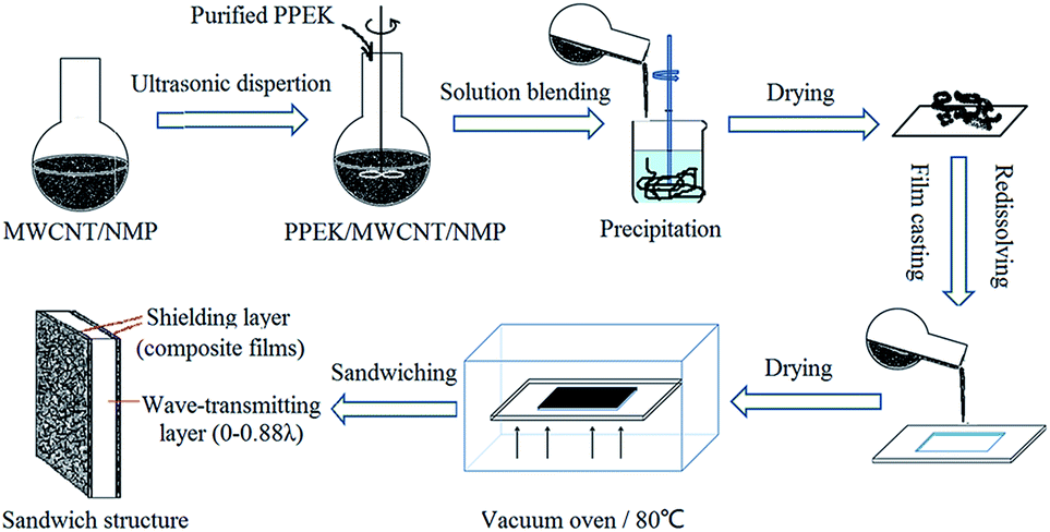 | ||
| Fig. 1 Preparation of composite film with WIPS method and sandwich structure of shielding materials. | ||
The above PPEK/MWCNT (15 wt%) master batch was used for preparing PPEK/MWCNT composite film with 1–10 wt% CNT contents. A certain amount of PPEK/MWCNT master batch and purified PPEK were added to NMP solvent. By adjusting the mass ratio of PPEK/MWCNT master batch and PPEK the samples containing 1, 2, 3, 5, 10 and 15 wt% of MWCNTs were denoted as CNT1, CNT2, CNT3, CNT5, CNT10 and CNT15 respectively. The above mixtures were mechanically stirred at 80 °C for 2 h to obtain uniform mixing solutions. The solutions were casted on a self-made glass mold and dried at 80 °C in vacuum for 9 h to form composite films. The film thickness was designed as 100 or 200 μm. PPEK/MWCNT composite film with CNT loading of 5 wt% and thickness of 100 μm was named as CNT5-100. Others were named in the same way. The composite films are used as shielding layers to fabricating the sandwich structure in the following experiment.
2.3 Characterization
Cross-sectional morphology of composite film was observed by field emission scanning electron microscopy (NOVA Nano SEM 450). The fractured surfaces of samples were stuck onto the SEM holder followed by spraying gold for 30 s. The electrical resistance of composite films was measured by two-point probe method. Rectangular test samples (1 cm × 3 cm) were coated with a thin layer of conductive silver paste at the end, and then tested with HP4339B high resistance tester (R > 107 Ω) and R6441A digital multimeter (R < 107 Ω). The EMI shielding performance was characterized by waveguide measurement system using a vector network analyzer (3656D, The 41st Institute of China Electronics Technology Group Corporation) in the frequency range of 8.2–12.4 GHz (Fig. S1†). The samples were cut into a rectangular shape to fit in well with the chamber of the sample holder. The four main scattering parameters, S11, S12, S21 and S22 were detected.The incident electromagnetic wave passing through a material undergoes four different processes: reflection, absorption, penetration and multiple reflection.32,33 The EMI shielding effectiveness (SE) should be the sum of its reflection energy and internal absorption energy. SER, SEA and EMI SE were analyzed by the following equations23,34,35 based on the values of S11, S12, S21 and S22:
| R = |S11|2 = |S22|2 | (1) |
| T = |S12|2 = |S21|2 | (2) |
| A = 1 − R − T | (3) |
|
SER = 10log(1/(1 − R))
| (4) |
|
SEA = 10log((1 − R)/T)
| (5) |
| SE = SEA + SER | (6) |
3 Results and discussion
3.1 Morphology and electrical properties of PPEK/MWCNT composite films
The morphology of PPEK/MWCNT composite films is showed in Fig. 2. MWCNTs can be uniformly dispersed in composite even at a high loading of 15 wt%. In addition, MWCNTs are overlapped with each other to form a conductive path. The WIPS method has a great advantage over the conventional melt-compounding method for making good filler dispersion especially at high filler loading. Generally, high loading of nanofillers in polymer matrix during compounding process tends to give an obvious increase in melt viscosity due to the extremely high specific surface area of nanofillers. In the present experiment, at first a large amount of MWCNTs were added into PPEK solution at a low concentration and then the PPEK/MWCNT nanocomposite was obtained by precipitation through the WIPS process. This WIPS method can effectively avoid serious processing problems caused by high viscosity of the mixture.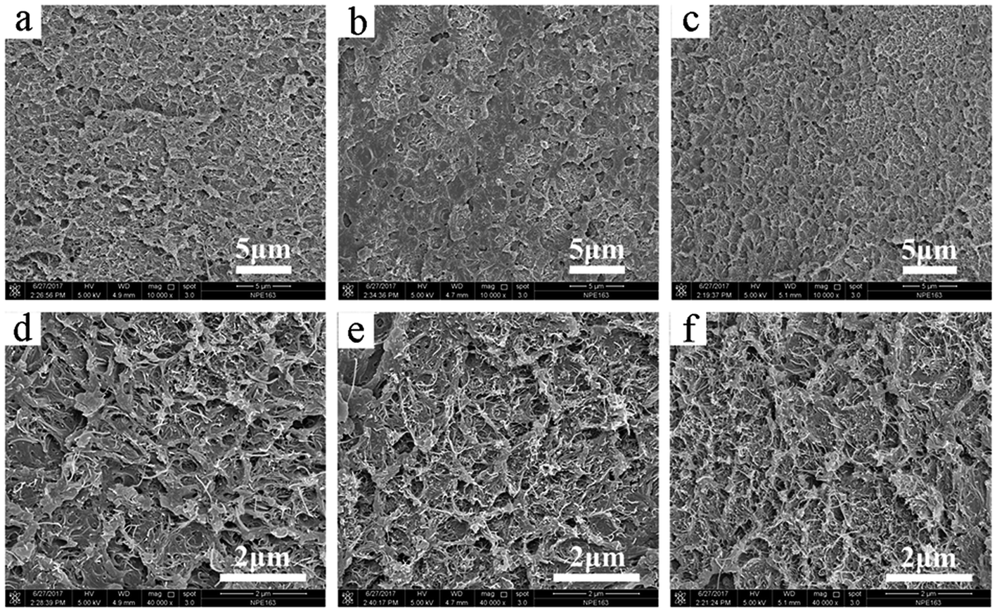 | ||
| Fig. 2 SEM micrographs of the fractured surfaces of PPEK/MWCNT composite films with MWCNT loading of: (a and d) 5 wt%, (b and e) 10 wt% and (c and f) 15 wt%. | ||
The EMI shielding performance of conductive composites is closely related to their electrical properties.27,36–38 The electrical conductivity of PPEK/MWCNT composite films was studied. Fig. 3 shows the nonlinear relationship between the logarithms of electrical conductivity of PPEK/MWCNT composite films and MWCNT mass fraction. The conductivity of composite film with 1 wt% loading of MWCNT was 10−12 S cm−1 level. Then the electrical conductivity reached 6 × 10⁻⁴ S cm−1 when the content of MWCNT increased to 2 wt%, indicating the formation of conductive networks and up to the percolation threshold. As further increase in MWCNT loading, the growth trend of conductivity became gentle. On the whole, the conductivity of the PPEK/MWCNT composite films displays a great promotion over 13 orders of magnitude as MWCNT content higher than 5 wt% and reached 0.39 S cm−1 at 15 wt% of MWCNTs. As shown in the inset of Fig. 3, the relationship of the electrical conductivity and the MWCNT loading of PPEK/MWCNT composites was evaluated with power-law equation,4,39 i.e. σ = σ0(p − pc)t. In the formula, σ represents the electrical conductivity of PPEK/MWCNT composites, σ0 is a constant related to conductivity of fillers, p is the volume fraction of fillers, and pc is the percolation threshold. t value can be used to judge the dimensionality of the conductive system. The low pc of 1.24 vol% results from the uniform dispersion of MWCNTs, and the obtained t is 2.26, confirming the formation of 3D conductive networks. The increase of MWCNT content also makes for improving thermal stability (Fig. S2 and Table S1; ESI†) and mechanical property (Fig. S3; ESI†) of composite films.
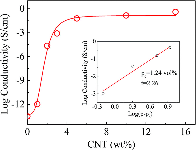 | ||
| Fig. 3 The logarithm of electrical conductivity of PPEK/MWCNT composite films with different MWCNT loading. The inset is the log–log plot of conductivity versus (p − pc) and the solid line is a fit to the measured data using power-law equation, i.e. σ = σ0(p − pc)t. | ||
3.2 EMI shielding performance of composite film and its sandwich structure in X-band
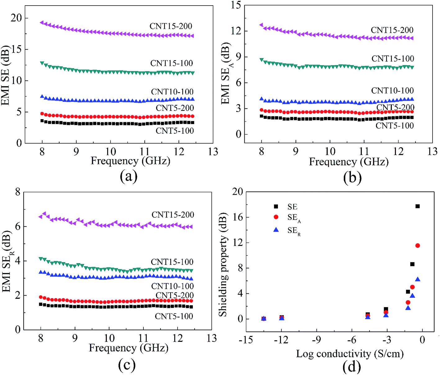 | ||
| Fig. 4 (a) EMI SE, (b) SEA and (c) SER versus frequency for PPEK/MWCNT composite films in X-band; (d) variation in the value of SE, SEA and SER with electrical conductivity of PPEK/MWCNT composite films (200 μm). | ||
The low electrical conductivity of PPEK/MWCNT composite films with filler loading less than 3 wt% induced almost no EMI shielding which was not shown here. As increasing filler content, the EMI SE of CNT5-100 is about 3 dB, and CNT15-100 increases to 12 dB (>90% attenuation). CNT15-200 reveals a shielding effectiveness of nearly 20 dB, and the SE is almost independent of frequency change in the X-band.
For further investigation of the shielding mechanism, SE for PPEK/MWCNT composites is resolved into resultant SEA and SER components as shown in Fig. 4b and c, respectively. The result shows that SER increases with increase in MWCNTs loading because of increase in electrical conductivity of the composites (Fig. 4d). However, with increasing of MWCNT content, SEA increases more rapidly compared to corresponding SER component. Such a behavior is direct consequence of square root and logarithmic dependence of SEA and SER on conductivity respectively.40,41
When the content of MWCNT is more than 15 wt%, it is difficult for MWCNT to disperse in PPEK uniformly due to plenty of entanglements, thus the improvement of EMI shielding performance is limited. In this case, increasing the thickness of shielding materials or designing special structure is a more effective way to enhance the shielding performance.
| G = (SEmax − SE0)/SE0 × 100% | (7) |
Fig. 5 shows the EMI SE of sample A with two shield layers (CNT5-100) and a wave-transmitting resin sheet (d = 0–22 mm). While d < 4 mm, the SE decreases as d value increasing. But further increasing in d value, EMI SE increased. Even though, the maximum SE is less than 10 dB which is too low to meet the request for commercial utilization. The resonance peak where shielding performance descended dramatically appeared while d > 0.56λ (14 mm). The resonance peak appeared at f > 12.40 GHz (d = 16 mm, 0.64λ) and f = 10.45 GHz (d = 22 mm, 0.88λ).
 | ||
| Fig. 5 The plot of SE for the sample A with different d values in the frequency of 8.2–12.4 GHz. The annotations in the figure represent the d and the unit is millimeter. | ||
The same experiment and analysis were carried out for other four series of samples B, C, D and E. To shorten the paper, the corresponding detailed results (SE, A, R, etc.) were shown as Fig. S4–S7 in ESI† respectively. The SE test result of sample E was shown in Fig. 6.
 | ||
| Fig. 6 The SE, SEA and SER of sample E with different d value in X-band. The annotations in the figure represent the d value and the unit is millimeters. | ||
Here in, we take sample E (Fig. 6 and S7, ESI†) to systematically illuminate the influence of wave-transmitting layer on shielding properties of sandwich structure by analyzing its SE, A, R, etc.
The SE of sample E increases monotonically with increasing of the d (Fig. 6a). And the increase in SE stopped at 0.32λ (8 mm) as a result of the limitation of SER and multiple SER.27 Sample E can achieve an initial SEA of 16 dB (average value) while a SER of only 8.5 dB. When the SEA reached as high as 33 dB (d = 0.32λ, 8 mm), the SER still remained only about 6.6 dB. Thus the shielding material exhibits an improved SE coupled with an absorption dominating shielding mechanism, which is different from the previously reported reflection dominated polymer/graphene and polymer/CNT nanocomposites.38,42,43 Moreover, the obtained SE (ca. 40 dB) is greater than three-layered PUG composites with higher graphene loading (16 wt%) and much thicker shielding layer (2.4 mm).29 Sandwich structure of graphene paper/wax/graphene paper28 also presents a lower SE in most frequency bands than sample E due to its thin wax layer. The amplitude of the reflected electromagnetic waves depends on impedance matching degree between the shielding material and resin. CNT15-200 is a good conductive material with much lower impedance than resin, so it shows a higher impedance mismatch and greater reflection coefficient R (Fig. S7e†). The incident microwaves can be reflected and scattered many times at the interface between MWCNT and resin, and the microwaves were difficult to escape from the system until being absorbed and converted into heat.44,45 Thus the electromagnetic waves can be attenuated in form of absorption effectively, while the corresponding SER is greatly suppressed because of the constructive interference.28 The results are consistent with those in Fig. S6,† and can be demonstrated by the decrease of reflection coefficient R and increase of absorption coefficient A (Fig. S6e and S7e, ESI†).
As further increase in d value (d > 0.4λ, 10 mm), resonance peak appeared in X-band range. This phenomenon indicates that the increase of SE caused by increasing the d value is contributed by the constructive interference.28,29 In a typical Fabry–Pérot cavity, multiple reflection waves can be aligned between parallel reflecting planes, producing constructive interference when the reflected waves are in phase.28 Resonance peak is observed when the d does not match well with the distance for the occurrence of constructive interference. This phenomenon results in a decrease of absorption coefficient A and an increase of transmission coefficient T at the same time (Fig. S7f, ESI†). It gives a good explanation to the dramatic descending of SE, SEA and the slight increase of SER.
There is a strong correlation between the SE of sandwich structure and shielding layer. To achieve desired shielding level, some investigation needs to be done to find out and alleviate the constraints. After analyzing the Fig. 5 and S4–S7 (ESI†), the d value dependence of the EMI SE was described in Fig. 7 for these sandwich samples. The SE at 8.2 GHz, 10.2 GHz and 12.4 GHz, and average SE in X-band before the appearance of resonance peak were presented in Fig. 7 respectively. In addition, the SE0, SEmax and the increment rate G of EMI SE were shown in Fig. 8. The center frequency of resonance peaks of these sandwich structures were listed in Table S2 (ESI†).
 | ||
| Fig. 7 Dependence of EMI SE on d value of sandwiched samples at frequency of: (a) 8.2 GHz, (b) 10.2 GHz and (c) 12.4 GHz; (d) average SE before the appearance of resonance peak in X-band. | ||
 | ||
| Fig. 8 (a) Initial and maximum EMI SE, SE0 and SEmax, of sample A, B, C, D and E; (b) the increment rate G of EMI SE. | ||
As shown in Fig. 7, the EMI SE of five samples show a tendency as E > D > C > B > A with the same d value at the same frequency. This is closely related to the filler content and thickness of shielding layer.
The SE of sample A, B, C and D shows the same tendency with the variation of d value. With the d increasing, the SE decreased firstly (decrease stage), then showed an upward tendency (rising stage) until reaching a plateau, and finally descended (re-decreasing stage) at some frequency band. As explained in Fig. 7, in the first stage the SE decreased resulting from the mismatch between the d and the distance of forming constructive interference. The d value range in the first stage of sample B (d < 4 mm), C (d < 2 mm) and D (d < 1.5 mm) decreases in turn. There is no descending in SE for sample E even at very small d value.
In the second stage, the EMI SE increased as increasing of d value. SE reached the maximum value when the d values are 0.56λ (14 mm), 0.48λ (12 mm), 0.4λ (10 mm), 0.32λ (8 mm) and 0.32λ (8 mm) for sample A, B, C, D and E respectively. It is interesting to note that the difference between d values is approximately 0.32λ for achieving the maximum and the lowest SE for each sandwich structure. Fig. 8 shows SE0, SEmax and the G for five series of samples. The G for sample E was up to 70.2% and the SEmax reached to 42 dB. However the SE of sample A, B, C and D is still lower than the commercial level of 30 dB even though introducing a large wave-transmitting layer. Clearly, a higher intrinsic SE of shielding layer makes for decreasing optimal d value and increasing the increment rate G of the sandwich structure.
With further increase in d value, SE decreased due to that the resonance peak appears. Table S2 (ESI†) shows that the resonance peak shifted to lower frequency at larger d, which is consistent with the phenomenon reported by Li Y.29 The shifting is due to that longer wavelengths are required by the constructive interference occurring in larger distances. Fig. S8 (ESI†) depicts the dependence of EMI SE on frequency of sandwiched samples at specific d values, 0.56λ, 0.64λ and 0.88λ. The resonance peak goes to lower frequency with the intrinsic SE of shielding layer increasing at specific d value. Moreover, the width of resonance peak becomes narrower as shown in Fig. S8c (ESI†).
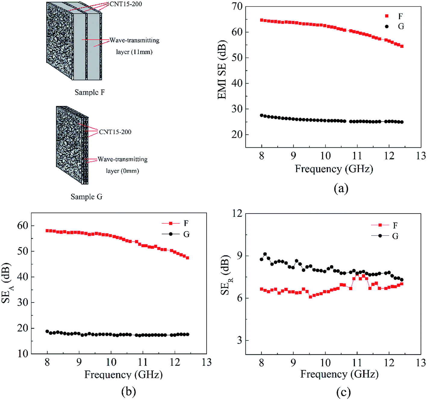
Afterwards, three pieces of shielding layers were used for preparing a sandwiched shielding material with or without wave-transmitting layer to further investigate the influence of wave-transmitting layer on the SE. Denotation of sandwiched and triple-layer composites are shown in Table S3 (ESI†). Sample F is a sample prepared by sandwiching two wave-transmitting layers of 11 mm thick among three pieces of CNT15-200. A triple-layered composite, sample G, was prepared by stacking three pieces of CNT15-200 face to face without wave-transmitting layer.
The EMI shielding performance of sample F and G are shown in Fig. 9. Sample F has an average SE of 61.5 dB in frequency range of 8.2–12.4 GHz which is much higher than that of sample G (25.7 dB). Furthermore, the improvement of the SE mainly ascribed to the increase of SEA (Fig. 9b). Given from the appropriate thickness of wave-transmitting layer, the SE of sample F is even higher than sandwich structure of BP/PE layer.27 Notably, the SE of the sandwich structure with two wave-transmitting layers (sample F) increased by 140% compared to that of multilayer structure (triple-layered sample G) with the same components of PPEK/MWCNT composite films. By contrast, the SE of sandwiched shielding material with one wave-transmitting layer (sample E) increases only by 70.2% compared to corresponding SE0 (Fig. 8). Based on this, we speculate that increasing wave-transmitting layer with best d value is beneficial to increase the increment rate of SE.
 | ||
| Fig. 9 Plots of (a) EMI SE, (b) SEA and (c) SER versus frequency for sample G and sample F in the X-band. | ||
4 Conclusion
PPEK/MWCNT composite films with homodisperse of MWCNT were prepared with the aid of WIPS process. The EMI shielding performance of composite films was evaluated in X-band. Sandwich structures were designed by sandwiching a pure resin sheet as a wave-transmitting layer to systematically investigate the influence of wave-transmitting layer and shielding layer on shielding properties by comparing their SE, A, R, etc. With the d increasing, the SE of sandwich structure decreased firstly, then upward reached a plateau, and then descended at some frequency band corresponding to the appearance of resonance peaks. The intrinsic SE of the shielding layer was negatively correlative to the best d value, while positively correlative to the increment rate G of the SE. However, it is interesting to note that the d value interval of the rising stage is almost constant, ca. 0.32λ. An absorption dominated SE up to 65 dB and high increment rate of 140% can be achieved by optimization of d value and shielding layer.Conflicts of interest
There are no conflicts of interest to declare.Acknowledgements
The authors gratefully acknowledge financial support from the National Natural Science Foundation of China (No. 21374014 and No. U1663226).Notes and references
- F. Shahzad, M. Alhabeb, C. B. Hatter, B. Anasori, S. Man Hong, C. M. Koo and Y. Gogotsi, Science, 2016, 353, 1137–1140 CrossRef CAS PubMed.
- Z. Chen, C. Xu, C. Ma, W. Ren and H. M. Cheng, Adv. Mater., 2013, 25, 1296–1300 CrossRef CAS PubMed.
- J. Liu, H. B. Zhang, R. Sun, Y. Liu, Z. Liu, A. Zhou and Z. Z. Yu, Adv. Mater., 2017, 29, 1702367 CrossRef PubMed.
- L.-C. Jia, D.-X. Yan, C.-H. Cui, X. Jiang, X. Ji and Z.-M. Li, J. Mater. Chem. C, 2015, 3, 9369–9378 RSC.
- A. P. Singh, P. Garg, F. Alam, K. Singh, R. B. Mathur, R. P. Tandon, A. Chandra and S. K. Dhawan, Carbon, 2012, 50, 3868–3875 CrossRef CAS.
- P. C. P. Watts, W. K. Hsu, A. Barnes and B. Chambers, Adv. Mater., 2003, 15, 600–603 CrossRef CAS.
- J. J. Ma, K. Wang and M. S. Zhan, RSC Adv., 2015, 5, 65283–65296 RSC.
- Z. P. Wu, T. Liu, D. M. Chen, G. Wu, Q. H. Wang, Y. H. Yin, Y. S. Li, Q. F. Xu and A. Krishamurthy, RSC Adv., 2016, 6, 62485–62490 RSC.
- L. Xu, L.-C. Jia, D.-X. Yan, P.-G. Ren, J.-Z. Xu and Z.-M. Li, RSC Adv., 2018, 8, 8849–8855 RSC.
- Y. Kato, M. Horibe, S. Ata, T. Yamada and K. Hata, RSC Adv., 2017, 7, 10841–10847 RSC.
- G. George, S. M. Simon, P. V. Prakashan, S. M. Sajna, M. Faisal, R. Wilson, A. Chandran, P. R. Biju, C. Joseph and N. V. Unnikrishnan, RSC Adv., 2018, 8, 30412–30428 RSC.
- M. Verma, P. Verma, S. K. Dhawan and V. Choudhary, RSC Adv., 2015, 5, 97349–97358 RSC.
- B. Shen, W. T. Zhai and W. G. Zheng, Adv. Funct. Mater., 2014, 24, 4542–4548 CrossRef CAS.
- D. X. Yan, H. Pang, B. Li, R. Vajtai, L. Xu, P. G. Ren, J. H. Wang and Z. M. Li, Adv. Funct. Mater., 2015, 25, 559–566 CrossRef CAS.
- D. D. L. Chung, Carbon, 2012, 50, 3342–3353 CrossRef CAS.
- S. Geetha, K. K. S. Kumar, C. R. K. Rao, M. Vijayan and D. C. Trivedi, J. Appl. Polym. Sci., 2009, 112, 2073–2086 CrossRef CAS.
- M. S. Cao, X. X. Wang, W. Q. Cao and J. Yuan, J. Mater. Chem. C, 2015, 3, 6589–6599 RSC.
- B. Zhao, C. Zhao, R. Li, S. M. Hamidinejad and C. B. Park, ACS Appl. Mater. Interfaces, 2017, 9, 20873–20884 CrossRef CAS PubMed.
- J. H. Lin, Z. I. Lin, Y. J. Pan, C. L. Huang, C. K. Chen and C. W. Lou, Composites, Part B, 2016, 89, 424–431 CrossRef CAS.
- Y. J. Liu, D. Song, C. X. Wu and J. S. Leng, Composites, Part B, 2014, 63, 34–40 CrossRef CAS.
- Y. Huang, N. Li, Y. F. Ma, D. Feng, F. F. Li, X. B. He, X. Lin, H. J. Gao and Y. S. Chen, Carbon, 2007, 45, 1614–1621 CrossRef CAS.
- Y. Chen, H. B. Zhang, Y. B. Yang, M. Wang, A. Y. Cao and Z. Z. Yu, Adv. Funct. Mater., 2016, 26, 447–455 CrossRef CAS.
- T. K. Gupta, B. P. Singh, S. R. Dhakate, V. N. Singh and R. B. Mathur, J. Mater. Chem. A, 2013, 1, 9138–9149 RSC.
- Y. Z. Meng, A. R. Hlil and A. S. Hay, J. Polym. Sci., Part A: Polym. Chem., 1999, 37, 1781–1788 CrossRef CAS.
- C. Lu, P. Chen, J. F. Li and Y. J. Zhang, Polymer, 2006, 47, 915–921 CrossRef CAS.
- G. Wang, H. Zhang, B. Q. Qian, J. Y. Wang, X. G. Jian and J. S. Qiu, Appl. Surf. Sci., 2015, 351, 169–174 CrossRef CAS.
- J. G. Park, J. Louis, Q. Cheng, J. Bao, J. Smithyman, R. Liang, B. Wang, C. Zhang, J. S. Brooks, L. Kramer, P. Fanchasis and D. Dorough, Nanotechnology, 2009, 20, 415702 CrossRef PubMed.
- W. L. Song, L. Z. Fan, M. S. Cao, M. M. Lu, C. Y. Wang, J. Wang, T. T. Chen, Y. Li, Z. L. Hou, J. Liu and Y. P. Sun, J. Mater. Chem. C, 2014, 2, 5057–5064 RSC.
- Y. Li, B. Shen, D. Yi, L. H. Zhang, W. T. Zhai, X. C. Wei and W. G. Zheng, Compos. Sci. Technol., 2017, 138, 209–216 CrossRef CAS.
- P. R. Agarwal, R. Kumar, S. Kumari and S. R. Dhakate, RSC Adv., 2016, 6, 100713–100722 RSC.
- R. Kumar, S. R. Dhakate, P. Saini and R. B. Mathur, RSC Adv., 2013, 3, 4145–4151 RSC.
- Y. Yang, M. C. Gupta, K. L. Dudley and R. W. Lawrence, Nano Lett., 2005, 5, 2131–2134 CrossRef CAS PubMed.
- R. Kitaura, N. Imazu, K. Kobayashi and H. Shinohara, Nano Lett., 2008, 8, 693–699 CrossRef CAS PubMed.
- K. Singh, A. Ohlan, V. H. Pham, R. Balasubramaniyan, S. Varshney, J. Jang, S. H. Hur, W. M. Choi, M. Kumar, S. K. Dhawan, B. S. Kong and J. S. Chung, Nanoscale, 2013, 5, 2411–2420 RSC.
- A. Ohlan, K. Singh, A. Chandra and S. K. Dhawan, Appl. Phys. Lett., 2008, 93, 053114 CrossRef.
- J. J. Liang, Y. Wang, Y. Huang, Y. F. Ma, Z. F. Liu, J. M. Cai, C. D. Zhang, H. J. Gao and Y. S. Chen, Carbon, 2009, 47, 922–925 CrossRef CAS.
- H. B. Zhang, W. G. Zheng, Q. Yan, Z. G. Jiang and Z. Z. Yu, Carbon, 2012, 50, 5117–5125 CrossRef CAS.
- N. Li, Y. Huang, F. Du, X. He, X. Lin, H. Gao, Y. Ma, F. Li, Y. Chen and P. C. Eklund, Nano Lett., 2006, 6, 1141–1145 CrossRef CAS PubMed.
- F. Ren, Z. Li, L. Xu, Z. Sun, P. Ren, D. Yan and Z. Li, Composites, Part B, 2018, 155, 405–413 CrossRef CAS.
- P. Saini, V. Choudhary, B. P. Singh, R. B. Mathur and S. K. Dhawan, Synth. Met., 2011, 161, 1522–1526 CrossRef CAS.
- B. P. Singh, P. Prabha, P. Saini, T. Gupta, P. Garg, G. Kumar, I. Pande, S. Pande, R. K. Seth, S. K. Dhawan and R. B. Mathur, J. Nanopart. Res., 2011, 13, 7065–7074 CrossRef CAS.
- W. L. Song, M. S. Cao, M. M. Lu, S. Bi, C. Y. Wang, J. Liu, J. Yuan and L. Z. Fan, Carbon, 2014, 66, 67–76 CrossRef CAS.
- Z. F. Liu, G. Bai, Y. Huang, Y. F. Ma, F. Du, F. F. Li, T. Y. Guo and Y. S. Chen, Carbon, 2007, 45, 821–827 CrossRef CAS.
- H. Wang, K. Zheng, X. Zhang, X. Ding, Z. X. Zhang, C. Bao, L. Guo, L. Chen and X. Y. Tian, Compos. Sci. Technol., 2016, 125, 22–29 CrossRef CAS.
- J. Wang, C. Xiang, Q. Liu, Y. Pan and J. Guo, Adv. Funct. Mater., 2008, 18, 2995–3002 CrossRef CAS.
Footnote |
| † Electronic supplementary information (ESI) available: The SE, SEA, SER, Aeff, T, A and R of samples in X-band with different d value. The position of resonance peak of samples with sandwich structure. See DOI: 10.1039/c9ra02959a |
| This journal is © The Royal Society of Chemistry 2019 |